

Page 1
XR16M780
1.62V TO 3.63V HIGH PERFORMANCE UART WITH 64-BYTE FIFO
SEPTEMBER 2008 REV. 1.0.0
GENERAL DESCRIPTION
The XR16M7801 (M780) is an enhanced Universal
Asynchronous Receiver and Transmitter (UART) with
64 bytes of transmit and receive FIFOs,
programmable transmit and receive FIFO trigger
levels, automatic hardware and software flow control,
and data rates of up to 16 Mbp s at 3 .3V, 12.5 Mbps at
2.5V and 7.5 Mbps at 1.8V with 4X data sampling
rate.
The Auto RS-485 Half-Duplex Direction control
feature simplifies both the hardwa re and software for
half-duplex RS-485 applications. In addition, the
Multidrop mode with Auto Address detection
increases the performance by simplifying the
software routines.
The Independent TX/RX Baud Rate Generator
feature allows the transmitter and receiver to operate
at different baud rates. Power consumption of the
M780 can be minimized by enabling the sleep mode
and PowerSave mode.
The M780 has a 16550 compatible register set that
provide users with operating status and control,
receiver error indications, and modem serial interface
controls. An internal loopback capability allows
onboard diagnostics. The M780 is available in 32-pin
QFN, 48-pin TQFP and 25-pin BGA packages. All
three packages offer both the 16 mode (Intel bus)
interface and the 68 mode (Motorola bus) interface
which allows easy integration with Motorola
processors.
N
OTE
:
1 Covered by U.S. Patent #5,649,122.
FEATURES
•
Pin-to-pin compatible with XR16L580 in 32-QFN
and 48-TQFP packages
•
Intel or Motorola Bus Interface select
•
16Mbps maximum data rate
•
Programmable TX/RX FIFO Trigger Levels
•
TX/RX FIFO Level Counters
•
Independent TX/RX Baud Rate Generator
•
Fractional Baud Rate Generator
•
Auto RTS/CTS Hardware Flow Control
•
Auto XON/XOFF Software Flow Control
•
Auto RS-485 Half-Duplex Direction Control
•
Multidrop mode w/ Auto Address Detect
•
Sleep Mode with Automatic Wake-up
•
PowerSave mode
•
Infrared (IrDA 1.0 and 1.1) mode
•
1.62V to 3.63V supply operation
•
Crystal oscillator or external clock input
APPLICATIONS
•
Personal Digital Assistants (PDA)
•
Cellular Phones/Data Devices
•
Battery-Operated Devices
•
Global Positioning System (GPS)
•
Bluetooth
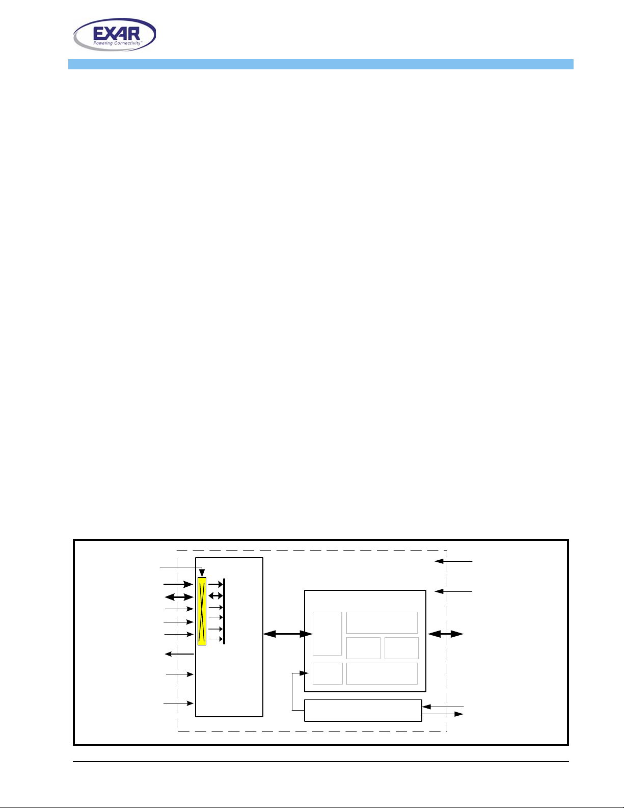
F
IGURE
1. XR16M780 B
PwrSave
A2:A0
D7:D0
IOR#
IOW# (R/W#)
CS#
INT (IRQ# )
RESET
(RESET#)
16/68#
Exar
Corporation 48720 Kato Road, Fremont CA, 94538 • (510) 668-7000 • FAX (510) 668-7017 • www.exar.com
LOCK DIAGRAM
Inte l o r
Motorola
Data Bu s
Inte r fa c e
UART
UART
64 B y te T X F IF O
Regs
BRG
TX &
RX
64 B y te RX F IFO
Cry s ta l Os c /B u ffe r
IR
ENDEC
VCC
(1.62 to 3 .6 3 V )
GND
TX, RX,
RTS#, CTS#,
DTR#, DSR#,
RI#, CD#
XTAL1
XTAL2
Page 2
XR16M780
1.62V TO 3.63V HIGH PERFORMANCE UART WITH 64-BYTE FIFO
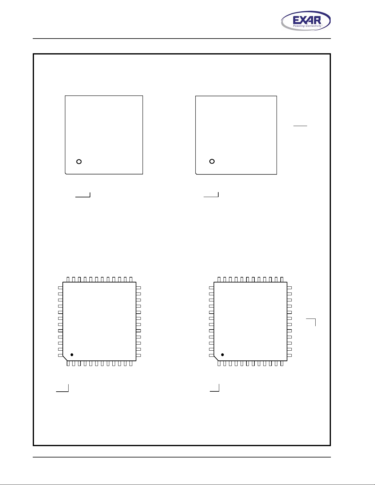
F
IGURE
2. PIN OUT A
CD#
RI#
VCC
D0
D1
D2
D3
25
26
27
28
29
30
31
32
VCC
DSR#
SSIGNMENT FOR
RESET
DTR#
CTS#
24
23
22 21 20 19
32- pin Q F N in
Intel Bus Mode
23456
1
D4
D5
16/68#
RTS#
INT
D6
D7RXTX
32-
A0A1A2
18
17
16
15
14
13
12
11
10
78
CS
PIN
9
QFN
NC
NC
#
IOR
GND
#
IOW
2
XTAL
1
XTAL
PwrSave
AND
48-
DSR#
CD#
RI#
VCC
D0
D1
D2
D3
PIN
TQFP P
25
26
27
28
29
30
31
32
GND
CTS#
23 22 21 20 19 18 17
24
23456
1
D4
ACKAGES IN
RESET#
RTS#
IRQ#
DTR#
A0A1A2
32- p in Q FN in
Moto ro la B u s
Mode
D6
D7RXTX
D5
16/68#
16
78
AND
CS#
68 M
16
15
14
13
12
11
10
9
ODE
NC
NC
IOR#
GND
R/W#
XTAL 2
XTAL 1
PwrSave
REV. 1.0.0
VCC
NC
CTS#
DSR#
CD#
RI#
VCC
D0
D1
D2
D3
D4
NC
VCC
RESETNCDTR#
RTS#NCINTNCA0A1A2NCNC
36 35 34 33 32 31 30 29 28 27 26 25
37
38
39
40
41
42
43
44
45
46
47
48
48-TQFP in
Intel Bus Mode
1 2 3 4 5 6 7 8 9 10 11 1 2
D5D6D7
NC
NC
RX
TX
NC
NC
16/68#
RESET#NCDTR#
NC
36 35 34 33 32 31 30 29 28 27 26 25
24
NC
23
NC
22
NC
21
NC
20
NC
19
IOR#
18
GND
17
NC
16
IOW #
15
XTAL2
14
XTAL1
13
PwrSave
NC
CS#
CTS#
DSR#
CD#
VCC
NC
RI#
D0
D1
D2
D3
D4
NC
37
38
39
40
41
42
43
Motorola Bus Mode
44
45
46
47
48
1 2 3 4 5 6 7 8 9 1 0 1 1 1 2
RTS#NCIRQ#NCA0A1A2
48-TQFP in
D5D6D7
NC
NC
RX
TX
NC
NC
24
23
22
21
20
19
18
17
16
15
14
13
CS#
NC
NC
NC
NC
NC
NC
NC
IOR#
GND
NC
R/W#
XTAL2
XTAL1
PwrSave
VCC
16/68#
GND
2
Page 3
XR16M780
REV. 1.0.0
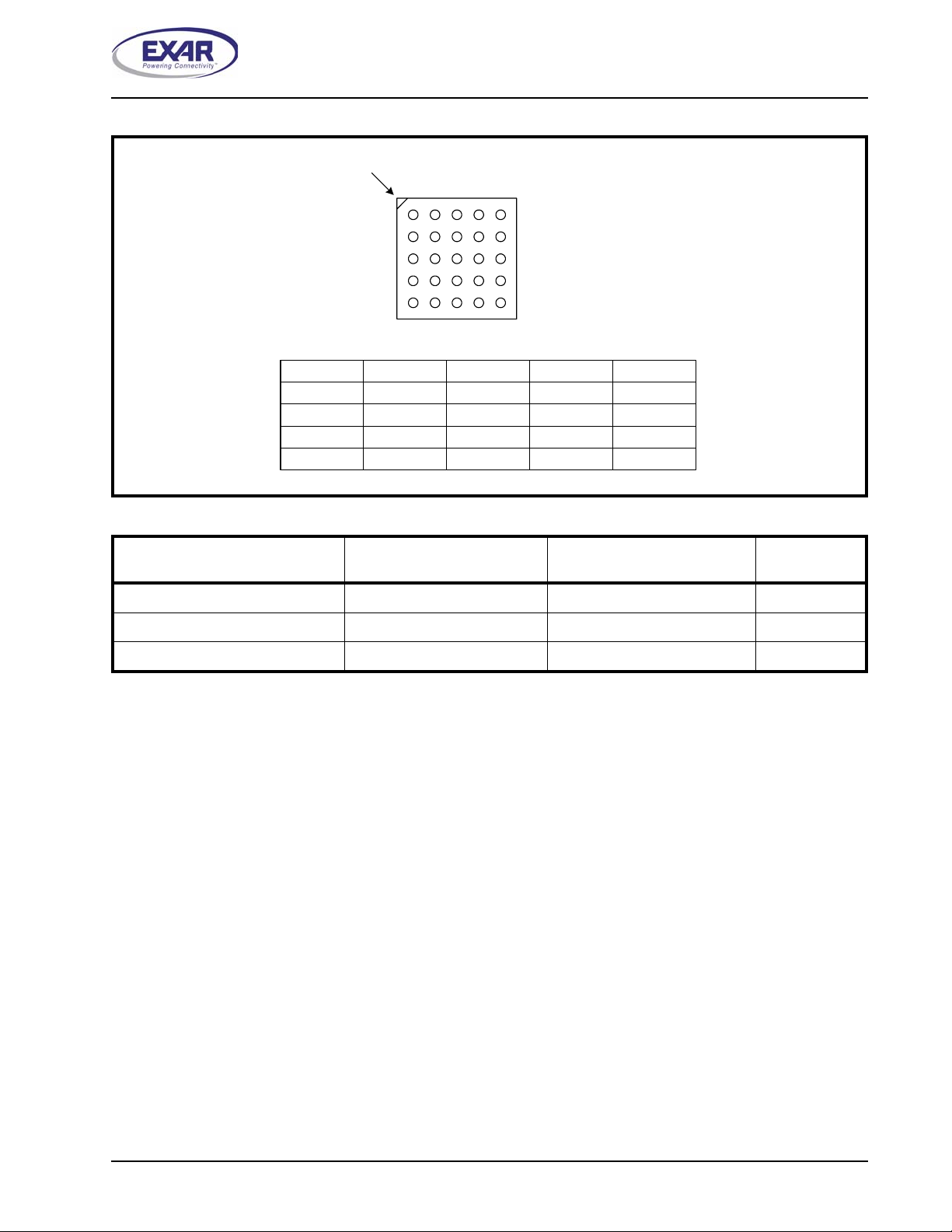
F
IGURE
3. PIN OUT A
SSIGNMENT FOR
ORDERING INFORMATION
1.62V TO 3.63V HIGH PERFORMANCE UART WITH 64-BYTE FIFO
25-
PIN
BGA P
ACKAGE
A1 Corner
1 2 3 4 5
A
B
C
D
E
Transparent Top View
CTS# RESET INT A1 A2
VCC 16/68# RTS# A0 IOR#
D0 D6 D7 PwrSave IOW#
D3 D1 TX CS# XTAL1
D4 D2 D5 RX GND
O
P
ART NUMBER
XR16M780IL32 32-Pin QFN -40°C to +85°C Active
XR16M780IM48 48-Lead TQFP -40°C to +85°C Active
XR16M780IB25 25-Pin BGA -40°C to +85°C Active
P
ACKAGE
PERATING TEMPERATURE
ANGE
R
D
EVICE STATUS
3
Page 4
XR16M780
1.62V TO 3.63V HIGH PERFORMANCE UART WITH 64-BYTE FIFO
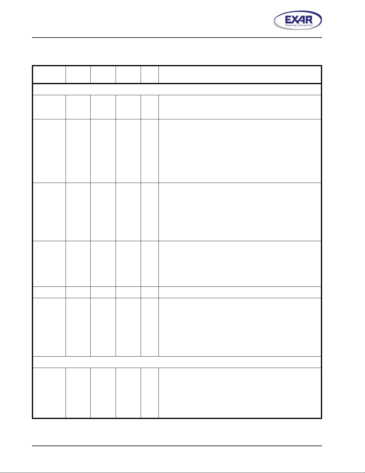
PIN DESCRIPTIONS
Pin Description
N
AME
DA TA BUS INTERFACE
A2
A1
A0
D7
D6
D5
D4
D3
D2
D1
D0
IOR# 14 19 B5 I
IOW#
(R/W#)
CS# 8 11 D4 I
32-QFN
PIN#
48-TQFP
PIN#
17
18
19
5
4
3
1
32
31
30
29
12 16 C5 I
26
27
28
47
46
45
44
43
25-BGA
PIN#
A5
A4
B4
4
3
2
C3
C2
E3
E1
D1
E2
D2
C1
T
YPE
I
Address lines [2:0]. These 3 address lines select the internal registers in UART channel during a data bus transaction.
I/O
Data bus lines [7:0] (bidirectional).
When 16/68# pin is at logic 1, the Intel bus interface is selected and
this input becomes read strobe (active low). The falling edge insti
gates an internal read cycle and retrieves the data byte from an
internal register pointed by the address lines [A2:A0], puts the data
byte on the data bus to allow the host processor to read it on the ris
ing edge.
When 16/68# pin is at logic 0, the Motorola bus interface is selected
and this input should be connected to VCC.
When 16/68# pin is at logic 1, it selects Intel bus interface and this
input becomes write strobe (active low). The falling edge instigates
the internal write cycle and the rising edge transfers the data byte
on the data bus to an internal register pointed by the address lines.
When 16/68# pin is at logic 0, the Motorola bus interface is selected
and this input becomes read (logic 1) and write (logic 0) signal.
This input is chip select (active low) to enable the device.
D
ESCRIPTION
REV. 1.0.0
-
-
INT
(IRQ#)
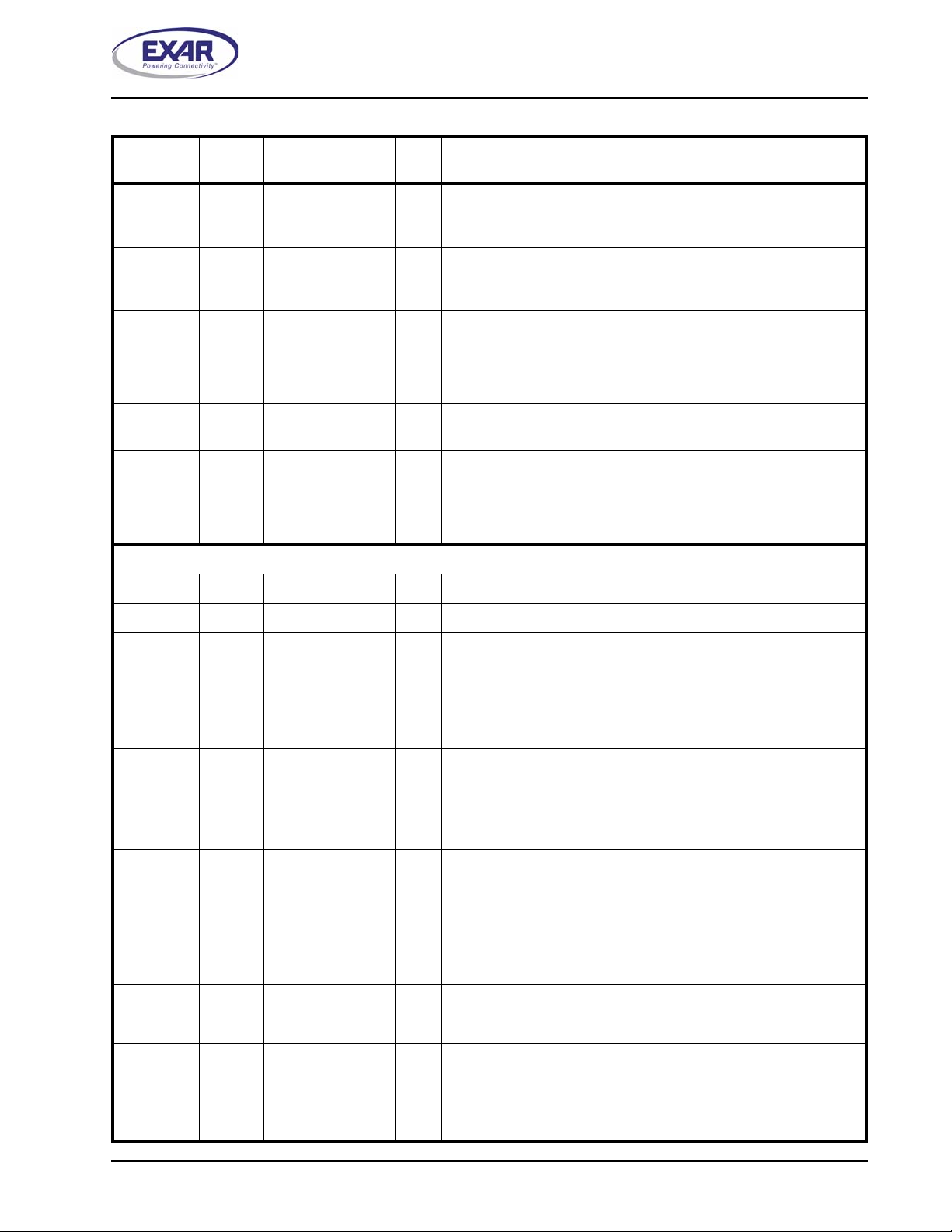
MODEM OR SERIAL I/O INTERFACE
TX 7 8 D3 O
20 30 A3 O
When 16/68# pin is at logic 1 for Intel bus interface, this output
(OD)
become the active high device interrupt output. The output state is
defined by the user through the software setting of MCR[3]. INT is
set to the active mode when MCR[3] is set to a logic 1. INT is set to
the three state mode when MCR[3] is set to a logic 0. See MCR[3].
When 16/68# pin is at logic 0 for Motorola bus interface, this output
becomes the active low device interrupt output (open drain). An
external pull-up resistor is required for proper operation.
UART Transmit Data or infrared encoder data. S tandard transmit
and receive interface is enabled when MCR[6] = 0. In this mode,
the TX signal will be a logic 1 during reset or idle (no data). Infrared
IrDA transmit and receive interface is enabled when MCR[6] = 1. In
the Infrared mode, the inactive state (no data) for the Infrared
encoder/decoder interface is a logic 0. If it is not used, leave it
unconnected.
4
Page 5
XR16M780
REV. 1.0.0
Pin Description
N
AME
RX 6 7 E4 I
RTS# 21 32 B3 O
CTS# 24 38 A1 I
DTR# 22 33 - O
DSR# 25 39 - I
CD# 26 40 - I
RI# 27 41 - I
32-QFN
PIN#
48-TQFP
PIN#
25-BGA
PIN#
1.62V TO 3.63V HIGH PERFORMANCE UART WITH 64-BYTE FIFO
YPE
T
UART Receive Data or infrared receive data. Normal receive data
input must idle at logic 1 condition. The infrared receiver idles at
logic 0. This input should be connected to VCC when not used.
UART Request-to-Send (active low) or general purpose output.
This output must be asserted prior to using auto RTS flow control,
see EFR[6], MCR[1] and IER[6].
UART Clear-to-Send (active low) or general purpose input. It can
be used for auto CTS flow control, see EFR[7], MSR[4] and IER[7].
This input should be connected to VCC when not used.
UART Data-Terminal-Ready (active low) or general purpose output.
UART Data-Set-Ready (active low) or general purpose input. This
input should be connected to VCC when not used.
UART Carrier-Detect (active low) or general purpose input. This
input should be connected to VCC when not used.
UART Ring-Indicator (active low) or general purpose input. This
input should be connected to VCC when not used.
D
ESCRIPTION
ANCILLARY SIGNALS
XTAL1 10 14 D5 I
XTAL2 11 15 - O
PwrSave 9 13 C4 I
16/68# 2 1 B2 I
RESET
(RESET#)
VCC 28 42 B1 Pwr
GND 13 18 E5 Pwr
23 35 A2 I
Crystal or external clock input.
Crystal or buffered clock output.
Power-Save (active high). This feature isolates the M780’s data bus
interface from the host preventing other bus activities that cause
higher power drain during sleep mode. See Sleep Mode with Auto
Wake-up and Power-Save Feature section for details. This pin does
not have an internal pull-down resistor. This input should be con
nected to GND when not used.
Intel or Motorola Bus Select. When 16/68# pin is at logic 1, 16 or
Intel Mode, the device will operate in the Intel bus type of interface.
When 16/68# pin is at logic 0, 68 or Motorola mode, the device will
operate in the Motorola bus type of interface. This pin does not
have an internal pull-up or pull-down resistor.
When 16/68# pin is at logic 1 for Intel bus interface, this input
becomes RESET (active high). When 16/68# pin is at logic 0 for
Motorola bus interface, this input becomes RESET# (active low).
A 40 ns minimum active pulse on this pin will reset the internal registers and all outputs of the UART. The UART transmitter output will
be held at logic 1, the receiver input will be ignored and outputs are
reset during reset period (see UART Reset Conditions).
1.62V to 3.63V power supply.
Power supply common, ground.
-
GND Center
Pad
- - Pwr
The center pad on the backside of the QFN package is metallic and
should be connected to GND on the PCB. The thermal pad size on
the PCB should be the approximate size of this center pad and
should be solder mask defined. The solder mask opening should be
at least 0.0025" inwards from the edge of the PCB thermal pad.
5
Page 6
XR16M780
1.62V TO 3.63V HIGH PERFORMANCE UART WITH 64-BYTE FIFO
Pin Description
N
AME
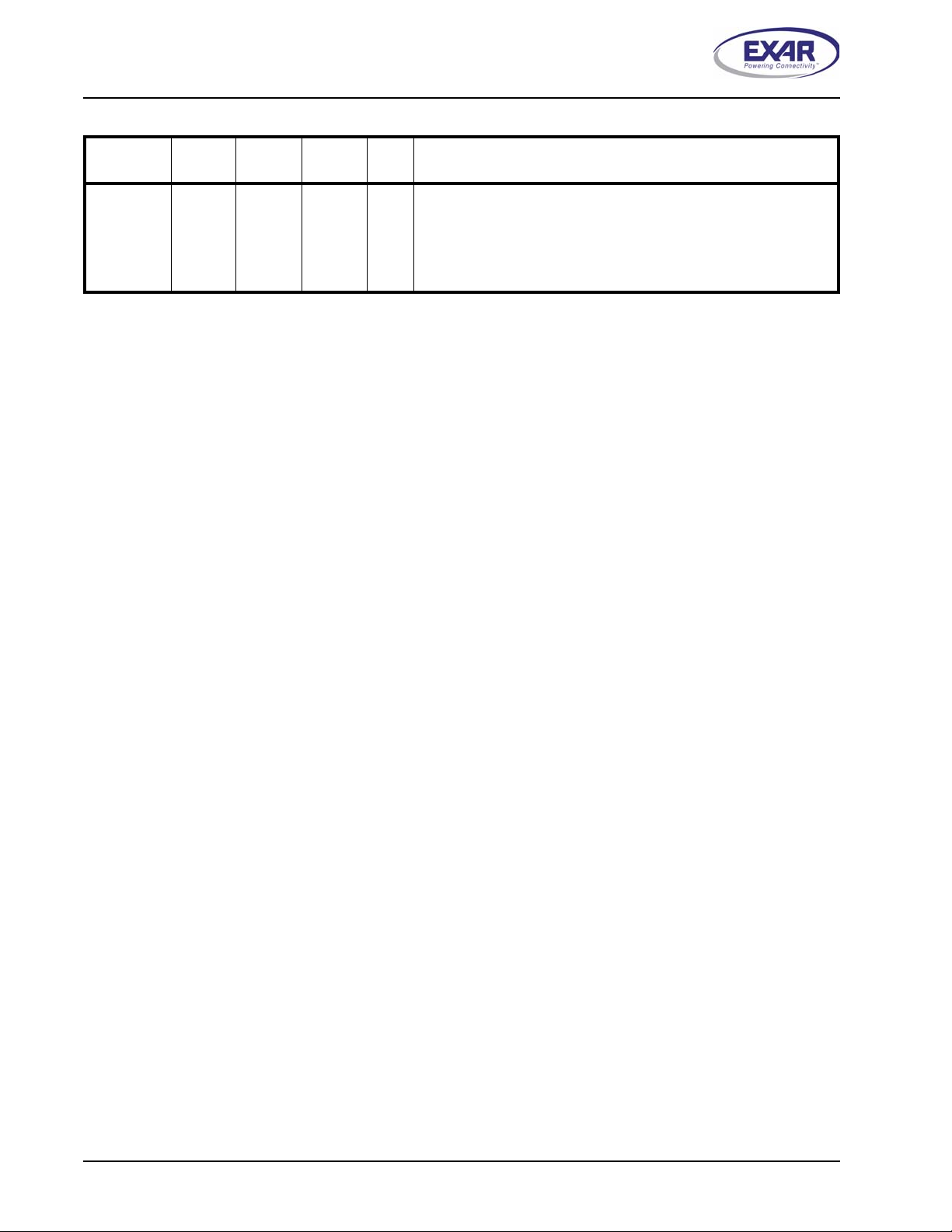
NC 15, 16 5, 6, 9,
Pin type: I=Input, O=Output, I/O= Input/output, OD=Output Open Drain.
32-QFN
PIN#
48-TQFP
PIN#
10, 12,
17, 2025, 29,
31, 34,
36, 37, 48
25-BGA
PIN#
-
T
YPE
-
No Connects.
D
ESCRIPTION
REV. 1.0.0
6
Page 7

XR16M780
REV. 1.0.0
1.0 PRODUCT DESCRIPTION
The XR16M780 (M780) is a high performance single-channel UART. It has its set of device configuration
registers. The configuration registers set is 16550 UART compatible for control, status and data transfer.
Additionally, the M780 channel has 64 bytes of transmit and receive FIFOs, Automatic RTS/CTS Hardware
Flow Control, Automatic Xon/Xoff and Special Character Software Flow Control, infrared en co der an d de cod er
(IrDA ver 1.0 and 1.1), programmable fractional baud rate generator with a prescaler of divide by 1 or 4, and
data rate up to 16 Mbps. The XR16M780 can operate from 1.62 to 3.63 volts. The M780 is fabricated with an
advanced CMOS process.
Larger FIFO
The M780 provides a solution that support s 64 bytes of transmit and receive FIF O memory, instead of 16 bytes
in the XR16L580. The M780 is designed to work with high performance data communication systems, that
requires fast data processing time. Increased performance is realized in the M780 by the larger transmit and
receive FIFOs, FIFO trigger level control and automatic flow control mechanism. This allows the external
processor to handle more networking tasks within a given time. For example, the XR16L580 with a 16 byte
FIFO, unloads 16 bytes of receive data in 1.53 ms (This example uses a character length of 11 bits, including
start/stop bits at 115.2Kbps). This means the external CPU will have to service the receive FIFO at 1.53 ms
intervals. However with the 64 byte FIFO in the M780, the data buffer will not require unloading/loading for 6.1
ms. This increases the service interval giving the external CPU additional time for other applications and
reducing the overall UART interrupt servicing time. In addition, the programmable FIFO level trigger interrupt
and automatic hardware/software flow contr ol is uniq uely pro vided fo r maxim um data throug hput p erforma nce
especially when operating in a multi-channel system. The combination of the above greatly reduces the CPU’s
bandwidth requirement, increases performance, and reduces power consumption.
1.62V TO 3.63V HIGH PERFORMANCE UART WITH 64-BYTE FIFO
Data Rate
The M780 is capable of operation up to 16 Mbps at 3.3V with 4X internal sampling clock rate. The device can
operate at 3.3V with a 24 MHz crystal on pins XTAL1 and XTAL2, or external clock source of 64 MHz on
XTAL1 pin. With a typical crystal of 14 .745 6 M Hz and thro ug h a software option, the user can set t he pr escaler
bit and sampling rate for data rates of up to 3.68 Mbps.
Enhanced Features
The rich feature set of the M780 is available through the internal registers. Automatic hardware/software flow
control, programmable transmit and receive FIFO trigger levels, selectable baud rates, infrared encoder/
decoder, modem interface controls, and a sleep mode are all standard features. MCR bit-5 provides a facility
for turning off (Xon) software flow control with any incoming (RX) character. The M780 includes new features
such as 9-bit (Multidrop) mode, auto RS-485 half-duplex direction control, different baud rate for TX and RX,
fast IR mode and fractional baud rate generator.
7
Page 8
XR16M780
1.62V TO 3.63V HIGH PERFORMANCE UART WITH 64-BYTE FIFO
REV. 1.0.0
2.0 FUNCTIONAL DESCRIPTIONS
2.1 CPU Interface
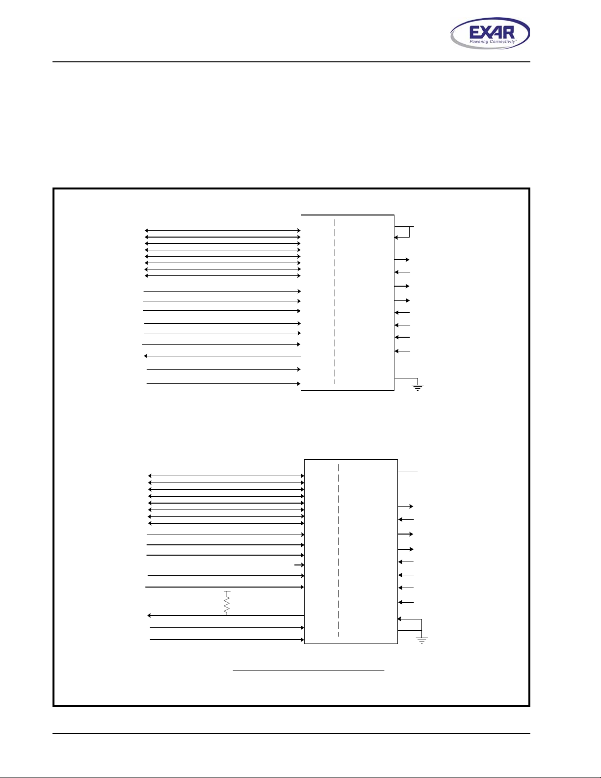
The CPU interface is 8 data bits wide with 3 ad dress lines and control signals to execute data bus read and
write transactions. The M780 data interface supports the Intel and Motorola compatible types of CPUs. No
clock (oscillator nor external clock) is required for a data bus transaction. Each bus cycle is asynchronous
using CS#, IOR# and IOW# or R/W# inputs. A typical data bus interconnection for Intel and Motorola mode is
shown in
F
IGURE
Figure 4.
4. XR16M780 T
IOR#
IOW #
UART_CS#
UART_INT
POWERSAVE
UART_RESET RESET
YPICAL INTEL/MOTOROLA DATA BUS INTERCONNECTIONS
D0
D1
D2
D3
D4
D5
D6
D7
A0
A1
A2
D0
D1
D2
D3
D4
D5
D6
D7
A0
A1
A2
IOR#
IOW#
CS#
INT
PwrSave
16/68#
TX
RX
DTR#
RTS#
CTS#
DSR#
CD#
RI#
GND
VCCVCC
Serial Transceivers of
RS-232
RS-485
RS-422
Or Infrared
Intel Data Bus Interconnections
D0
D1
D2
D3
D4
D5
D6
D7
A0
A1
A2
R/W#
UART_CS#
UART_IRQ#
POWERSAVE
UART_RESET# RESET
vcc
VCC
D0
D1
D2
D3
D4
D5
D6
D7
A0
A1
A2
IOR #
IOW #
CS#
INT
PwrSave
Motorola Data Bus Interconnections
DTR#
RTS#
CTS#
DSR#
CD#
RI#
16/68#
GND
TX
RX
VCCVCC
Serial Transceivers of
RS-232
RS-485
RS-422
Or Infrared
8
Page 9
XR16M780
REV. 1.0.0
1.62V TO 3.63V HIGH PERFORMANCE UART WITH 64-BYTE FIFO
2.2 Serial Interface
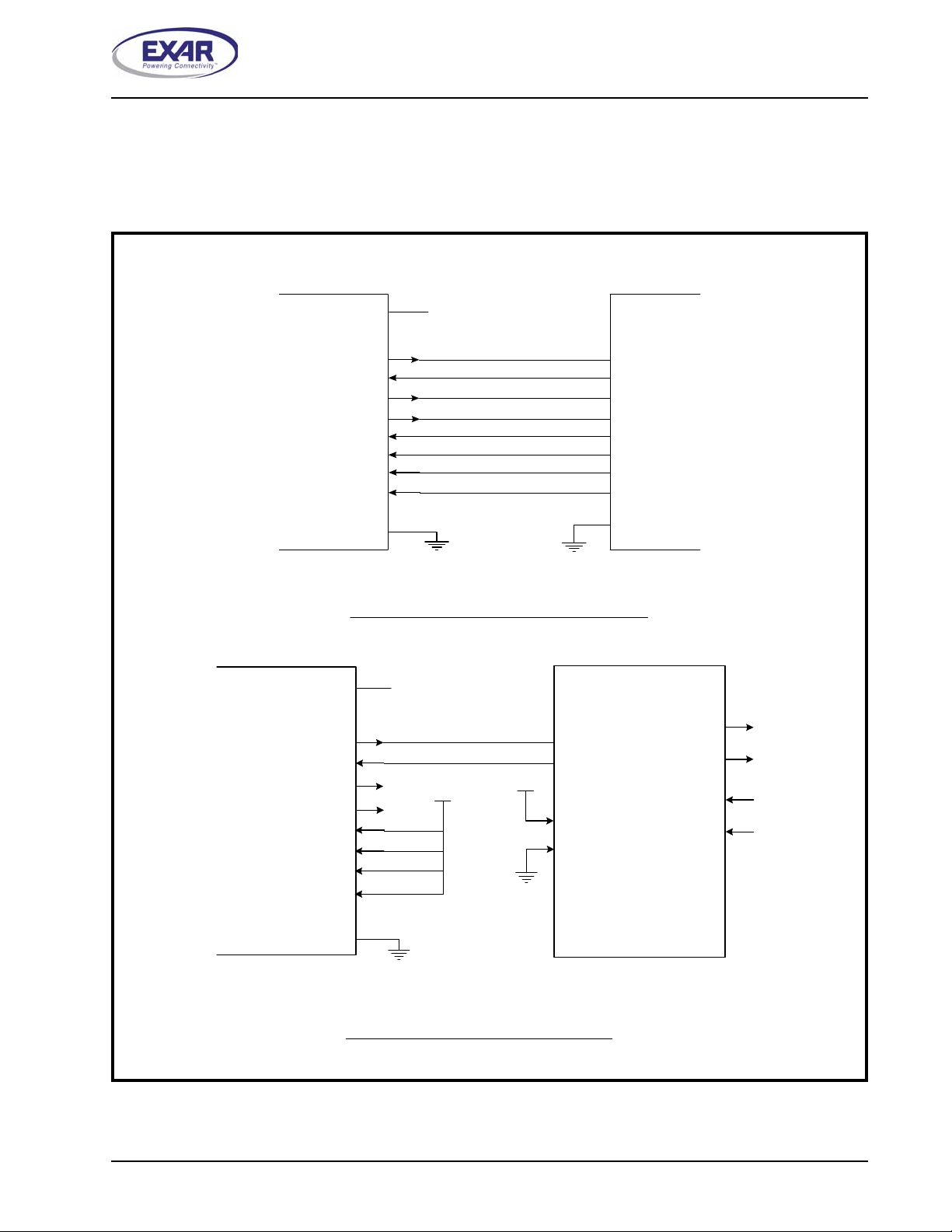
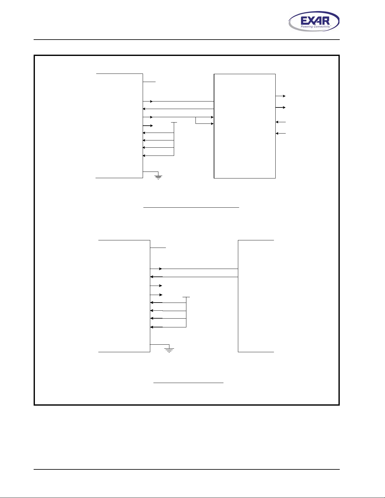
The M780 is typically used with RS-232, RS-485 and IR transceivers. The following figure shows typical
connections from the UART to the different transceivers. For more information on RS-232 and RS-485/422
transceivers, go to www.exar.com or send an e-mail to [email protected].
F
IGURE
5. XR16M780 T
YPICAL SERIAL INTERFACE CONNECTIONS
VCCVCC
TX
RX
DTR#
UART
RTS#
CTS#
DSR#
CD#
RI#
GND
RS -232
Transceiver
T1IN
R1OUT
T2IN
T3IN
R2OUT
R3OUT
R4OUT
R5OUT
GND
UART
R S-23 2 Fu ll -Modem S e r ia l In terfa c e
NC
NC
VCC
DI
RO
VCC
VCC
DE
RE#
VCC
TX
RX
RTS#
DTR#
CTS#
DSR#
CD
RI
GND
#
#
RS-485 Full-Duplex Serial Interface
RS-485
Transceiver
Full-duplex
TX+
TX-
RX+
RX-
9
Page 10
XR16M780
1.62V TO 3.63V HIGH PERFORMANCE UART WITH 64-BYTE FIFO
F
IGURE
6. XR16M780 T
YPICAL SERIAL INTERFACE CONNECTIONS
UART
VCC
RTS#
DTR#
CTS#
DSR#
CD
RI
GND
TX
RX
#
#
NC
VCC
VCC
RS-485 Half-Duplex Serial Interface
DI
RO
DE
RE#
RS-485
Transceiver
Half-duplex
REV. 1.0.0
Y
Z
A
B
UART
TX
RX
DTR#
RTS#
CTS#
DSR#
CD#
RI#
GND
VCCVCC
NC
NC
VCC
Infrared Connection
IR
Transceiver
TXD
RXD
10
Page 11
XR16M780
REV. 1.0.0
1.62V TO 3.63V HIGH PERFORMANCE UART WITH 64-BYTE FIFO
2.3 Device Reset
The RESET input resets the internal registers and the serial interface outputs to their default state (see
Table 18). An active high pulse of longer than 40 ns duration will be required to ac tivate the reset function in
the device. Following a power-on reset or an exte rnal reset, the M780 is software compatible with previous
generation of UARTs, XR16L580 and ST16C550.
2.4 Internal Registers
The M780 has a set of 16550 compatible registers for controlling, monitoring and data loading and unloading.
These registers function as data holding registers (THR/RHR), interrupt status and control registers (ISR/IER),
a FIFO control register (FCR), receive line status and control registers (LSR/LCR), modem status and control
registers (MSR/MCR), programmable dat a rate (clo ck) divisor registe rs (DLL/DLM/DLD), an d a user accessibl e
scratchpad register (SPR).
Beyond the general 16C550 features an d cap abiliti es, the M780 offers enhanced feature regist ers (EFR, Xon 1/
Xoff 1, Xon2/Xoff 2, DLD, FCTR, EMSR, FC and TRIG) that provide automatic RTS and CTS hardware flow
control, automatic Xon/Xoff software flow control, 9-bit (Multidrop) mode, auto RS-485 half duplex control,
different baud rate for TX and RX an d fr act iona l bau d rate gene ra to r. All the register functions are discussed in
full detail later in
“Section 3.0, UART INTERNAL REGISTERS” on page 25.
2.5 INT Ouput
The interrupt outputs change according to the operating mode and enhanced features setup. Table 1 and 2
summarize the operating behavior for the transmitter and receiver. Also see Figure 22 through 25.
N
OTE
: The IRQ# pin requires a pull-up resistor for proper operation.
INT Pin
(16/68# = 1)
IRQ# Pin
(16/68# = 0)
INT Pin
(16/68# = 1)
IRQ# Pin
(16/68# = 0)
T
ABLE
1: INT PIN O
FCR BIT-0 = 0 (FIFO D
LOW = One byte in THR
HIGH = THR empty
HIGH = One byte in THR
LOW = THR empty
T
ABLE
FCR BIT-0 = 0 (FIFO D
HIGH = One byte in RHR
LOW = RHR empty
LOW = One byte in RHR
HIGH = RHR empty
PERATION FOR TRANSMITTER
ISABLED
) FCR BIT-0 = 1 (FIFO E
2: INT PIN O
ISABLED
) FCR BIT-0 = 1 (FIFO E
NABLED
LOW = FIFO above trigger level
HIGH = FIFO below trigger level or FIFO empty
HIGH = FIFO above trigger level
LOW = FIFO below trigger level or FIFO empty
PERATION FOR RECEIVER
NABLED
LOW = FIFO below trigger level
HIGH = FIFO above trigger level or RX Data Timeout
HIGH = FIFO below trigger level
LOW = FIFO above trigger level or RX Data Timeout
)
)
11
Page 12
XR16M780
1.62V TO 3.63V HIGH PERFORMANCE UART WITH 64-BYTE FIFO
REV. 1.0.0
2.6 Crystal Oscillator or External Clock Input
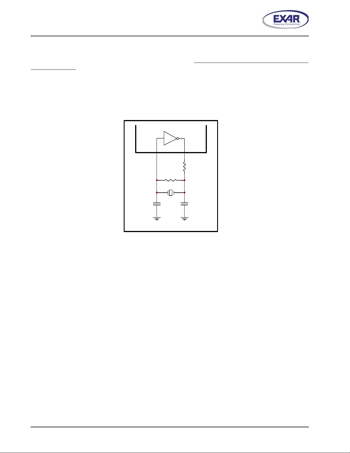
The M780 includes an on-chip oscillator to produce a clock for the baud rate generators in the device when a
crystal is connected between XTAL1 and XTAL2 as show below.
The CPU data bus does not require this clock
for bus operation. The crystal oscillator provides a system clock to the Baud Rate Generators (BRGs) in the
UART. XTAL1 is the input to the oscillator or external clock buffer input with XTAL2 pin being the output. For
programming details, see
“Section 2.7, Programmable Baud Rate G enerator with Fractional Divisor” on
page 13.
F
IGURE
7. T
YPICAL CRYSTAL CONNECTIONS
XTAL1 XTAL2
R2
500K - 1M
C1
22-47pF
22-47pF
Y1
C2
R1
0-120
(O p tional)
1.8432 MHz
to
24 MHz
The on-chip oscillator is designed to use an industry standard microprocessor crystal (parallel resonant,
fundamental frequency with 10-22 pF capacitance load, ESR of 20-120 ohms and 100ppm frequency
tolerance) connected externally between the XTAL1 and XTAL2 pins. Typical oscillator connections are shown
in
Figure 7. Alternatively, an external clock can be connected to the XTAL1 pin to clock the internal baud rate
generator for standard or custom rates. The BGA package has XTAL1 only, the external clock is required. For
further reading on oscillator circuit, see application note DAN108 on EXAR’s web site.
12
Page 13
XR16M780
REV. 1.0.0
1.62V TO 3.63V HIGH PERFORMANCE UART WITH 64-BYTE FIFO
2.7 Programmable Baud Rate Generator with Fractional Divisor
The M780 has independent Baud Rate Generators (BRGs) with prescalers for the transmitter and receiver.
The prescalers are controlled by a software bit in the MCR register. The MCR register bit-7 sets the prescalers
to divide the input crystal or external clock by 1 or 4. The output of the prescaler clocks to the BRG. The BRG
further divides this clock by a programmable divisor between 1 and (2
16
- 0.0625) in increments of 0.0625 (1/
16) to obtain a 16X or 8X or 4X sampling clock of the serial data rate. The sampling clock is used by the
transmitter for data bit shifting and receiver for data sampling. For transmitter and receiver, the M780 provides
respective BRG divisors. The BRG divisor (DLL, DLM, and DLD registers) defaults to the value of ’1’ (DLL =
0x01, DLM = 0x00 and DLD = 0x00) upo n rese t. Th er ef or e, th e BRG mu st be pr og ra m me d durin g in itia liza tion
to the operating data rate. The DLL and DLM registers provide the integer part of the divisor and the DLD
registers provides the fractional part of the divisor. The four lower bits of the DLD are used to select a value
from 0 (for setting 0000) to 0.9375 or 15/16 (for setting 1111). Programming the Baud Rate Generator
Registers DLL, DLM and DLD provides the capability for selecting the operating data rate.
Table 3 shows the
standard data rates available with a 24MHz crystal or external clock at 16X clock rate. If the pre-scaler is used
(MCR bit-7 = 1), the output data rate will be 4 times less than t hat shown in
Table 3. At 8X sampling rate, these
data rates would double. And at 4X sampling rate, they would quadruple. Also, when using 8X sampling mode,
please note that the bit-time will have a jitter (+/- 1/ 16) whenever the DLD is non-ze ro and is an odd number.
When using a non-standard data rate crystal or external clock, the divisor value can be calculated with the
following equation(s):
Required Divisor (decimal)=(XTAL1 clock frequency / prescaler) /(serial data rate x 16), with 16X mode,
DLD[5:4]=’00’
Required Divisor (decimal)= (XTAL1 clock frequency / prescaler / (serial data rate x 8), with 8X mode,
Required Divisor (decimal)= (XTAL1 clock frequency / prescaler / (serial data rate x 4), with 4X mode,
DLD[5:4] = ’01’
DLD[5:4] = ’10’
The closest divisor that is obtainable in the M780 can be calculated using the following formula:
ROUND( (Required Divisor - TRUNC(Required Divisor) )*16)/16 + TRUNC(Required Divisor), where
DLM = TRUNC(Required Divisor) >> 8
DLL = TRUNC(Required Divisor) & 0xFF
DLD = ROUND( (Required Divisor-TRUNC(Required Divisor) )*16)
In the formulas above, please note that:
TRUNC (N) = Integer Part of N. For example, TRUNC (5.6) = 5.
ROUND (N) = N rounded towards the closest integer. For example, ROUND (7.3) = 7 and ROUND (9.9) = 10.
A >> B indicates right shifting the value ’A’ by ’B’ number of bits. For example, 0x78A3 >> 8 = 0x0078.
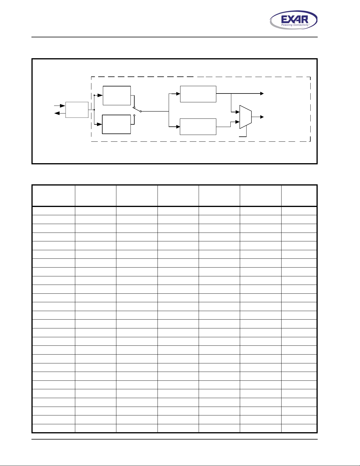
2.7.1 Independent TX/RX BRG
The XR16M780 has two independent sets of TX and RX baud rate generator. See Figure 8. TX and RX can
work in different baud rate by setting DLD, DLL and DLM register. For example, TX can transmit data to the
remote UART at 9600 bp s while RX r eceives data from remote UAR T at 921. 6 Kbps. For the baud rate set ting,
please
See ”Section 4.13, Baud Rate Generator Registers (DLL, DLM and DLD) - Read/Write” on
page 39.
13
Page 14
XR16M780
1.62V TO 3.63V HIGH PERFORMANCE UART WITH 64-BYTE FIFO
F
IGURE
8. B
AUD RATE GENERATOR
XTAL1
XTAL2
T
ABLE
Required
Output Data
Rate
Prescaler
Divide by 1
Crystal
Osc
/
Buffer
Prescaler
Divide by 4
3: T
YPICAL DATA RATES WITH A
D
IVISOR FOR
Clock
16x
O
(Decimal)
MCR Bit 7=0
(default)
MCR Bit-7=1
D
IVISOR
BTAINABLE IN
M780
DLD[7]=0
-
DLD[7]=1
24 MHZ
DLM P
ALUE
V
CRYSTAL OR EXTERNAL CLOCK AT
ROGRAM
(HEX)
DLL
DLM
DLD[5:0]
DLL
DLM
DLD[5:0]
DLL P
ALUE
V
DLD[6]
ROGRAM
(HEX)
0
1
DLD P
ALUE
V
400 3750 3750 E A6 0 0
2400 625 625 2 71 0 0
4800 312.5 312 8/16 1 38 8 0
9600 156.25 156 4/16 0 9C 4 0
10000 150 150 0 96 0 0
19200 78.125 78 2/16 0 4E 2 0
25000 60 60 0 3C 0 0
28800 52.0833 52 1/16 0 34 1 0.04
38400 39.0625 39 1/16 0 27 1 0
50000 30 30 0 1E 0 0
57600 26.0417 26 1/16 0 1A 1 0.08
75000 20 20 0 14 0 0
100000 15 15 0 F 0 0
115200 13.0208 13 0 D 0 0.16
153600 9.7656 9 12/16 0 9 C 0.16
200000 7.5 7 8/16 0 7 8 0
225000 6.6667 6 11/16 0 6 B 0.31
230400 6.5104 6 8/16 0 6 8 0.16
250000 6 6 0 6 0 0
300000 5 5 0 5 0 0
400000 3.75 3 12/16 0 3 C 0
460800 3.2552 3 4/16 0 3 4 0.16
500000 3 3 0 3 0 0
750000 2 2 0 2 0 0
921600 1.6276 1 10/16 0 1 A 0.16
1000000 1.5 1 8/16 0 1 8 0
16X or 8X or 4X
Sampling Rate Clock
16X or 8X or 4X
Sampling Rate Clock
16X S
ROGRAM
(HEX)
REV. 1.0.0
to Transmitter
to Receiver
AMPLING
D
ATA ERROR
ATE
R
(%)
14
Page 15
XR16M780
REV. 1.0.0
1.62V TO 3.63V HIGH PERFORMANCE UART WITH 64-BYTE FIFO
2.8 Transmitter
The transmitter section comprises of an 8-bit Transmit Shift Register (TSR) and 64 bytes of FIFO which
includes a byte-wide Transmit Holding Register (THR). TSR shifts out every data bit with the 16X/8X/4X
internal clock. A bit time is 16/8/4 clock periods. The transmitter sends the start-bit followed by the number of
data bits, inserts the proper parity-bit if enabled, and adds the stop-bit(s). The status of the FIFO and TSR are
reported in the Line Status Register (LSR bit-5 and bit-6).
2.8.1 Transmit Holding Register (THR) - Write Only
The transmit holding register is an 8-bit register providing a data interface to the host processor. The host
writes transmit data byte to the THR to be converted into a serial data stream including start-bit, data bits,
parity-bit and stop-bit(s). The least-significant-bit (Bit-0) becomes first data bit to go out. The THR is the input
register to the transmit FIFO of 64 bytes when FIFO operation is enabled by FCR bit-0. Every time a write
operation is made to the THR, the FIFO data pointer is automatically bumped to the next sequential data
location.
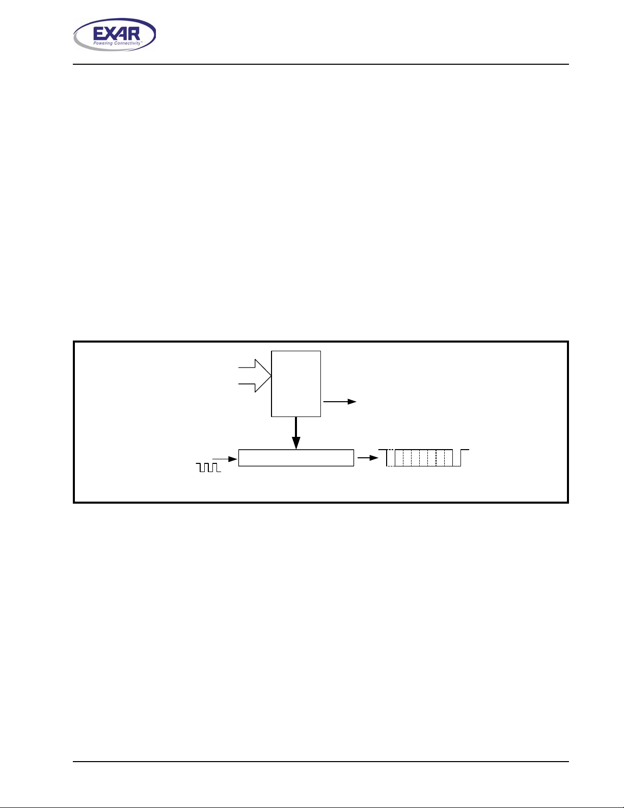
2.8.2 Transmitter Operation in non-FIFO Mode
The host loads transmit data to THR one character at a time. The THR empty flag (LSR bit-5) is set when the
data byte is transferred to TSR. THR fla g can gener ate a tr ansmit emp ty interru pt (ISR bit-1 ) when it is enable d
by IER bit-1. The TSR flag (LSR bit-6) is set when TSR becomes completely empty.
F
IGURE
9. T
RANSMITTER OPERATION IN NON
-FIFO M
ODE
Data
Byte
16X or 8X or 4X
Clock
( DLD[5:4] )
Transmit
Holding
Register
(THR)
Transmit Shift Register (TSR)
THR Interrupt (ISR bit-1)
Enabled by IER bit-1
M
S
B
L
S
B
TXNOFIFO1
15
Page 16
XR16M780
1.62V TO 3.63V HIGH PERFORMANCE UART WITH 64-BYTE FIFO
REV. 1.0.0
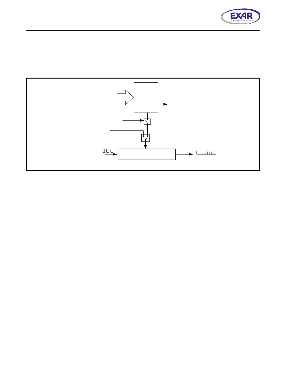
2.8.3 Transmitter Operation in FIFO Mode
The host may fill the transmit FIFO with up to 64 bytes of transmit data. The THR empty flag (LSR bit-5) is set
whenever the FIFO is empty. The THR empty flag can generate a transmit empty interrupt (ISR bit-1) when the
FIFO becomes empty. The transmit empty interrupt is enabled by IER bit-1. The TSR flag (LSR bit-6) is set
when TSR/FIFO becomes empty.
F
IGURE
10. T
RANSMITTER OPERATION IN
Auto CTS Flow Control (CTS# pin)
Flow Control Characters
(Xoff1/2 and Xon1/2 Reg.)
Auto Softw are F low Contr ol
16X or 8X or 4X Clock
(DLD[5 :4 ])
FIFO
Transmit
Data Byte
AND FLOW CONTROL MODE
Transmit
FIFO
Transmit Data Shift Register
(TSR)
THR Inte rr u p t (ISR b it-1 ) fa lls
below the programmed Trigger
Level and then when becomes
empty. FIFO is Enabled by FCR
bit-0=1
TXFIFO1
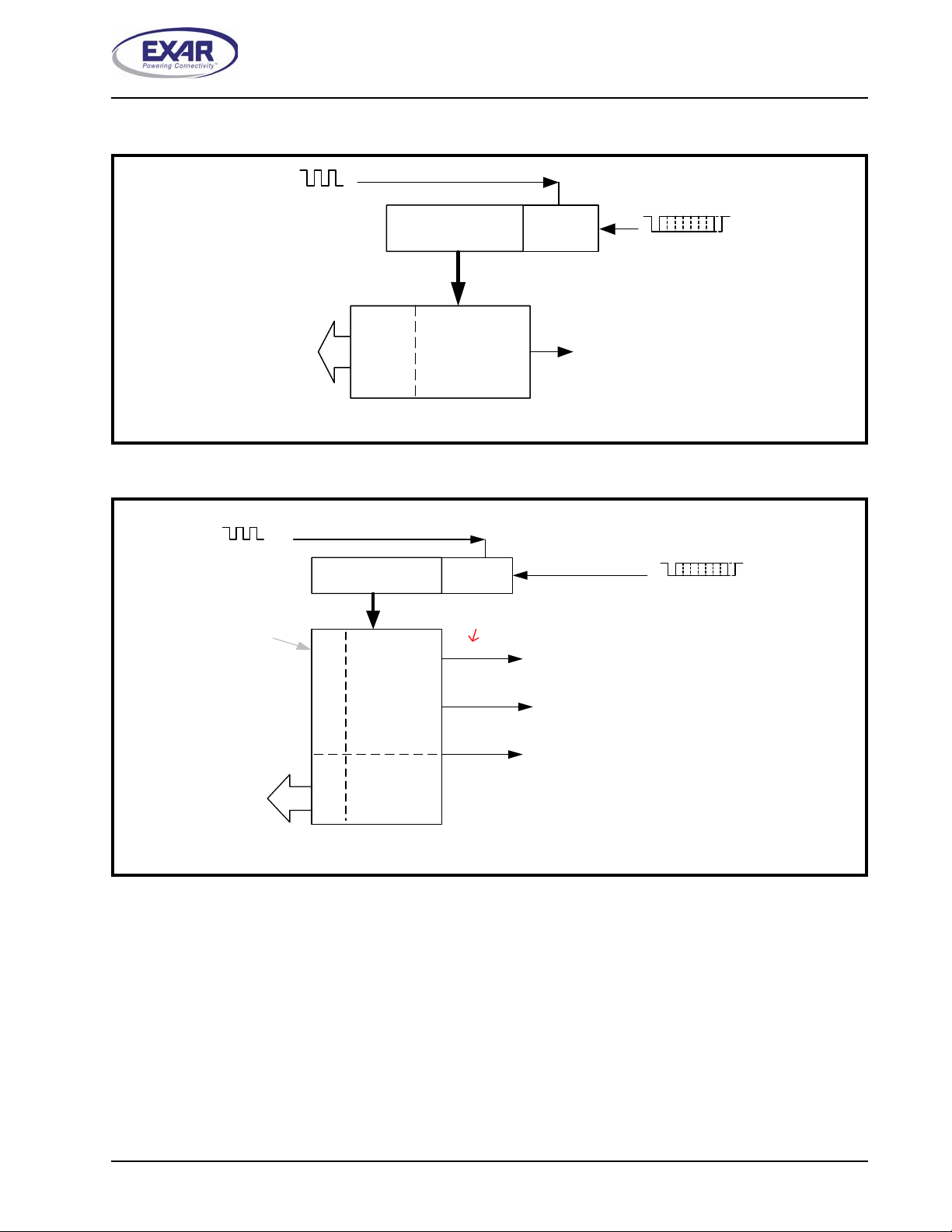
2.9 Receiver
The receiver section contains an 8-bit Receive Shift Register (RSR) and 64 bytes of FIFO which includes a
byte-wide Receive Holding Register (RHR). The RSR uses the 16X/8X/4X clock (DLD[5:4]) for timing. It
verifies and validates every bit on the incoming character in the middle of each data bit. On the falling edge of
a start or false start bit, an internal receiver counter starts counting at th e 16X/8X/4X clock rate. After 8 clocks
(or 4 if 8X or 2 if 4X) the start bit period should be at the center of the start bit. At this time the start bit is
sampled and if it is still a logic 0 it is validated. Evaluating the start bit in this manner prevents the receiver from
assembling a false character. The rest of the data bits and stop bits are sampled and validated in this same
manner to prevent false framing. If t here we re any er ror( s), they a re repor ted in th e LSR register bit s 2- 4. Upon
unloading the receive data byte from RHR, the receive FIFO pointer is bumped and the error tags are
immediately updated to reflect the status of the data byte in RHR register. RHR can generate a receive data
ready interrupt upon receiving a character or delay until it reaches the FIFO trigger level. Furthermore, data
delivery to the host is guaranteed by a receive data ready time-out interrupt when data is not received for 4
word lengths as defined by LCR[1:0] plus 12 bits time. This is equivalent to 3.7-4.6 character times. The RHR
interrupt is enabled by IER bit-0. See
Figure 11 and Figure 12 below.
2.9.1 Receive Holding Register (RHR) - Read-Only
The Receive Holding Register is an 8-bit register that holds a receive data byte from the Receive Shift
Register. It provides the receive data interface to the host processor. The RHR register is part of the receive
FIFO of 64 bytes by 11-bits wide, the 3 extra bits are for the 3 error tags to be reported in LSR re gister. When
the FIFO is enabled by FCR bit-0, the RHR contains the first data character received by the FIFO. After the
RHR is read, the next character byte is loaded into the RHR and the errors associated with the current data
byte are immediately updated in the LSR bits 2-4.
16
Page 17
XR16M780
REV. 1.0.0
F
IGURE
F
IGURE
11. R
ECEIVER OPERATION IN NON
16X or 8X or 4X Clock
( DLD[5:4] )
Receive
Data By te
and Errors
12. R
ECEIVER OPERATION IN
1.62V TO 3.63V HIGH PERFORMANCE UART WITH 64-BYTE FIFO
-FIFO M
Error
Tags in
LSR bits
4:2
FIFO
ODE
Receive Data Shift
Register (RSR)
Receive Data
Holding Register
(RHR)
AND AUTO
RTS F
Data Bit
Validation
Receive Data Characters
RHR Inte rrup t (IS R b it-2)
LOW CONTROL MODE
RXFIFO1
16X or 8X or 4X Clock
( DLD[5:4] )
64 bytes by 11-bit wide
Receive Data
By te a n d Er ro r s
FIFO
Receive Data Shift
Register (RSR)
Receive
Da ta F IF O
(64-sets)
Error Tags
Receive
Data
LSR bits 4:2
Error Tags in
Da ta Bit
Va lidat io n
Example
- RX FIFO trigger level sele cted at 16 bytes
:
Da ta fa l ls to
8
FIFO
Trigger=16
Data fills to
56
(See Note Below)
RTS# re - a s serts wh e n data falls b e lo w th e flo w
con tr o l trig ger le v e l to r e s ta rt r e mo te tr a n s mitte r .
Enable by EFR bit-6=1, MCR bit-1.
RHR Interrupt (ISR bit-2) programmed for
desired FIFO trigger level.
FIFO is Enabled by FCR bit-0=1
RTS# de-asserts when data fills above the flow
control trigger level to suspend remote transmitter.
Enable by EFR bit-6=1, MCR bit-1.
Receive Data Characters
RXFIFO1
17
Page 18
XR16M780
1.62V TO 3.63V HIGH PERFORMANCE UART WITH 64-BYTE FIFO
REV. 1.0.0
2.10 Auto RTS (Hardware) Flow Control
Automatic RTS hardware flow control is used to prevent data overrun to the local receiver FIFO. The RTS#
output is used to request remote unit to suspend/resume data transmission. The auto RTS flow control
features is enabled to fit specific applicatio n req uir em e nt (see
•
Enable auto RTS flow control using EFR bit-6.
•
The auto RTS function must be started by assert ing RTS# outpu t pin (MCR bit-1 to logic 1 af ter it is enabled).
Figure 13):
If using the Auto RTS interrupt:
•
Enable RTS interrupt through IER bit-6 (after setting EFR bit-4). The UART issues an interrupt when the
RTS# pin makes a transition from low to high: ISR bit-5 will be set to logic 1.
2.11 Auto RTS Hysteresis
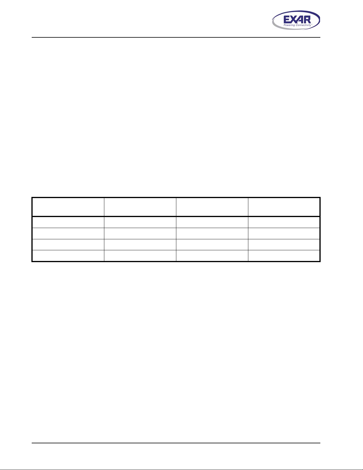
With the Auto RTS function enabled, an interr upt is gener ated when the receive FIFO rea ches the select ed RX
trigger level. The RTS# pin will not be forced HIGH (RTS off) until the receive FIFO reaches one trigger level
above the selected trigger level in the trigger table (
Table 9). The RTS# pin will return LOW after the RX FIFO
is unloaded to one level below the selected trigger level. Under the above described conditions, the M780 will
continue to accept data until the receive FIFO gets full. The Auto RTS function is initiated when the RTS#
output pin is asserted LOW (RTS On).
T
ABLE
4: A
UTO
RX T
RIGGER LEVEL
INT PIN A
RTS (H
CTIVATION
ARDWARE
) F
LOW CONTROL
RTS# DE-
(C
HARACTERS IN RX FIFO
ASSERTED
(H
IGH
)
RTS# A
)
(C
SSERTED
HARACTERS IN RX FIFO
(LOW)
)
8 8 16 0
16 16 56 8
56 56 60 16
60 60 60 56
2.12 Auto CTS Flow Control
Automatic CTS flow control is used to prevent data overrun to the rem ote receiver FIFO. The CTS# input is
monitored to suspend/restart the local transmitter. The auto CTS flow control feature is selected to fit specific
application requirement (see
•
Enable auto CTS flow control using EFR bit-7.
Figure 13):
If needed, the CTS interrupt can be enabled through IER bit-7 (after setting EFR bit-4). The UART issues an
interrupt when the CTS# pin is de-asserted (HIGH): ISR bit-5 will be set to 1, and UART will suspend
18
Page 19
XR16M780
REV. 1.0.0
1.62V TO 3.63V HIGH PERFORMANCE UART WITH 64-BYTE FIFO
transmission as soon as the stop bit of the character in process is shifted out. Transmission is resumed after
the CTS# input is re-asserted (LOW), indicating more data may be sent.
F
IGURE
13. A
UTO
RTS
AND
Local UART
UARTA
Receiver FIFO
Trigger Reached
Auto RTS
Trigger Level
Transmitter
Auto CTS
Monitor
RTSA#
CTSB#
TXB
RXA FIFO
INTA
(RXA FIFO
Interrupt)
CTS F
Data Starts
Receive
Data
LOW CONTROL OPERATION
RXA TXB
RTSA# CTSB#
Assert RTS# to Begin
Transmission
1
ON
2
ON
3
4
RX FIFO
Trigger Level
5
7
8
6
RTS High
Threshold
OFF
OFF
Suspend
RXBTXA
RTSB#CTSA#
Restart
9
RTS Low
Threshold
Remote UART
Trigger Reached
10
ON
11
UARTB
Transmitter
Auto CTS
Monitor
Receiver FIFO
Auto RTS
Trigger Level
ON
RX FIFO
12
Trigger Level
RTSCTS1
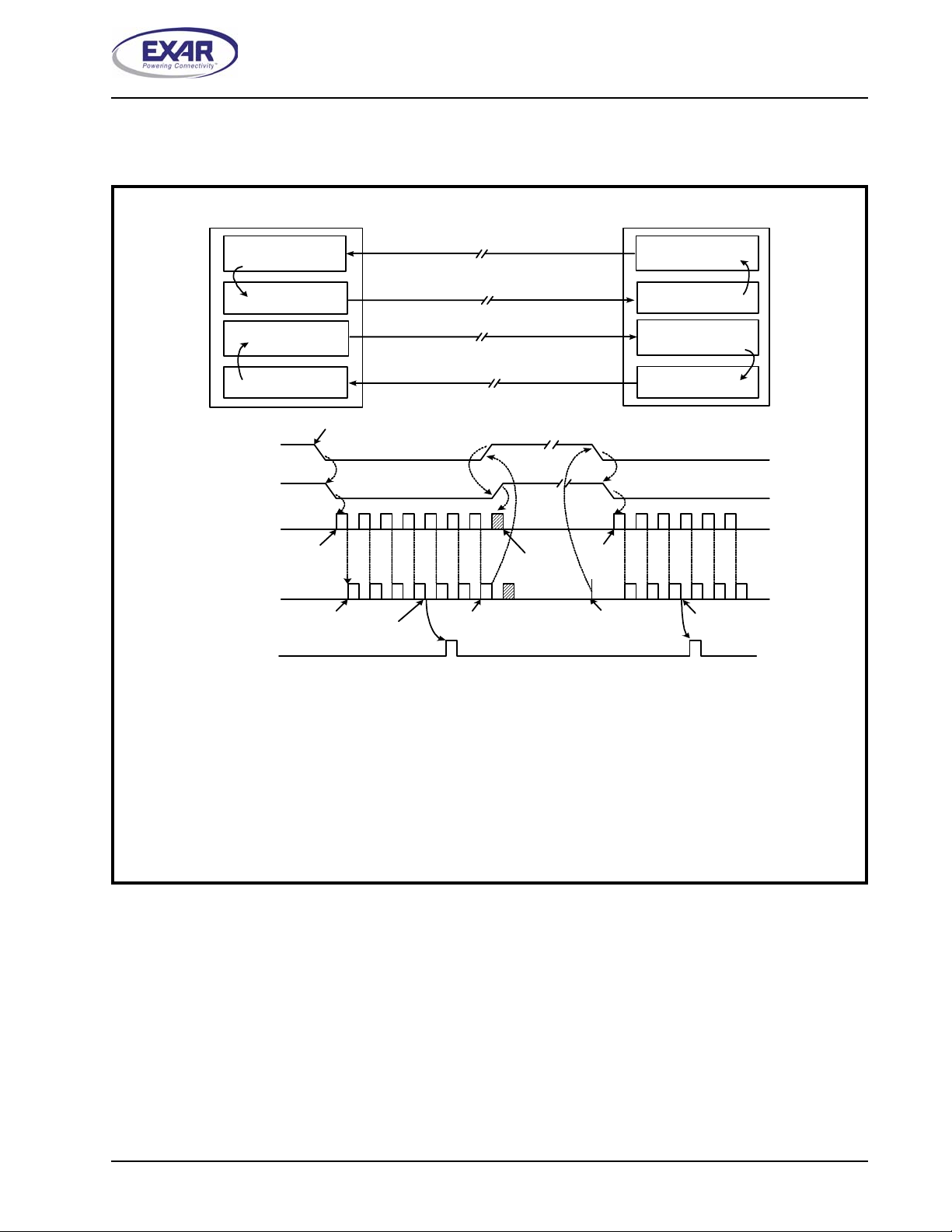
The local UART (UARTA) starts data transfer by asserting RTSA# (1). RTSA# is normally connected to CTSB# (2) of
remote UART (UARTB). CTSB# allows its transmitter to send data (3). TXB data arrives and fills UARTA receive FIFO
(4). When RXA data fills up to its receive FIFO trigger level, UARTA activates its RXA data ready interrupt (5) and continues to receive and put data into its FIFO. If interrupt service latency is long and data is not being unloaded, UARTA
monitors its receive data fill level to match the upper threshold of RTS delay and de-assert RTSA# (6). CTSB# follows
(7) and request UARTB transmitter to suspend data transfer. UARTB stops or finishes sending the data bits in its trans
mit shift register (8). When receive FIFO data in UARTA is unloaded to match the lower threshold of RTS delay (9),
UARTA re-asserts RTSA# (10), CTSB# recognizes the change (11) and restarts its transmitter and data flow again until
next receive FIFO trigger (12). This same event applies to the reverse direction when UARTA sends data to UARTB
with RTSB# and CTSA# controlling the data flow.
-
19
Page 20
XR16M780
1.62V TO 3.63V HIGH PERFORMANCE UART WITH 64-BYTE FIFO
REV. 1.0.0
2.13 Auto Xon/Xoff (Software) Flow Control
When software flow control is enabled (See Table 17), the M780 compares one or two sequential receive data
characters with the programmed Xon or Xoff-1,2 character value(s). If receive character(s) (RX) match the
programmed values, the M780 will halt tran smission (TX) as soon as the current character has completed
transmission. When a match occurs, the Xoff (if enabled via IER bit-5) flag will be set and the interrupt output
pin will be activated. Following a suspension due to a match of the Xoff character, the M780 will monitor the
receive data stream for a match to the Xon-1,2 character. If a match is found, the M780 will resume operation
and clear the flags (ISR bit-4).
Reset initially sets the contents of the Xon/Xoff 8-bit flow control registers to a logic 0. Following reset the user
can write any Xon/Xoff value desired for software flow control. Different conditions can be set to detect Xon/
Xoff characters (
See Table 17) and suspend/resume transmissions. When double 8-bit Xon/Xoff characters
are selected, the M780 compares two consecutive receive characters with two software flow control 8-bit
values (Xon1, Xon2, Xoff1, Xoff2) and controls TX transmissions accordingly. Under the above described flow
control mechanisms, flow control characters are not placed (stacked) in the user accessible RX data buffer or
FIFO.
In the event that the receive buffer is overfilling and flow control needs to be executed, the M780 automatically
sends an Xoff message (when enabled) via the serial TX output to the remote modem. The M780 sends the
Xoff-1,2 characters two-character- times (= time taken to send two characte rs at the programmed baud rate )
after the receive FIFO crosses the programmed trigger level. To clear this condition, the M780 will transmit the
programmed Xon-1,2 characters as soon as receive FIFO is less t ha n on e trigg er level be low th e pr ogra mme d
trigger level.
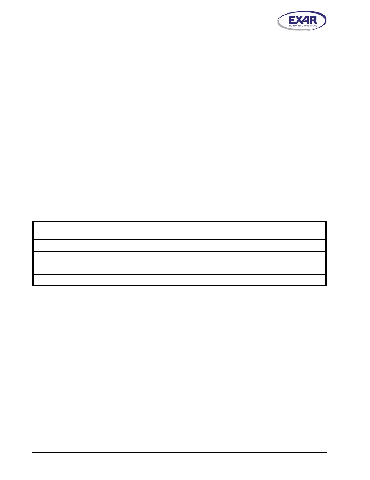
Table 5 below explains this.
T
ABLE
5: A
UTO XON/XOFF
RX T
RIGGER LEVEL
8 8 8* 0
16 16 16* 8
56 56 56* 16
60 60 60* 56
* After the trigger level is reached, an xoff character is sent after a short span of time (= time required to send 2 characters);
for example, after 2.083ms has elapsed for 9600 baud and 10-bit word length setting.
INT PIN A
CTIVATION
(S
OFTWARE
X
OFF CHARACTER(S
CHARACTERS IN RX FIFO
(
) F
) S
LOW CONTROL
ENT
)
XON C
HARACTER(S
CHARACTERS IN RX FIFO
(
) S
ENT
)
2.14 Special Character Detect
A special character detect feature is provided to detect an 8-bit character when bit-5 is set in the Enhanced
Feature Register (EFR). When this character (Xoff2) is detected, it will be placed in the FIFO along with normal
incoming RX data.
The M780 compares each incoming receive character with Xoff-2 data. If a match exists, the received data will
be transferred to the RX FIFO and ISR bit-4 will be set to indicate detection of special character. Although the
Internal Register Table shows Xon, Xoff Registers with eight bits of character information, the actual number of
bits is dependent on the programmed word length. Line Control Register (LCR) bits 0-1 defines the number of
character bits, i.e., either 5 bits, 6 bits, 7 bits, or 8 bits. The word length selected by LCR bits 0-1 also
determines the number of bits that will be used for the special character comparison. Bit-0 in the Xon, Xoff
Registers corresponds with the LSB bit for the receive character.
2.15 Normal Multidrop Mode
Normal multidrop mode is enabled when MSR[6] = 1 (requires EFR[4] = 1) and EFR[5] = 0 (Special Character
Detect disabled). The receiver is set to Force Parity 0 (LCR[5:3] = ’111’) in order to detect address bytes.
With the receiver initially disabled, it ignores all the data bytes (parity bit = 0) until an address byte is received
(parity bit = 1). This address byte will cause the UART to set the parity error. The UART will generate an LSR
20
Page 21

XR16M780
REV. 1.0.0
interrupt and place the address byte in the RX FIFO. The software then examines the byte and enables the
receiver if the address matches its slave address, otherwise, it does not enable the receiver.
If the receiver has been enabled, the receiver will receive the subsequent data. If an address byte is received,
it will generate an LSR interrupt. The software again examines the byte and if the address matches its slave
address, it does not have to do anything. If the address does not match its slave address, then the receiver
should be disabled.
2.15.1 Auto Address Detection
Auto address detection mode is enabled when MSR[6] = 1 (requires EFR[4] = 1) and EFR bit-5 = 1. The
desired slave address will need to be written into the XOFF2 register. The receiver will try to detect an address
byte that matches the porgr ammed character in the XOFF2 register. If the received byte is a data byte or an
address byte that does not match the programmed character in the XOFF2 register, the receiver will discard
these data. Upon receiving an address byte that matches the XOFF2 character, the receiver will be
automatically enabled if not already enabled, and the address character is pushed into the RX FIFO along with
the parity bit (in place of the parity er ror bit). The receiver also generates an LSR interrupt. The receiver will
then receive the subsequent data. If another address byte is received and this address does not match the
programmed XOFF2 character, then the receiver will automatically be disabled and the address byte is
ignored. If the address byte matches XOFF2 , the receiver wi ll put this byte in the RX FIFO along with the parity
bit in the parity error bit.
2.16 Infrared Mode
The M780 UART includes the infrared encode r and de coder compatible to the IrDA (Infrared Dat a Associ ation)
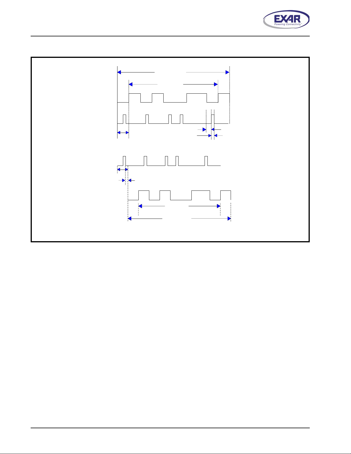
version 1.0 and 1.1. The IrDA 1.0 standard that stipulates the infrared encoder sends out a
HIGH-pulse for each “0” bit in the transmit data stream with a data rate up to 115.2 Kbps. For the IrDA 1.1
standard, the infrared encoder sends out a 1/4 of a bit time wide HIGH-pulse for each "0" bit in the transmit
data stream with a data rate up to 1.152 Mbps. This signal encoding reduces the on-time of the infrared LED,
hence reduces the power consumption. See
1.62V TO 3.63V HIGH PERFORMANCE UART WITH 64-BYTE FIFO
3/16 of a bit wide
Figure 14 below.
The infrared encoder and decoder are enabled by setting MCR register bit-6 to a ‘1’. With this bit enabled, the
infrared encoder and decoder is compatible to the IrDA 1.0 standard. For the infrared encoder and decoder to
be compatible to the IrDA 1.1 standard, MSR bit-7 will also need to be set to a ’1’ when EFR bit-4 is set to ’1’.
Likewise, the RX input assumes an idle level of logic zero from a reset an d power up, see
Typically, the wireless infrared decoder receives the input pulse from the infrared sensing diode on the RX pin.
Each time it senses a light pulse, it returns a logic 1 to the data bit stream.
Figure 14.
21
Page 22
XR16M780
1.62V TO 3.63V HIGH PERFORMANCE UART WITH 64-BYTE FIFO
F
IGURE
14. I
NFRARED TRANSMIT DATA ENCODING AND RECEIVE DATA DECODING
Character
Data Bits
3/16 or 1/4 Bit Time
TX Data
Transmit
IR Pulse
(TX Pin)
Receive
IR Pulse
(RX pin)
RX Data
Start
11 111
0000 0
Bit Time
Bit Time
1/16 Clock Delay
11 111
0000 0
REV. 1.0.0
Stop
1/2 Bit Time
IrEncoder-1
Start
Data Bits
Character
Stop
IRdecoder-1
2.17 Sleep Mode with Auto Wake-Up and Power-Save feature
The M780 supports low voltage system designs, hence, a sleep mode with auto wake-up and power-save
feature is included to reduce its power consumption when the chip is not actively used.
2.17.1 Sleep mode
All of these conditions must be satisfied for the M780 to enter sleep mode:
■
no interrupts pending (ISR bit-0 = 1)
■
sleep mode is enabled (IER bit-4 = 1)
■
modem inputs are not toggling (MSR bits 0-3 = 0)
■
RX input pin is idling HIGH in normal mode or LOW in infrared mode
■
divisor is non-zero
■
TX and RX FIFOs are empty
The M780 stops its crystal oscillator to conserve power in the sleep mode. User can check the XTAL2 pin for
no clock output as an indication that the device has entered the sleep mode.
The M780 resumes normal operation by any of the following:
■
a receive data start bit transition (HIGH to LOW)
■
a data byte is loaded to the transmitter, THR or FIFO
■
a change of logic state on any of the modem or general purpose serial inputs: CTS#, DSR#, CD#, RI#
If the M780 is awakened by any one of the above co nd itions, it will r et urn t o the sle ep mode au to mati cally after
all interrupting conditions have been se rviced and cleared. If the M780 is awakened by the modem inputs, a
read to the MSR is required to reset the modem inputs. In any case, the sleep mode will not be entered while
22
Page 23

XR16M780
REV. 1.0.0
1.62V TO 3.63V HIGH PERFORMANCE UART WITH 64-BYTE FIFO
an interrupt is pending from any channel. The M780 will stay in the sleep mode of operation until it is disabled
by setting IER bit-4 to a logic 0.
A word of caution: owing to the starting up delay of the crystal oscillator after waking up from sleep mode, the
first few receive characters may be lost. Also , make sure the RX pin is idling HIGH or “marking” condition
during sleep mode. This may not occur when the external interface transceivers (RS-232, RS-485 or another
type) are also put to sleep mode and cannot maint a in the “marking” condition. To avoid this, the system design
engineer can use a 47k ohm pull-up resistor on each of the RX input.
2.17.2 Power-Save Feature
If the address lines, data bus lines, IOW#, IOR#, CS# and modem input lines remain steady when the M780 is
in sleep mode, the maximum current will be in the microamp range as specified in the DC Electrical
Characteristics on
page 45. If the input lines are floating or are toggling while the M780 is in sleep mode, the
current can be up to 100 times more. If not using the Power- Save fe ature, an exte rnal buffer would be required
to keep the address and data bus lines from toggling or floating to achieve the low current. But if the PowerSave feature is enabled (PwrSave pin connected to VCC), this will eliminate the need for an external buffer by
internally isolating the address, data and control sign als (see
Figure 1 on page 1) from other bus activities that
could cause wasteful power drain. The M780 enter s Powe r-Save mode whe n this pin is con nected to VCC and
the M780 is in sleep mode (see Sleep Mode section above).
Since Power-Save mode isolates the address, data and control signals, the device will wake-up only by:
■
a receive data start bit transition (HIGH to LOW) at the RX input or
■
a change of logic state on the modem or general purpose serial input CTS#, DSR#, CD#, RI#
The M780 will return to the Power-Save mode automatically after a read to the MSR (to reset the modem input
CTS#) and all interrupting conditions have been serviced and cleared. The M780 will stay in the Power-Save
mode of operation until it is disabled by setting IER bit-4 t o a logic 0 a nd/or t he Powe r-Save pin is co nnect ed to
GND.
2.17.3 Wake-up Interrupt
The M780 has the wake up interrupt. By setting the FCR bit-3, wake up interrupt is enabled or disabled. The
default status of wake up interrupt is disabled. Please
See ”Section 4.5, FIFO Control Register (FCR) -
Write-Only” on page 31.
23
Page 24
XR16M780
1.62V TO 3.63V HIGH PERFORMANCE UART WITH 64-BYTE FIFO
REV. 1.0.0
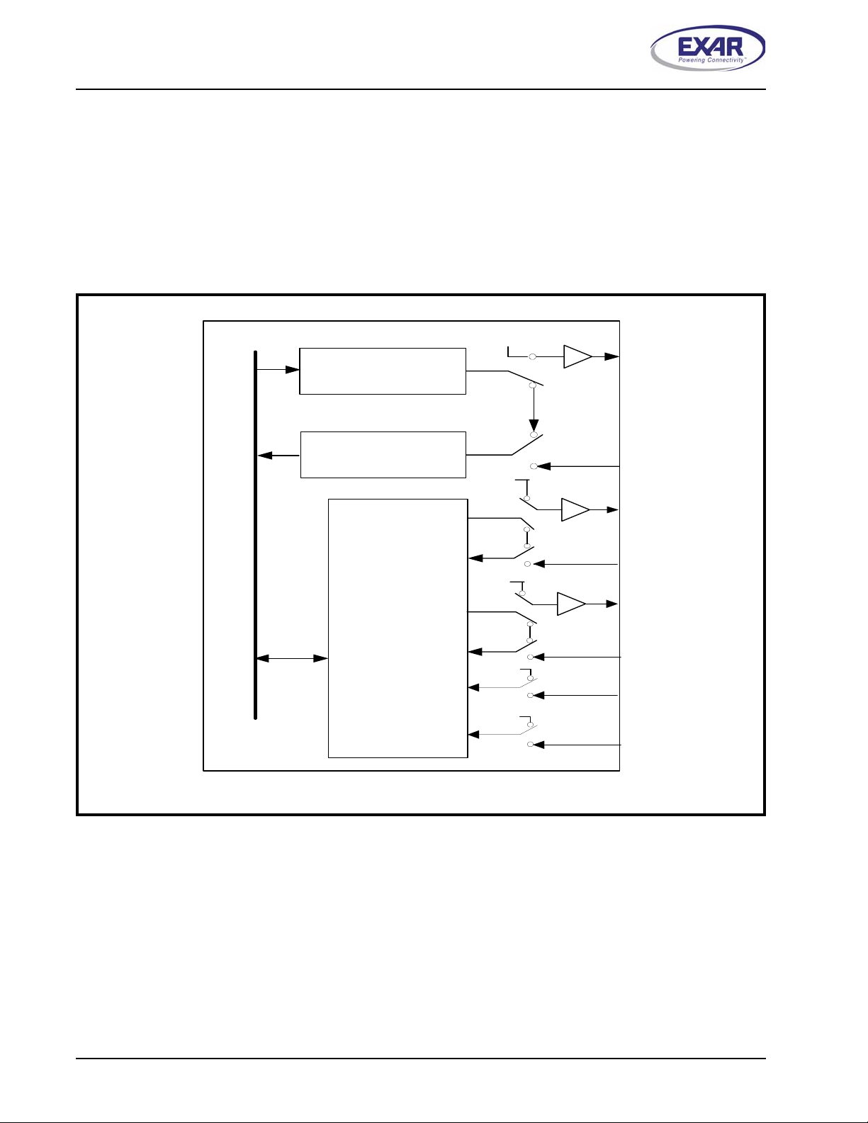
2.18 Internal Loopback
The M780 UART provides an internal loopback capability for system diagnostic purposes. The internal
loopback mode
normally.
is enabled by setting MCR register bit-4 to logic 1. All regular UART functions operate
Figure 15 shows how the modem port signals are re-configured . T ran smit dat a from the tr ansmit shif t
register output is internally routed to the receive shift register input allowing the system to receive the same
data that it was sending. The TX pin is held HIGH or mark condition while RTS# and DTR# are de-asserted,
and CTS#, DSR# CD# and RI# inputs are ignored. Caution: the RX input must be held HIGH during loopback
test else upon exiting the loopback test the UART may detect and report a false “break” signal.
F
IGURE
15. I
NTERNAL LOOPBACK
Tra n sm it Shift Registe r
(THR/FIFO)
Receive Shift Register
(RHR/FIFO)
VCC
TX
MCR bit-4=1
RX
VCC
Internal Data Bus Lines and Control Signals
RTS#
CTS#
VCC
DTR#
DSR#
OP1#
RI#
Modem / General Purpose Control Logic
CD#
OP2#
RTS#
CTS#
DTR#
DSR#
RI#
CD#
24
Page 25
XR16M780
REV. 1.0.0
1.62V TO 3.63V HIGH PERFORMANCE UART WITH 64-BYTE FIFO
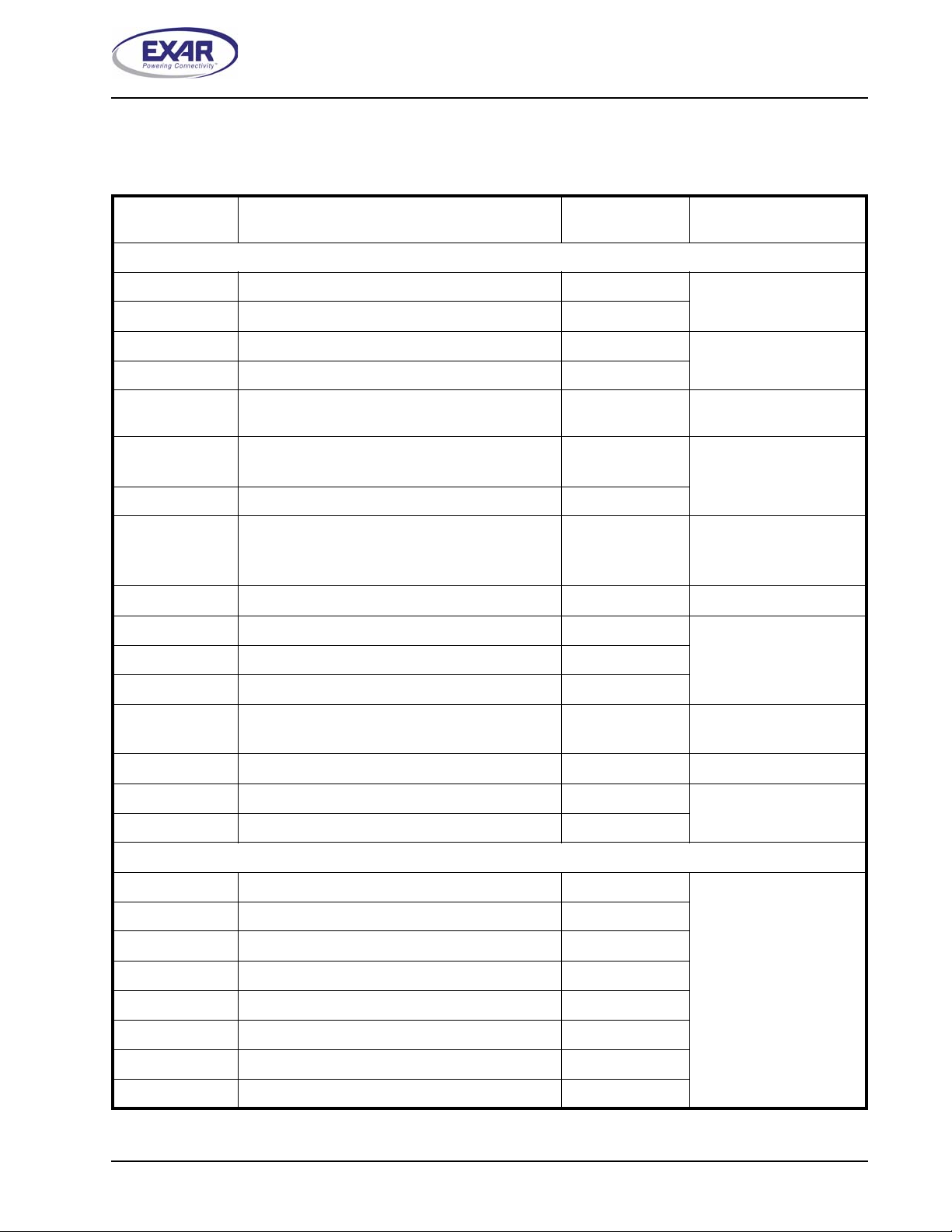
3.0 UART INTERNAL REGISTERS
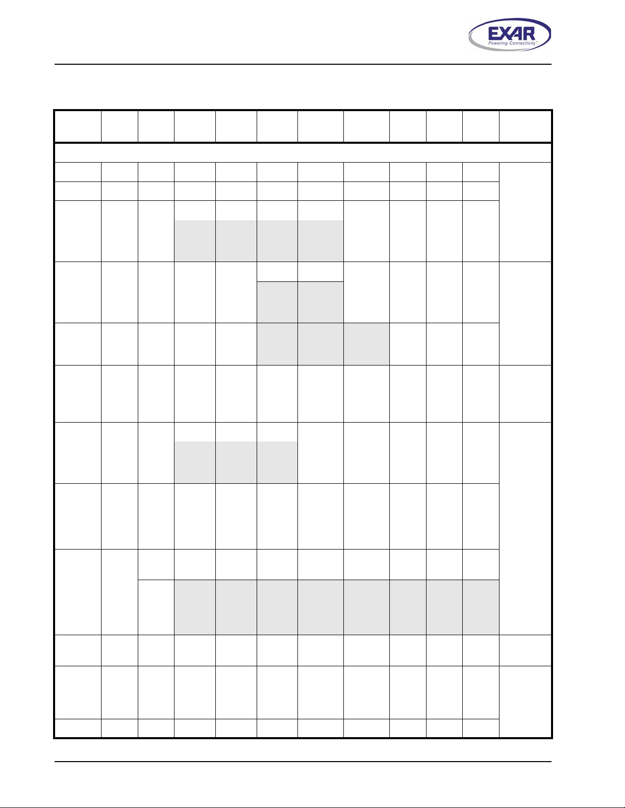
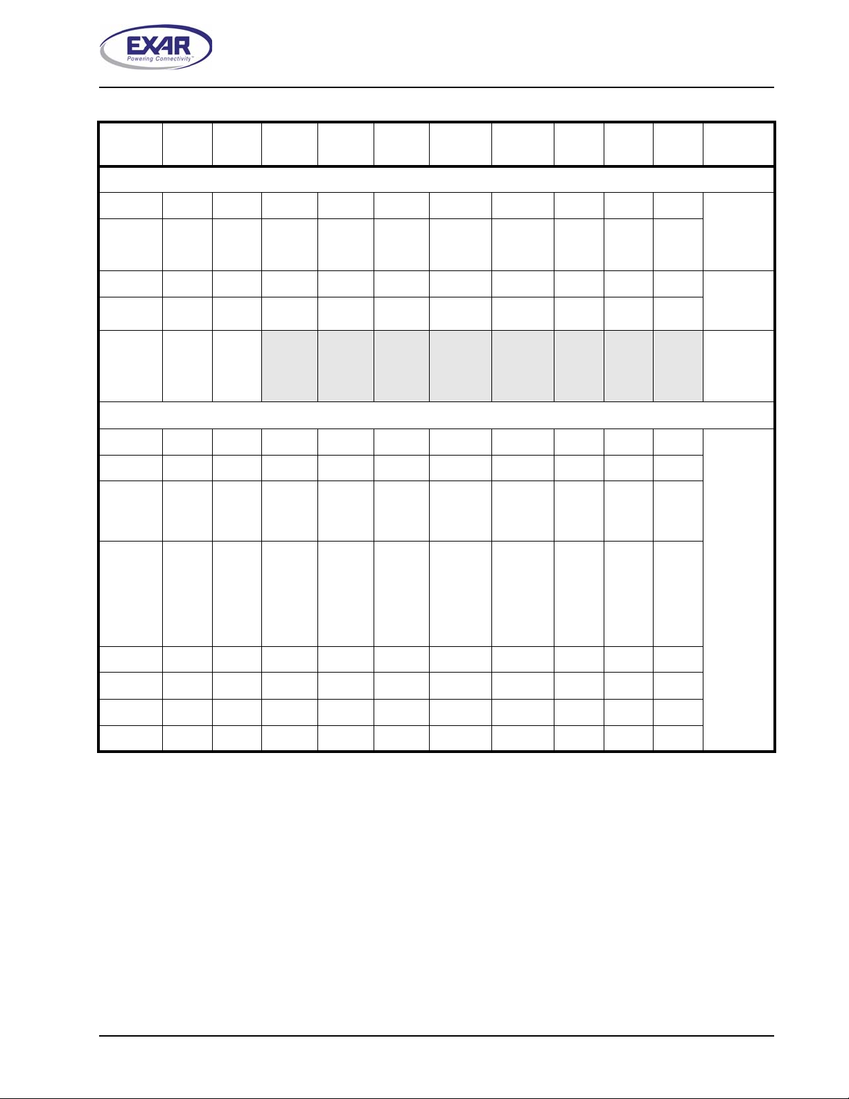
The complete register set for the M780 is shown in Table 6 and Table 7.
T
ABLE
6: UART INTERNAL REGISTERS
A2 A1 A0
A
DDRESSES
0 0 0 DREV - Device Revision Read-only
0 0 1 DVID - Device Identification Register Read-only
0 0 0 DLL - Divisor LSB Register Read/Write
0 0 1 DLM - Divisor MSB Register Read/Write
0 1 0 DLD - Divisor Fractional Register Read/Write LCR[7] = 1, LCR ≠ 0xBF,
0 0 0 RHR - Receive Holding Register
0 0 1 IER - Interrupt Enable Register Read/Write
0 1 0 ISR - Interrupt Status Register
THR - Transmit Holding Register
FCR - FIFO Control Register
R
EGISTER
16C550 C
OMPATIBLE REGISTERS
R
EAD/WRITE
Read-only
Write-only
Read-only
Write-only
C
OMMENTS
LCR[7] = 1, LCR ≠ 0xBF,
DLL = 0x00, DLM = 0x00
LCR[7] = 1, LCR ≠ 0xBF
See DLD[7:6]
EFR[4] = 1
LCR[7] = 0
LCR[7] = 0 if EFR[4] = 1
LCR ≠ 0xBF if EFR[4] = 0
or
0 1 1 LCR - Line Control Register Read/Write
1 0 0 MCR - Modem Control Register Read/Write
LCR ≠ 0xBF1 0 1 LSR - Line Status Register Read-only
1 1 0 MSR - Modem Status Register Read-only
1 1 0 MSR - Modem Status Register Write-only LCR ≠ 0xBF
EFR[4] = 1
1 1 1 SPR - Scratch Pad Register Read/Write LCR ≠ 0xBF, FCTR[6] = 0
1 1 1 EMSR - Enhanced Mode Select Register Write-only
1 1 1 FC - RX/TX FIFO Level Counter Register Read-only
E
NHANCED REGISTERS
0 0 0 FC - RX/TX FIFO Level Counter Register Read-only
0 0 0 TRIG - RX/TX FIFO Trigger Level Register Write-only
0 0 1 FCTR - Feature Control Register Read/Write
0 1 0 EFR - Enhanced Function Reg Read/Write
1 0 0 Xon-1 - Xon Character 1 Read/Write
1 0 1 Xon-2 - Xon Character 2 Read/Write
LCR ≠ 0xBF, FCTR[6] = 1
LCR = 0xBF
1 1 0 Xoff-1 - Xoff Character 1 Read/Write
1 1 1 Xoff-2 - Xoff Character 2 Read/Write
25
Page 26
XR16M780
1.62V TO 3.63V HIGH PERFORMANCE UART WITH 64-BYTE FIFO
T
ABLE
7: INTERNAL REGISTERS DESCRIPTION.
A
DDRESS
A2-A0
0 0 0 RHR RD Bit-7 Bit-6 Bit-5 Bit-4 Bit-3 Bit-2 Bit-1 Bit-0
0 0 0 THR WR Bit-7 Bit-6 Bit-5 Bit-4 Bit-3 Bit-2 Bit-1 Bit-0
0 0 1 IER RD/WR 0/ 0/ 0/ 0/ Modem
0 1 0 ISR RD FIFOs
0 1 0 FCR WR RX FIFO
R
N
EG
AME
W
R
EAD
RITE
/
BIT-7 BIT-6 BIT-5 BIT-4 BIT-3 BIT-2 BIT-1 BIT-0 C
16C550 Compatible Registers
CTS#
Int.
Enable
Enabled
RTS#
Int.
Enable
FIFOs
Enabled
Xoff Int.
Enable
0/ 0/ INT
RTS
CTS
Interrupt
Trigger
RX FIFO
Trigger
TX FIFO
Trigger
S
Sleep
Mode
Enable
Xoff
Interrupt
TX FIFO
Trigger
HADED BITS ARE ENABLED WHEN
Stat. Int.
Enable
Source
Bit-3
Wake up
Int Enable
RX Line
Stat.
Int.
Enable
INT
Source
Bit-2
TX
FIFO
Reset
TX
Empty
Int
Enable
INT
Source
Bit-1
RX
FIFO
Reset
REV. 1.0.0
EFR BIT-4=1
RX
LCR[7] = 0
Data
Int.
Enable
INT
Source
Bit-0
FIFOs
Enable
LCR[7] = 0
if EFR[4]=1
LCR≠0xBF
if EFR[4]=0
OMMENT
or
0 1 1 LCR RD/WR Divisor
Enable
1 0 0 MCR RD/WR 0/ 0/ 0/ Internal
BRG
Prescaler
1 0 1 LSR RD RX FIFO
Global
Error
1 1 0 MSR RD CD#
Input
WR Fast IR Enable
Set TX
Break
IR Mode
ENable
THR &
TSR
Empty
RI#
Input
9-bit
Set
Parity
XonAny
THR
Even
Parity
Lopback
Enable
RX Break RX Fram-
Empty
DSR#
Input
CTS#
Input
Disable RXDisable
TX
Parity
Enable
Stop
Bits
Word
Length
Bit-1
INT Out-
put
Enable
OP1# RTS#
Output
Control
(OP2#)
ing Error
RX
Parity
Error
RX
Over
run
Error
Delta
CD#
Delta
RI#
Delta
DSR#
0 0 0 0
-
Word
Length
Bit-0
DTR#
Output
Control
RX
Data
Ready
LCR≠0xBF
Delta
CTS#
mode
1 1 1 SPR RD/WR Bit-7 Bit-6 Bit-5 Bit-4 Bit-3 Bit-2 Bit-1 Bit-0 LCR≠0xBF
FCTR[6]=0
1 1 1 EMSR WR Xoff
interrupt
mode
select
LSR
interrupt
mode
select
RTS
delay bit-
3
RTS
delay bit-
2
Invert
RTS in
RS485
mode
Send
TX
imme
diate
-
FIFO
count
control
bit-1
FIFO
count
control
bit-0
1 1 1 FC RD Bit-7 Bit-6 Bit-5 Bit-4 Bit-3 Bit-2 Bit-1 Bit-0
26
LCR≠0xBF
FCTR[6]=1
Page 27
XR16M780
REV. 1.0.0
A
DDRESS
A2-A0
T
ABLE
7: INTERNAL REGISTERS DESCRIPTION.
R
EG
R
EAD
/
N
AME
W
RITE
BIT-7 BIT-6 BIT-5 BIT-4 BIT-3 BIT-2 BIT-1 BIT-0 C
1.62V TO 3.63V HIGH PERFORMANCE UART WITH 64-BYTE FIFO
S
HADED BITS ARE ENABLED WHEN
Baud Rate Generator Divisor
EFR BIT-4=1
OMMENT
0 0 0 DREV RD Bit-7 Bit-6 Bit-5 Bit-4 Bit-3 Bit-2 Bit-1 Bit-0 LCR[7] = 1
LCR≠0xBF
0 0 1 DVID RD 0 0 0 0 1 0 0 1
DLL= 0x00
DLM= 0x00
0 0 0 DLL RD/WR Bit-7 Bit-6 Bit-5 Bit-4 Bit-3 Bit-2 Bit-1 Bit-0 LCR[7] = 1
0 0 1 DLM RD/WR Bit-7 Bit-6 Bit-5 Bit-4 Bit-3 Bit-2 Bit-1 Bit-0
0 1 0 DLD RD/WR BRG
select
Enable
Indepen-
4X Mode 8X Mode Bit-3 Bit-2 Bit-1 Bit-0 LCR[7] = 1
dent
BRG
Enhanced Registers
LCR≠0xBF
DLD[7:6]
LCR≠0xBF
EFR[4] = 1
0 0 0 FC RD Bit-7 Bit-6 Bit-5 Bit-4 Bit-3 Bit-2 Bit-1 Bit-0
0 0 0 TRIG WR Bit-7 Bit-6 Bit-5 Bit-4 Bit-3 Bit-2 Bit-1 Bit-0
0 0 1 FCTR RD/WR RX/TX
select
0 1 0 EFR RD/WR Auto
CTS#
Enable
Swap
SCR
Auto
RTS#
Enable
trigger
mode
bit-1
Special
Char
Select
trigger
mode
bit-0
Enable
IER [7:4],
ISR [5:4],
FCR[5:3],
MCR[7:5],
DLD
RS485
interrupt
mode
Soft-
ware
Flow
Cntl
Bit-3
invert
RX IR
Software
Flow
Cntl
Bit-2
RTS
delay
bit-1
Soft-
ware
Flow
Cntl
Bit-1
1 0 0 XON1 RD/WR Bit-7 Bit-6 Bit-5 Bit-4 Bit-3 Bit-2 Bit-1 Bit-0
1 0 1 XON2 RD/WR Bit-7 Bit-6 Bit-5 Bit-4 Bit-3 Bit-2 Bit-1 Bit-0
1 1 0 XOFF1 RD/WR Bit-7 Bit-6 Bit-5 Bit-4 Bit-3 Bit-2 Bit-1 Bit-0
1 1 1 XOFF2 RD/WR Bit-7 Bit-6 Bit-5 Bit-4 Bit-3 Bit-2 Bit-1 Bit-0
4.0 INTERNAL REGISTER DESCRIPTIONS
4.1 Receive Holding Register (RHR) - Read- Only
SEE”RECEIVER” ON PAGE 16.
4.2 Transmit Holding Register (THR) - Write-Only
SEE”TRANSMITTER” ON PAGE 15.
RTS
delay
bit-0
Soft-
ware
Flow
Cntl
Bit-0
LCR=0XBF
27
Page 28

XR16M780
1.62V TO 3.63V HIGH PERFORMANCE UART WITH 64-BYTE FIFO
4.3 Interrupt Enable Register (IER) - Read/Write
The Interrupt Enable Register (IER) masks the interrupts from receive data ready, transmit empty, line status
and modem status registers. These interrupts are reported in the Interrupt Status Register (ISR).
4.3.1 IER versus Receive FIFO Interrupt Mode Operation
When the receive FIFO (FCR BIT-0 = 1) and receive interrupts (IER BIT-0 = 1) are enabled, the RHR interrupts
(see ISR bits 2 and 3) status will reflect the following:
A. The receive data available interrupts are issued to the host when the FIFO has reached the programmed
trigger level. It will be cleared when the FIFO drops below the programmed trigger level.
B. FIFO level will be reflected in the ISR register when the FIFO trigger level is reached. Both the ISR register
status bit and the interrupt will be cleared when the FIFO drops below the trigger level.
C. The receive data ready bit ( LSR BIT-0) is set as soon as a character is transferred from the shift register t o
the receive FIFO. It is reset when the FIFO is empty.
4.3.2 IER versus Receive/Transmit FIFO Polled Mode Operation
When FCR BIT-0 equals a logic 1 for FIFO enable; resetting IER bits 0-3 enables the XR16M780 in the FIFO
polled mode of operation. Since the receiver and transmitter have separate bits in the LSR either or both can
be used in the polled mode by selecting respective transmit or receive control bit(s).
A. LSR BIT-0 indicates there is data in RHR or RX FIFO.
B. LSR BIT-1 indicates an overrun error has occurred and that data in the FIFO may not be valid.
C. LSR BIT 2-4 provides the type of receive data errors encountered for the data byte in RHR, if any.
D. LSR BIT-5 indicates THR is empty.
E. LSR BIT-6 indicates when both the transmit FIFO and TSR are empty.
F. L SR BIT-7 indicates a data error in at least one character in the RX FIFO.
REV. 1.0.0
IER[0]: RHR Interrupt Enable
The receive data ready interrupt will be issued when RHR has a dat a cha ract er in th e no n- FIF O mode or when
the receive FIFO has reached the programmed trigger level in the FIFO mode.
Logic 0 = Disable the receive data ready interrupt (default).
Logic 1 = Enable the receiver data ready interrupt.
IER[1]: THR Interrupt Enable
This bit enables the Transmit Ready interrupt which is issued whenever the THR becomes empty in the nonFIFO mode or when data in the FIFO falls below the programmed trigger level in the FIFO mode. If the THR is
empty when this bit is enabled, an interrupt will be generated.
Logic 0 = Disable Transmit Ready interrupt (default).
Logic 1 = Enable Transmit Ready interrupt.
IER[2]: Receive Line Status Interrupt Enable
If any of the LSR register bits 1, 2, 3 o r 4 is a logic 1, it will generate an interrupt to inform the host controller
about the error status of the current data byte in FIFO. LSR bit-1 generates an interrupt immediately when an
overrun occurs. LSR bits 2-4 generate an interrupt when the character in the RHR has an error. However,
when EMSR bit-6 changes to 1 (default is 0), LSR bit 2-4 generate an interrupt when the character is received
in the RX FIFO. Please refer to
page 38.
•
Logic 0 = Disable the receiver line status interrupt (default).
“Section 4.12, Enhanced Mode Select Register (EMSR) - Write-only” on
•
Logic 1 = Enable the receiver line status interrupt.
28
Page 29

XR16M780
REV. 1.0.0
IER[3]: Modem Status Interrupt Enable
•
Logic 0 = Disable the modem status register interrupt (default).
•
Logic 1 = Enable the modem status register interrupt.
IER[4]: Sleep Mode Enable (requires EFR[4] = 1)
•
Logic 0 = Disable Sleep Mode (default).
•
Logic 1 = Enable Sleep Mode. See Sleep Mode section for further details.
IER[5]: Xoff Interrupt Enable (requires EFR[4]=1)
•
Logic 0 = Disable the software flow control, receive Xoff interrupt. (default)
•
Logic 1 = Enable the software flow control, receive Xoff interrupt. See Software Flow Control section for
details.
IER[6]: RTS# Output Interrupt Enable (requires EFR[4]=1)
•
Logic 0 = Disable the RTS# interrupt (default).
•
Logic 1 = Enable the RTS# interrupt. The UART issues an interrupt when the RTS# pin makes a transition
from LOW to HIGH (if enabled by EFR bit-6).
IER[7]: CTS# Input Interrupt Enable (requires EFR[4]=1)
•
Logic 0 = Disable the CTS# interrupt (default).
1.62V TO 3.63V HIGH PERFORMANCE UART WITH 64-BYTE FIFO
•
Logic 1 = Enable the CTS# interrupt. The UART issues an interrupt when CTS# pin makes a transition from
LOW to HIGH (if enabled by EFR bit-7).
4.4 Interrupt Status Register (ISR) - Read-Only
The UART provides multiple levels of prioritized interrupts to minimize external software interaction. The
Interrupt Status Register (ISR) provides the user with six inter rupt status bits. Performing a read cycle on the
ISR will give the user the current highest pending interrupt level to be serviced, others are queued up to be
serviced next. No other interrupts are acknowledged until the pending interrupt is serviced. The Interrupt
Source Table,
associated with each of these interrupt levels.
4.4.1 Interrupt Generation:
•
LSR is by any of the LSR bits 1, 2, 3 and 4.
•
RXRDY is by RX trigger level.
•
RXRDY Time-out is by a 4-char plus 12 bits delay timer.
•
TXRDY is by TX trigger level or TX FIFO empty.
•
MSR is by any of the MSR bits 0, 1, 2 and 3.
•
Receive Xon/Xoff/Special character is by detection of a Xon, Xoff or Special character.
•
CTS# is when the remote transmitter toggle s the input pin (fr om LOW to HIGH) during au to CTS flow control.
•
RTS# is when its receiver toggles the output pin (from LOW to HIGH) during auto RTS flow control.
•
Wakeup interrupt is generated when the M780 wakes up from the sleep mode.
Table 8, shows the data values (bit 0-5) for the interrupt priority levels and the interrupt sources
29
Page 30
XR16M780
1.62V TO 3.63V HIGH PERFORMANCE UART WITH 64-BYTE FIFO
REV. 1.0.0
4.4.2 Interrupt Clearing:
•
LSR interrupt is cleared by a read to the LSR register.
•
RXRDY interrupt is cleared by reading data until FIFO falls below the t rigger level.
•
RXRDY Time-out interrupt is cleared by reading RHR.
•
TXRDY interrupt is cleared by a read to the ISR register or writing to THR.
•
MSR interrupt is cleared by a read to the MSR register.
•
Xon or Xoff interrupt is cleared by a read to the ISR register. See EMSR[7].
•
Special character interrupt is cleared by a read to ISR register or after next character is received. See
EMSR[7].
•
RTS# and CTS# flow control interrupts are cleared by a read to the MSR register.
•
Wakeup interrupt is cleared by a read to ISR register.
]
T
ABLE
8: I
NTERRUPT SOURCE AND PRIORITY LEVEL
P
RIORITY
L
EVEL
1 0 0 0 1 1 0 LSR (Receiver Line Status Register)
BIT-5 BIT-4 BIT-3 BIT-2 BIT-1 BIT-0
ISR R
EGISTER STATUS BITS
S
OURCE OF INTERRUPT
2 0 0 1 1 0 0 RXRDY (Receive Data Time-out)
3 0 0 0 1 0 0 RXRDY (Received Data Ready)
4 0 0 0 0 1 0 TXRDY (Transmit Ready)
5 0 0 0 0 0 0 MSR (Modem Status Register)
6 0 1 0 0 0 0 RXRDY (Received Xon, Xoff or Special character)
7 1 0 0 0 0 0 CTS#, RTS# change of state
- 0 0 0 0 0 1 None (default) or Wakeup interrupt
ISR[0]: Interrupt Status
•
Logic 0 = An interrupt is pending and the ISR contents may be used as a pointer to the appropriate interrupt
service routine.
•
Logic 1 = No interrupt pending (default condition).
ISR[3:1]: Interrupt Status
These bits indicate the source for a pe ndi ng interr upt at inter rupt pr iori ty levels (See Inter rupt Sour ce Table 8).
ISR[4]: Interrupt Status (requires EFR bit-4 = 1)
This bit is enabled when EFR bit-4 is set to a logic 1. ISR bit-4 indicates that the receiver detected a data
match of the Xoff, Xon or special character(s).
ISR[5]: Interrupt Status (requires EFR bit-4 = 1)
ISR bit-5 indicates that CTS# or RTS# has changed state from LOW to HIGH.
ISR[7:6]: FIFO Enable Status
These bits are set to a logic 0 when the FIFOs are disabled. They are set to a logic 1 when the FIFOs are
enabled.
30
Page 31

XR16M780
REV. 1.0.0
4.5 FIFO Control Register (FCR) - Write-Only
This register is used to enable the FIFOs, clear the FIFOs, set the transmit/receive FIFO trigger levels, and
enable the wake up interrupt. They are defined as follows:
FCR[0]: TX and RX FIFO Enable
•
Logic 0 = Disable the transmit and receive FIFO (default).
•
Logic 1 = Enable the transmit and receive FIFOs. This bit must be set to logic 1 when other FCR bits are
written or they will not be programmed.
FCR[1]: RX FIFO Reset
This bit is only active when FCR bit-0 is a ‘1’.
•
Logic 0 = No receive FIFO reset (default)
•
Logic 1 = Reset the receive FIFO pointers and FIFO level counter logic (the receive shift register is not
cleared or altered). This bit will return to a logic 0 after resetting the FIFO.
FCR[2]: TX FIFO Reset
This bit is only active when FCR bit-0 is a ‘1’.
•
Logic 0 = No transmit FIFO reset (default).
•
Logic 1 = Reset the transmit FIFO pointers and FIFO level counter logic (the transmit shift register is not
cleared or altered). This bit will return to a logic 0 after resetting the FIFO.
1.62V TO 3.63V HIGH PERFORMANCE UART WITH 64-BYTE FIFO
FCR[3]: Enable wake up interrupt (requires EFR bit-4 = 1)
•
Logic 0 = Disable the wake up interrupt (default).
•
Logic 1 = Enable the wake up interrupt.
Please refer to “Section 2.17.3, Wake-up Interrupt” on page 23.
FCR[5:4]: Transmit FIFO Trigger Select (requires EFR bit-4 = 1)
These 2 bits set the trigger level for the transm it FIFO. The UART will issue a transmit interrupt when the
number of characters in the FIFO falls below the selected trigger level, or when it gets empty in case that the
FIFO did not get filled over the trigger level on last re-load.
receiver and the transmitter cannot use different trigger tables. Whichever selection is made last applies to
both the RX and TX side.
FCR[7:6]: Receive FIFO Trigger Select
These 2 bits are used to set the trigger level for the receive FIFO. The UART will issue a receive interrupt when
the number of the characters in th e FIFO crosses the trigger level.
Note that the receiver and the transmitter cannot use different trigger tables. Whichever selection is made last
applies to both the RX and TX side.
Table 9 below shows the selections. Note that the
Table 9 shows the complete selections.
31
Page 32
XR16M780
1.62V TO 3.63V HIGH PERFORMANCE UART WITH 64-BYTE FIFO
T
ABLE
9: T
T
RIGGER
ABLE
T
Table-A
Table-B
Table-C
FCTR
BIT-5
0 0
0 1
1 0
FCTR
BIT-4
RANSMIT AND RECEIVE
FCR
BIT-7
FCR
BIT-6
0
0
1
1
0
0
1
1
0
0
1
1
0
1
0
1
0
1
0
1
0
1
0
1
FIFO T
FCR
BIT-5
0 0
0
0
1
1
0
0
1
1
RIGGER TABLE AND LEVEL SELECTION
FCR
BIT
-4
R
ECEIVE
RIGGER LEVEL
T
1 (default)
4
8
14
0
1
0
1
8
16
24
28
0
1
0
1
8
16
56
60
REV. 1.0.0
T
RANSMIT
RIGGER
T
L
EVEL
C
OMPATIBILITY
1 (default) 16C550, 16C2550,
16C2552, 16C554,
16C580
16
16C650A
8
24
30
8
16C654
16
32
56
Table-D
1 1 X X X X Programmable
via TRG
register.
FCTR[7] = 0.
Programmable
via TRG
register.
FCTR[7] = 1.
16L2752, 16C2850,
16C2852, 16C850,
16C854, 16C864
4.6 Line Control Register (LCR) - Read/Write
The Line Control Register is used to specify the asynchronous data communication format. The word or
character length, the number of stop bits, and the parity are selected by writing the appropriate bits in this
register.
LCR[1:0]: TX and RX Word Length Select
These two bits specify the word length to be transmitted or received.
BIT-1 BIT-0 W
0 0 5 (default)
0 1 6
1 0 7
1 1 8
ORD LENGTH
32
Page 33
XR16M780
REV. 1.0.0
1.62V TO 3.63V HIGH PERFORMANCE UART WITH 64-BYTE FIFO
LCR[2]: TX and RX Stop-bit Length Select
The length of stop bit is specified by this bit in conjunction with the programmed word length.
S
W
ORD
BIT-2
0 5,6,7,8 1 (default)
1 5 1-1/2
1 6,7,8 2
LENGTH
TOP BIT LENGTH
(BIT
TIME(S
))
LCR[3]: TX and RX Parity Select
Parity or no parity can be selected via this bit. The parity bit is a simple way used in communications for data
integrity check. See
•
Logic 0 = No parity.
•
Logic 1 = A parity bit is generated during the transmission while the receiver checks for parity error of the
Table 10 for parity selection summary below.
data character received.
LCR[4]: TX and RX Parity Select
If the parity bit is enabled with LCR bit-3 set to a logic 1, LCR BIT-4 selects the even or odd parity format.
•
Logic 0 = ODD Parity is generated by forcing an odd number of logic 1’s in the transmitted character. The
receiver must be programmed to check the same format (default).
•
Logic 1 = EVEN Parity is generated by forcing an even number of logic 1’s in the transmitted character. The
receiver must be programmed to check the same format.
LCR[5]: TX and RX Parity Select
If the parity bit is enabled, LCR BIT-5 selects the forced parity format.
•
LCR BIT-5 = logic 0, parity is not forced (default).
•
LCR BIT-5 = logic 1 and LCR BIT-4 = logic 0, parity bit is forced to a logical 1 for the transmit and receive
data.
•
LCR BIT-5 = logic 1 and LCR BIT-4 = logic 1, parity bit is forced to a logical 0 for the transmit and receive
data.
T
ABLE
10: P
ARITY SELECTION
LCR BIT-5 LCR BIT-4 LCR BIT-3 P
X X 0 No parity
0 0 1 Odd parity
0 1 1 Even parity
1 0 1 Force parity to mark, HIGH
ARITY SELECTION
1 1 1 Forced parity to space, LOW
33
Page 34

XR16M780
1.62V TO 3.63V HIGH PERFORMANCE UART WITH 64-BYTE FIFO
LCR[6]: Transmit Break Enable
When enabled, the Break control bit causes a break condition to be transmitted (the TX output is forced to a
“space’, logic 0, state). This condition remains, until disabled by setting LCR bit-6 to a logic 0.
•
Logic 0 = No TX break condition. (default)
•
Logic 1 = Forces the transmitter output (TX) to a “space”, logic 0, for alerting the remote receiver of a line
break condition.
LCR[7]: Baud Rate Divisors Enable
Baud rate generator divisor (DLL/DLM/DLD) enable.
•
Logic 0 = Data registers are selected. (default)
•
Logic 1 = Divisor latch registers are selected.
4.7 Modem Control Register (MCR) or General Purpose Outputs Control - Read/Write
The MCR register is used for controlling the serial/modem interface signals or general purpose inputs/outputs.
MCR[0]: DTR# Output
The DTR# pin is a modem control output. If the modem interface is not used, this output may be used as a
general purpose output.
•
Logic 0 = Force DTR# output HIGH (default).
REV. 1.0.0
•
Logic 1 = Force DTR# output LOW.
MCR[1]: RTS# Output
The RTS# pin is a modem control output and may be used for automatic hardware flow control by enabled by
EFR bit-6. If the modem interface is not used, this output may be used as a general purpose output.
•
Logic 0 = Force RTS# output HIGH (default).
•
Logic 1 = Force RTS# output LOW. It is required to start Auto RTS Flow Control.
MCR[2]: Reserved
OP1# is not available as an output pin on the M780. But it is available for use during Internal Loopback Mode.
In the Loopback Mode, this bit is used to write the state of the modem RI# interface signal.
MCR[3]: INT Output Enable
Enable or disable INT outputs to become active or in three-state. This bit is also used to control the OP2#
signal during internal loopback mode.
•
Logic 0 = INT output disabled (three state) in the 16 mode (default). During internal loopback mode, OP2# is
HIGH.
•
Logic 1 = INT output enabled (active) in the 16 mode. During internal loopback mode, OP2# is LOW.
T
ABLE
MCR
BIT-3
11: INT O
INT O
UTPUT MODES
UTPUT IN
16 M
ODE
0 Three-State
1 Active
34
Page 35

XR16M780
REV. 1.0.0
MCR[4]: Internal Loopback Enable
•
Logic 0 = Disable loopback mode (default).
•
Logic 1 = Enable local loopback mode, see loopback section and Figure 15.
MCR[5]: Xon-Any Enable (requires EFR bit-4 = 1)
•
Logic 0 = Disable Xon-Any function (for 16C550 compatibility, default).
•
Logic 1 = Enable Xon-Any function. In this mode, any RX character received will resume transmit operation.
The RX character will be loaded into the RX FIFO , unless the RX character is an Xon or Xoff character and
the M780 is programmed to use the Xon/Xoff flow control.
MCR[6]: Infrared Encoder/Decoder Enable (requires EFR bit-4 = 1)
•
Logic 0 = Enable the standard modem receive and transmit input/output interface. (Default)
•
Logic 1 = Enable infrared IrDA receive and transmit inputs/outputs. The TX/RX ou tp ut / inpu t ar e ro ut ed t o the
infrared encoder/decoder. The data input and output levels conform to the IrDA infrared interface
requirement. The RX FIFO may need to be flushed upon enable. While in this mode, the infrared TX output
will be LOW during idle data conditions.
MCR[7]: Clock Prescaler Select (requires EFR bit-4 = 1)
•
Logic 0 = Divide by one. The input clock from the crysta l or external clock is fed directly to the Pr ogrammabl e
Baud Rate Generator without further modification, i.e., divide by one (default).
1.62V TO 3.63V HIGH PERFORMANCE UART WITH 64-BYTE FIFO
•
Logic 1 = Divide by four. The prescaler divides the input clock from the crystal or external clock by four and
feeds it to the Programmable Baud Rate Generator, hence, data rates become one forth.
4.8 Line Status Register (LSR) - Read Only
This register provides the status of dat a tran sfers betw een the UART and the host. If IER bit-2 is en abled, LSR
bit 1 will generate an interrupt immediately and LSR bits 2-4 will generate an interrupt when a character with an
error is in the RHR.
LSR[0]: Receive Data Ready Indicator
•
Logic 0 = No data in receive holding register or FIFO (default).
•
Logic 1 = Data has been received and is saved in the receive holding register or FIFO.
LSR[1]: Receiver Overrun Flag
•
Logic 0 = No overrun error (default).
•
Logic 1 = Overrun error. A data overrun error condition occurred in the receive shift register. This happens
when additional data arrives while the FIFO is full. In this case the previous data in the receive shift register
is overwritten. Note that under this condition the data byte in the receive shift register is not transferred into
the FIFO, therefore the data in the FIFO is not co rr up te d by the er ro r.
LSR[2]: Receive Data Parity Error Tag
•
Logic 0 = No parity error (default).
•
Logic 1 = Parity error. The receive character in RHR does not have correct parity information and is suspect.
This error is associated with the character available for reading in RHR.
LSR[3]: Receive Data Framing Error Tag
•
Logic 0 = No framing error (default).
•
Logic 1 = Framing error. The receive character did not have a valid stop bit(s). This error is associated with
the character available for reading in RHR.
35
Page 36

XR16M780
1.62V TO 3.63V HIGH PERFORMANCE UART WITH 64-BYTE FIFO
LSR[4]: Receive Break Tag
•
Logic 0 = No break condition (default).
•
Logic 1 = The receiver received a break signal (RX was LOW for at least one character fr ame time). In the
FIFO mode, only one break character is loaded into the FIFO. The break indication remains until the RX
input returns to the idle condition, “mark” or HIGH.
LSR[5]: Transmit Holding Register Empty Flag
This bit is the Transmit Holding Re gister Empty indi cator. The THR bit is set to a logic 1 when the last data byte
is transferred from the transmit holding register to the transmit shift register. The bit is reset to logic 0
concurrently with the data loading to the transmit holding register by the host. In the FIFO mode this bit is set
when the transmit FIFO is empty, it is cleared when the transmit FIFO contains at least 1 byte.
LSR[6]: THR and TSR Empty Flag
This bit is set to a logic 1 whenever the transmitter goes idle. It is set to logic 0 whenever either the THR or
TSR contains a data character. In the FIFO mode this bit is set to a logic 1 whenever the transmit FIFO and
transmit shift register are both empty.
LSR[7]: Receive FIFO Data Error Flag
•
Logic 0 = No FIFO error (default).
•
Logic 1 = A global indicator for the sum of all error bit s in t he RX FIFO. At least one p ar ity err or, framing error
or break indication is in the FIFO data. This bit clears when there is no more error(s) in any of the bytes in the
RX FIFO.
4.9 Modem Status Register (MSR) - Read Only
REV. 1.0.0
This register provides the current st at e of t he mod em inte rface input signals. Lower four bits of t his regist er are
used to indicate the changed information. These bits are set to a logic 1 whenever a signal from the modem
changes state. These bits may be used for general purpose inputs when they are not used with modem
signals. Reading the higher four bits shows the status of the modem signals.
MSR[0]: Delta CTS# Input Flag
•
Logic 0 = No change on CTS# input (default).
•
Logic 1 = The CTS# input has changed state since the last time it was monitored. A modem status interrupt
will be generated if MSR interrupt is enabled (IER bit-3).
MSR[1]: Delta DSR# Input Flag
•
Logic 0 = No change on DSR# input (default).
•
Logic 1 = The DSR# input has changed state since the last time it was mo nitored. A mo dem status interr upt
will be generated if MSR interrupt is enabled (IER bit-3).
MSR[2]: Delta RI# Input Flag
•
Logic 0 = No change on RI# input (default).
•
Logic 1 = The RI# input has changed from LOW to HIGH, ending of the ringing signal. A modem status
interrupt will be generated if MSR interrupt is enabled (IER bit-3).
MSR[3]: Delta CD# Input Flag
•
Logic 0 = No change on CD# input (default).
•
Logic 1 = Indicates that the CD# input has changed state since the last time it was monitored. A modem
status interrupt will be generated if MSR interrupt is enabled (IER bit-3).
36
Page 37

XR16M780
REV. 1.0.0
MSR[4]: CTS Input Status
CTS# pin may function as automatic hardware flow control signal input if it is enabled and selected by Auto
CTS (EFR bit-7). Auto CTS Flow Control allows starting and stopping of local data transmissions based on the
modem CTS# signal. A HIGH on the CTS# pin will stop UAR T tr ansmit ter as soon as the cur rent ch aracter h as
finished transmission, and a LOW will resume data transmission. Normally MSR bit-4 bit is the complement of
the CTS# input. However in the loopback mode, this bit is equivalent to the RTS# bit in the MCR register. The
CTS# input may be used as a general purpose input when the modem interface is not used.
MSR[5]: DSR Input Status
Normally this bit is the complement of the DSR# input. In the loopback mode, this bit is equiva len t to th e DTR#
bit in the MCR register. The DSR# input may be used as a general purpose input when the modem interface is
not used.
MSR[6]: RI Input Status
Normally this bit is the complement of the RI# input. In the loopback mode this bit is equivalent to bit-2 in th e
MCR register. The RI# input may be used as a general purpose input when the modem interfa ce is not us ed .
MSR[7]: CD Input Status
Normally this bit is the complement of the CD# inpu t. In the loopba ck mode th is bit is equivalen t to bit-3 in the
MCR register. The CD# input may be used as a general purpose input when the modem interfa ce is not us ed .
4.10 Modem Status Register (MSR) - Write Only
This register provides the advanced features of XR16M780. Lower four bits of this register are reserved.
Writing to the higher four bits enables additional functions.
1.62V TO 3.63V HIGH PERFORMANCE UART WITH 64-BYTE FIFO
MSR[3:0]: Reserved
MSR[4]: Enable/Disable Transmitter (Requires EFR[4] = 1)
•
Logic 0 = Enable Transmitter (default).
•
Logic 1 = Disable Transmitter.
MSR[5]: Enable/Disable Receiver (Requires EFR[4] = 1)
•
Logic 0 = Enable Receiver (default).
•
Logic 1 = Disable Receiver.
MSR[6]: Enable/Disable 9-bit mode (Requires EFR[4] = 1)
For the 9-bit mode information, See ”Section 2.15, Normal Multidrop Mode” on page 20.
•
Logic 0 = Normal 8-bit mode (default).
•
Logic 1 = Enable 9-bit or Multidrop mode.
MSR[7]: Enable/Disable fast IR mode (Requires EFR[4] = 1)
The M780 supports the new fast IR transmission with data rate up to 1.152 Mbps.
•
Logic 0 = IrDA version 1.0, 3/16 pulse ratio, data rate up to 115.2 Kbps (default).
•
Logic 1 = IrDA version 1.1, 1/4 pulse ratio, dat a rate up to 1 .152 Mbp s. For more IR mode information, please
See ”Section 2.16, Infrared Mode” on page 21.
4.11 Scratch Pad Register (SPR) - Read/Write
This is a 8-bit general purpose register for the user to store temporary data. The content of this register is
preserved during sleep mode but becomes 0xFF (default) after a reset or a power off-on cycle.
37
Page 38
XR16M780
1.62V TO 3.63V HIGH PERFORMANCE UART WITH 64-BYTE FIFO
REV. 1.0.0
4.12 Enhanced Mode Select Register (EMSR) - Write-only
This register replaces SPR (during a Write) and is accessible only when FCTR[6] = 1.
EMSR[1:0]: Receive/Transmit FIFO Level Count
When Scratchpad Swap (FCTR[6]) is asserted, EMSR bits 1-0 controls what mode the FIFO Level Co unter is
operating in.
T
ABLE
12: S
CRATCHPAD SWAP SELECTION
FCTR[6] EMSR[1] EMSR[0]
0 X X
1 X 0
1 0 1
1 1 1
Scratchpad is
Scratchpad
RX FIFO Level Counter Mode
TX FIFO Level Counter Mode
Alternate RX/TX FIFO Counter Mode
During Alternate RX/TX FIFO Level Counter Mode, the first value read after EMSR bits 1-0 have been
asserted will always be the RX FIFO Level Counter. The second value read will correspond with the TX FIFO
Level Counter. The next value will be the RX FIFO Level Counter again, then the TX FIFO Level Counter and
so on and so forth.
EMSR[2]: Send TX Immediately
•
Logic 0 = Do not send TX immediately (default).
•
Logic 1 = Send TX immediately. When FIFO is enabled and this bit is set, the next data will be written to the
TX shift register. Thus, the data will be sent out immediately instead of queuing in the FIFO. Every time, only
1 byte will be send out. Once this byte has been sent out, the EMSR[2] will go back to 0 automatically. If
more than 1 byte will be sent out, EMSR[2] needs to be set to 1 for each byte.
EMSR[3]: Invert RTS in RS485 mode
•
Logic 0 = RTS# output is a logic 0 during TX and a logic 1 during RX (default).
•
Logic 1 = RTS# output is a logic 1 during TX and a logic 0 during RX.
38
Page 39
XR16M780
REV. 1.0.0
EMSR[5:4]: Extended RTS Hysteresis
T
EMSR
BIT-5
0
0
0
0
0
0
0
0
1
1
1
1
1
1
1
1
1.62V TO 3.63V HIGH PERFORMANCE UART WITH 64-BYTE FIFO
ABLE
13: A
UTO
EMSR
BIT-4
0
0
0
0
1
1
1
1
0
0
0
0
1
1
1
1
RTS H
FCTR
BIT-1
0
0
1
1
0
0
1
1
0
0
1
1
0
0
1
1
YSTERESIS
FCTR
BIT-0
0
1
0
1
0
1
0
1
0
1
0
1
0
1
0
1
RTS#
H
YSTERESIS
HARACTERS
(C
±4
±6
±8
±8
±16
±24
±32
±40
±44
±48
±52
±12
±20
±28
±36
)
0
EMSR[6]: LSR Interrupt Mode
•
Logic 0 = LSR Interrupt Delayed (default). LSR bits 2, 3, and 4 will generate an interrupt when the character
with the error is in the RHR.
•
Logic 1 = LSR Interrupt Immediate. LSR bits 2, 3, and 4 will generate an inte rrupt as soon a s the cha racter is
received into the FIFO.
EMSR[7]: Xoff/Special character Interrupt Mode Select
This bit selects how the Xoff and Special character interrupt is cleared. The XON interrupt can only be cleared
by reading the ISR register.
•
Logic 0 = Xoff interrupt is cleared by either reading ISR register or when an XON chara cter is received.
Special character interrupt is cleared by either reading ISR register or when next character is received.
(default).
•
Logic 1 = Xoff/Special character interrupt can only be cleared by reading the ISR register.
4.13 Baud Rate Generator Registers (DLL, DLM and DLD) - Read/Write
These registers make-up the value of the baud rate divisor. The M780 has different DLL, DLM and DLD for
transmitter and receiver. It provides more convenience for the transmitter and receiver to transmit data with
different rate. The M780 uses DLD[7:6] to select TX or RX. Then it provides DLD[5:0] to select the sampling
frequency and fractional baud rate divisor. The concatenation of the contents of DLM and DLL gives the 16-bit
divisor value. The value is added to DLD[3:0]/16 to achieve the fractional baud rate divisor. DLD must be
enabled via EFR bit-4 before it can be accessed. See
Table 14 below and See ”Section 2.7, Programmable
Baud Rate Generator with Fractional Divisor” on page 13.
39
Page 40
XR16M780
1.62V TO 3.63V HIGH PERFORMANCE UART WITH 64-BYTE FIFO
REV. 1.0.0
DLD[5:4]: Sampling Rate Select
These bits select the dat a sa mpli ng rat e. By def ault, t he d at a samp ling rat e is 16X. The ma ximum dat a rat e will
double if the 8X mode is selected and will quadruple if the 4X mode is selected. See
T
ABLE
14: S
AMPLING RATE SELECT
DLD[5] DLD[4] S
0 0 16X
0 1 8X
1 X 4X
Table 14 below.
AMPLING RATE
DLD[6]: Independent BRG enable
•
Logic 0 = The Transmitter and Receiver uses the same Baud Rate Generator. (default).
•
Logic 1 = The Transmitter and Receiver uses different Baud Rate Generators. Use DLD[7] for selecting
which baud rate generator to configure.
DLD[7]: BRG select
When DLD[6] = 1, this bit selects whether the values written t o DLL , DLM and DL D[5:0 ] will be fo r t he Transmit
Baud Rate Generator or the Receive Ba ud Rate Generator. When DLD[6] = 0 (same Baud Rate Generator
used for both TX and RX), this bit must be a logic 0 to properly write to the appropriate DLL, DLM and
DLD[5:0]. .
T
ABLE
15: BRG S
DLD[7] DLD[6] BRG
0 0 Transmitter and Receiver uses same BRG.
Writing to DLL, DLM and DLD[5:0] configures the BRG for both the TX and RX.
0 1 Transmitter and Receiver uses different BRGs.
Writing to DLL, DLM and DLD[5:0] configures the BRG for TX.
1 1 Transmitter and Receiver uses different BRGs.
Writing to DLL, DLM and DLD[5:0] configures the BRG for RX.
1 0 Transmitter and Receiver uses same BRG.
Writing to DLL, DLM and DLD[5:0] has no effect on BRG used by the TX and RX.
ELECT
4.14 Trigger Level Register (TRG) - Write-Only
User Programmable Transmit/Receive Trigger Level Register.
TRG[7:0]: Trigger Level Register
These bits are used to program desired trigger levels when trigger Table-D is s elected. FCTR bit-7 selects
between programming the RX Trigger Level (a logic 0) and the TX Trigger Level (a logic 1).
4.15 RX/TX FIFO Level Count Register (FC) - Read-Only
This register replaces SPR (during a read) and is accessible when FCTR[6] = 1. This register is also
accessible when LCR = 0xBF. It is suggested to read the FIFO Level Count Register at the Scratchpad
Register location when FCTR bit-6 = 1. See
Table 12.
40
Page 41
XR16M780
REV. 1.0.0
FC[7:0]: RX/TX FIFO Level Count
Receive/Transmit FIFO Level Count. Number of characters in Receiver FIFO (FCTR[7] = 0) or Transmitter
FIFO (FCTR[7] = 1) can be read via this register. Reading this register is not recommended when transmitting
or receiving data.
4.16 Feature Control Register (FCTR) - Read/Write
FCTR[1:0]: RTS Hysteresis
User selectable RTS# hysteresis levels for hardware flow control application. After reset, these bits are set to
“0” to select the next trigger level for hardware flow control. See
FCTR[2]: IrDa RX Inversion
•
Logic 0 = Select RX input as encoded IrDa data (Idle state will be LOW).
•
Logic 1 = Select RX input as inverted encoded IrDa data (Idle state will be HIGH).
FCTR[3]: Auto RS-485 Direction Control
•
Logic 0 = Standard ST16C550 mode. Transmitter generates an interrupt when transmit holding register
becomes empty and transmit shift register is shifting data out.
•
Logic 1 = Enable Auto RS485 Direction Control function. The direction control signal, RTS# pin, changes its
output logic state from LOW to HIGH one bit time after the last stop bit of the last character is shifted out.
Also, the Transmit interrupt generation is delayed until the transmitter shift register becomes empty. The
RTS# output pin will automatically return to a LOW when a data byte is loaded into the TX FIFO. However,
RTS# behavior can be inverted by setting EMSR[3] = 1.
FCTR[5:4]: Transmit/Receive Trigger Table Select
See Table 16 for more details.
1.62V TO 3.63V HIGH PERFORMANCE UART WITH 64-BYTE FIFO
Table 13 for more details.
T
ABLE
16: T
RIGGER TABLE SELECT
FCTR
BIT-5
0 0 Table-A (TX/RX)
0 1 Table-B (TX/RX)
1 0 Table-C (TX/RX)
1 1 Table-D (TX/RX)
FCTR[6]: Scratchpad Swap
•
Logic 0 = Scratch Pad register is selected as general read and write register. ST16C550 compatible mode.
•
Logic 1 = FIFO Count register (Read-Only), Enhanced Mode Select Register (Write-Only). Number of
characters in transmit or receive FIFO can be read via scratch pad register when this bit is set. Enhanced
Mode Select Register is selected when it is written into.
FCTR[7]: Programmable Trigger Register Select
•
Logic 0 = Registers TRG and FC selected for RX.
•
Logic 1 = Registers TRG and FC selected for TX.
4.17 Enhanced Feature Register (EFR) - Read/Write
Enhanced features are enabled or disabled using this register. Bit 0-3 provide single or dual consecutive
character software flow control selection (see
are selected, the double 8-bit words are concatenated into two sequential characters. Caution: note that
whenever changing the TX or RX flow control bits, always reset all bits back to logic 0 (disable) before
programming a new setting.
FCTR
BIT-4
Table 17). When the Xon1 and Xon2 and Xoff1 and Xof f2 modes
T
ABLE
41
Page 42
XR16M780
1.62V TO 3.63V HIGH PERFORMANCE UART WITH 64-BYTE FIFO
REV. 1.0.0
EFR[3:0]: Software Flow Control Select
Single character and dual sequential characters software flow control is supported. Combinations of software
flow control can be selected by programming these bits.
T
ABLE
17: S
OFTWARE FLOW CONTROL FUNCTIONS
EFR
BIT
-3
C
ONT
-3
0 0 0 0 No TX and RX flow control (default and reset)
0 0 X X No transmit flow control
1 0 X X Transmit Xon1, Xoff1
0 1 X X Transmit Xon2, Xoff2
1 1 X X Transmit Xon1 and Xon2, Xoff1 and Xoff2
X X 0 0 No receive flow control
X X 1 0 Receiver compares Xon1, Xoff1
X X 0 1 Receiver compares Xon2, Xoff2
1 0 1 1 Transmit Xon1, Xoff1
EFR
C
ONT
BIT
-2
-2
EFR
ONT
C
BIT
-1
-1
EFR
ONT
C
BIT
-0
T
-0
RANSMIT AND RECEIVE SOFTWARE FLOW CONTROL
Receiver compares Xon1 or Xon2, Xoff1 or Xoff2
0 1 1 1 Transmit Xon2, Xoff2
Receiver compares Xon1 or Xon2, Xoff1 or Xoff2
1 1 1 1 Transmit Xon1 and Xon2, Xoff1 and Xoff2,
Receiver compares Xon1 and Xon2, Xoff1 and Xoff2
0 0 1 1 No transmit flow control,
Receiver compares Xon1 and Xon2, Xoff1 and Xoff2
EFR[4]: Enhanced Function Bits Enable
Enhanced function control bit. This bit enables IER bits 4-7, ISR bits 4-5, FCR bits 3-5, MCR bits 5-7, and DLD
to be modified. After modifying any enhanced bits, EFR bit-4 can be set to a logic 0 to latch the new values.
This feature prevents legacy sof t ware fr om alter ing or overwrit ing the enhan ced f unctio ns once set . Normally, it
is recommended to leave it enabled, logic 1.
•
Logic 0 = modification disable/latch enhanced features. IER bits 4-7, ISR bits 4-5, FCR bits 3-5, MCR bits 57, and DLD are saved to retain the user settings. After a reset, the IER bits 4-7, ISR bits 4-5, FCR bits 3-5,
and MCR bits 5-7, and DLD are set to a logic 0 to be compatible with ST16C550 mode (default).
•
Logic 1 = Enables the EFR[3:0] register bits to be modified by the user.
EFR[5]: Special Character Detect Enable
•
Logic 0 = Special Character Detect Disabled (default).
•
Logic 1 = Special Character Detect Enabled. The UART compares each incoming receive character with
data in Xoff-2 register. If a match exists, the receive data will be transferred to FIFO and ISR bit-4 will be set
to indicate detection of the special character. Bit-0 corresponds with the LSB bit of the receive character. If
flow control is set for comparing Xon1, Xoff1 (EFR [1:0]= ‘10’) then flow control
and special character work
normally. However, if flow control is set for comparing Xon2, Xoff2 (EFR[1:0]= ‘01’) then flow control works
normally, but Xoff2 will
not go to the FIFO, and will generate an Xoff interrupt and a special character
interrupt, if enabled via IER bit-5.
42
Page 43

XR16M780
REV. 1.0.0
EFR[6]: Auto RTS Flow Control Enable
RTS# output may be used for hardware flow control by setting EFR bit-6 to logic 1. When Auto RTS is
selected, an interrupt will be generated when the receive FIFO is filled to the programmed trigger level and
RTS de-asserts HIGH at the next upper trigger level/hysteresis level. RTS# will return LOW when FIFO data
falls below the next lower trigger level/hysteresis level. The RTS# output must be asserted (LOW) before the
auto RTS can take effect. RTS# pin will function as a general purpose output when hardware flow control is
disabled.
•
Logic 0 = Automatic RTS flow control is disabled (default).
•
Logic 1 = Enable Automatic RTS flow control.
EFR[7]: Auto CTS Flow Control Enable
Automatic CTS Flow Control.
•
Logic 0 = Automatic CTS flow control is disabled (default).
•
Logic 1 = Enable Automatic CTS fl ow control. D ata transmission s tops when CTS# input de-asser ts to logic
1. Data transmission resumes when CTS# returns to a logic 0.
4.18 Software Flow Control Registers (XOFF1, XOFF2, XON1, XON2) - Read/Write
These registers are used a s the programmable so ftware flow control charac ters xoff1, xoff2, xon1, and xon2.
For more details, see
enabled. See ”Section 2.15.1, Auto Address Detection” on page 21.
Table 5. The xoff2 is also used as auto address detect register when the aut o 9-bit mod e
1.62V TO 3.63V HIGH PERFORMANCE UART WITH 64-BYTE FIFO
43
Page 44
XR16M780
1.62V TO 3.63V HIGH PERFORMANCE UART WITH 64-BYTE FIFO
T
ABLE
18: UART RESET CONDITIONS
REGISTERS RESET STATE
DLM, DLL
(Both TX and RX)
DLD Bits 7-0 = 0x00
RHR Bits 7-0 = 0xXX
THR Bits 7-0 = 0xXX
IER Bits 7-0 = 0x00
FCR Bits 7-0 = 0x00
ISR Bits 7-0 = 0x01
LCR Bits 7-0 = 0x00
MCR Bits 7-0 = 0x00
LSR Bits 7-0 = 0x60
MSR Bits 7-0 =0xX0 (Read-only)
DLM = 0x00 and DLL = 0x01. Only resets to these values during a power up. They do not reset when the
Reset Pin is asserted.
Bits 7-4 = 0000 (Write-only)
REV. 1.0.0
SPR Bits 7-0 = 0xFF
EMSR Bits 7-0 = 0x00
FC Bits 7-0 = 0x00
TRG Bits 7-0 = 0x00
FCTR Bits 7-0 = 0x00
EFR Bits 7-0 = 0x00
XON1 Bits 7-0 = 0x00
XON2 Bits 7-0 = 0x00
XOFF1 Bits 7-0 = 0x00
XOFF2 Bits 7-0 = 0x00
I/O SIGNALS RESET STATE
TX HIGH
RTS# HIGH
DTR# HIGH
INT
(16 Mode)
Three-State Condition
IRQ#
(68 Mode)
HIGH
44
Page 45
XR16M780
REV. 1.0.0
1.62V TO 3.63V HIGH PERFORMANCE UART WITH 64-BYTE FIFO
ABSOLUTE MAXIMUM RATINGS
Power Supply Range 3.6 Volts
Voltage at Any Pin GND-0.3 V to 3.6 V
Operating Temperature
Storage Temperature
-40o to +85oC
-65o to +150oC
Package Dissipation 500 mW
TYPICAL PACKAGE THERMAL RESISTANCE DATA
Thermal Resistance (32-QFN)
Thermal Resistance (48-TQFP)
Thermal Resistance (25-BGA)
(MARGIN OF ERROR: ± 15%)
theta-ja = 33oC/W, theta-jc = 22oC/W
theta-ja = 59oC/W, theta-jc = 16oC/W
theta-ja = 166oC/W, theta-jc = 98.2oC/W
ELECTRICAL CHARACTERISTICS
DC ELECTRICAL CHARACTERISTICS
U
NLESS OTHERWISE NOTED
: TA = -40O TO +85OC, VCC IS 1.62 TO 3.63V
S
YMBOL
V
ILCK
V
IHCK
V
V
V
V
OH
I
I
IH
C
I
CC
I
SLEEP/
I
PWRSV
L
P
ARAMETER
IMITS
1.8V
MIN M
AX
L
IMITS
2.5V
MIN M
AX
L
IMITS
3.3V
MIN M
AX
U
NITS
Clock Input Low Level -0.3 0.3 -0.3 0.4 -0.3 0.6 V
Clock Input High Level 1.4 VCC 2.0 VCC 2.4 VCC V
Input Low Voltage -0.3 0.2 -0.3 0.5 -0.3 0.7 V
IL
Input High Voltage 1.4 VCC 1.8 VCC 2.0 VCC V
IH
Output Low Voltage
OL
0.4
0.4
Output High Voltage
2.0 VVIOH = -4 mA
1.8
1.4
Input Low Leakage Current ±15 ±15 ±15 uA
IL
0.4 V
IOL = 6 mA
V
IOL = 4 mA
V
IOL = 1.5 mA
IOH = -2 mA
IOH = -200 uA
Input High Leakage Current ±15 ±15 ±15 uA
Input Pin Capacitance 5 5 5 pF
IN
Power Supply Current 1.5 2 2.5 mA Ext Clk = 5MHz
Sleep / Power Save Current
3 6 15 uA See Test 1
(16 and 68 modes)
C
ONDITIONS
Test 1: The following in puts remain steady at VCC or GND state to minimize Sleep current: A0-A2, D0-D7, IOR#, IOW#,
CS#. Also, RX input must idle at HIGH while asleep.
For Power-Save, the UART internally isolates all of these i npu ts (except the modem inputs, 16/68# and Reset pins) there fore eliminating any unnecessary external buffers to keep the inputs steady.
SEE”POWER-SAVE FEATURE” ON
45
Page 46
XR16M780
1.62V TO 3.63V HIGH PERFORMANCE UART WITH 64-BYTE FIFO
PAGE 23.
To achieve minimum power drain, the voltage at any of the inputs of the M780 should NOT be lower than its VCC
REV. 1.0.0
supply.
AC ELECTRICAL CHARACTERISTICS
TA = -40O TO +85OC, VCC IS 1.62 TO 3.6V, 70 PF
S
YMBOL
XTAL1 UART Crystal Frequency 24 24 24 MHz
ECLK External Clock Frequency 30 50 64 MHz
T
ECLK
T
T
T
T
T
AS
AH
CS
RD
DY
External Clock Time Period 15 9 7 ns
Address Setup Time (16 Mode) 0 0 0 ns
Address Hold Time (16 Mode) 0 0 0 ns
Chip Select Width (16 Mode) 90 60 35 ns
IOR# Strobe Width (16 Mode) 90 60 35 ns
Read Cycle Delay (16 Mode) 90 60 35 ns
P
ARAMETER
LOAD WHERE APPLICABLE
L
IMITS
1.8V ± 10%
MIN M
AX
2.5V ± 10%
MIN M
L
IMITS
AX
L
IMITS
3.3V ± 10%
MIN M
AX
U
NIT
T
T
T
T
T
T
T
T
T
T
T
T
T
T
RDV
DD
WR
DY
DS
DH
ADS
ADH
RWS
RDA
RDH
WDS
WDH
RWH
Data Access Time (16 Mode) 85 55 30 ns
Data Disable Time (16 Mode) 25 10 5 ns
IOW# Strobe Width (16 Mode) 90 60 35 ns
Write Cycle Delay (16 Mode) 90 60 35 ns
Data Setup Time (16 Mode) 30 15 10 ns
Data Hold Time (16 Mode) 3 3 3 ns
Address Setup (68 Mode) 5 0 0 ns
Address Hold (68 Mode) 0 0 0 ns
R/W# Setup to CS# (68 Mode) 0 0 0 ns
Data Access Time (68 mode) 85 55 30 ns
Data Disable Time (68 mode) 15 15 15 ns
Write Data Setup (68 mode) 15 10 10 ns
Write Data Hold (68 Mode) 3 3 3 ns
CS# De-asserted to R/W# De-
3 3 3 ns
asserted (68 Mode)
T
T
T
CSL
CSD
WDO
CS# Strobe Width (68 Mode) 90 60 35 ns
CS# Cycle Delay (68 Mode) 90 60 35 ns
Delay From IOW# To Output 50 50 50 ns
46
Page 47
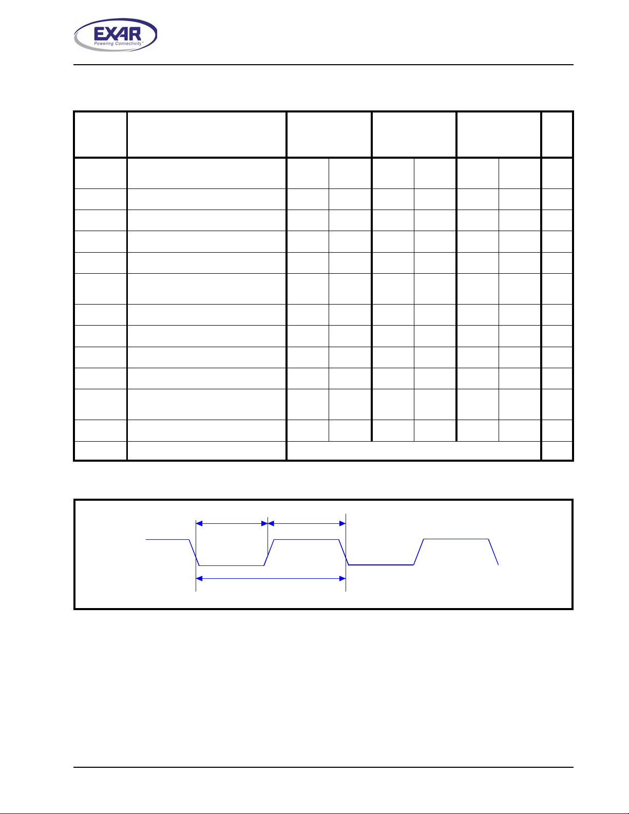
XR16M780
REV. 1.0.0
AC ELECTRICAL CHARACTERISTICS
O
TA = -40
S
TO +85OC, VCC IS 1.62 TO 3.6V, 70 PF
YMBOL
T
MOD
T
RSI
T
SSI
T
RRI
T
SI
T
INT
T
WRI
T
SSR
T
RR
Delay T o Set Interrupt From MODEM
Input
Delay To Reset Interrupt From IOR# 50 50 50 ns
Delay From Stop To Set Interrupt 1 1 1 Bclk
Delay From IOR# To Reset Interrupt 45 45 45 ns
Delay From Start To Interrupt 45 45 45 ns
Delay From Initial INT Reset To
Transmit Start
Delay From IOW# To Reset Interrupt 45 45 45 ns
Delay From Stop To Set RXRDY# 1 1 1 Bclk
Delay From IOR# To Reset RXRDY# 45 45 45 ns
P
ARAMETER
1.62V TO 3.63V HIGH PERFORMANCE UART WITH 64-BYTE FIFO
LOAD WHERE APPLICABLE
L
IMITS
1.8V ± 10%
M
IN
M
AX
50 50 50 ns
8 24 8 24 8 24 Bclk
L
IMITS
2.5V ± 10%
M
IN
M
AX
L
IMITS
3.3V ± 10%
M
IN
M
AX
U
NIT
T
T
WT
SRT
Delay From IOW# To Set TXRDY# 45 45 45 ns
Delay From Center of Start To Reset
8 8 8 Bclk
TXRDY#
T
RST
Reset Pulse Width 40 40 40 ns
Bclk Baud Clock 16X or 8X or 4X of data rate Hz
F
IGURE
16. C
LOCK TIMING
CLK
EXTERNAL
CLOCK
OSC
CLK
47
Page 48
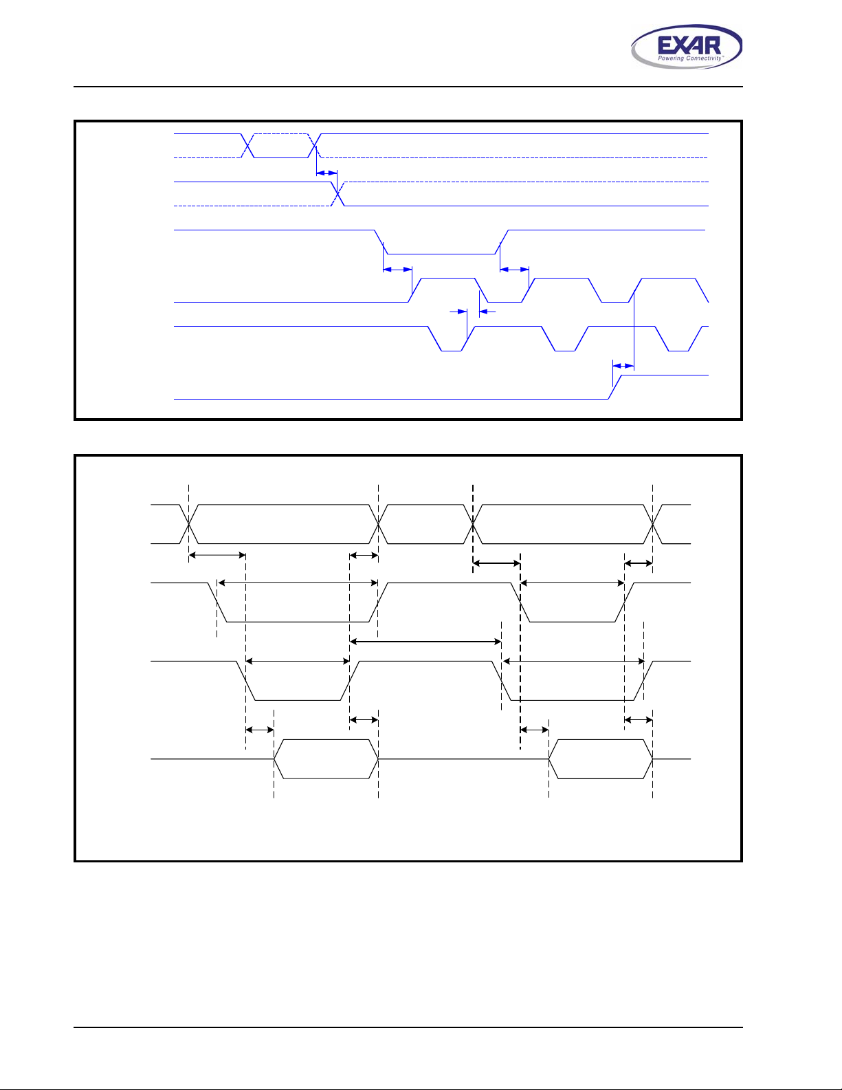
XR16M780
1.62V TO 3.63V HIGH PERFORMANCE UART WITH 64-BYTE FIFO
F
IGURE
F
IGURE
17. M
IO W #
IO W
RTS#
DTR#
CD#
CTS#
DSR#
IN T
IO R #
RI#
18. 16 M
ODEM INPUT/OUTPUT TIMING
Active
Change of state
ODE
(I
NTEL
) D
ATA BUS READ TIMING
T
WDO
Change of state
T
MOD
Change of state
Active Active
Active
T
RSI
Change of state
T
MOD
Active
A c tive A ctive
T
MOD
Change of state
REV. 1.0.0
A0-A2
CS#
IOR#
D0-D7
Valid Address Valid Address
T
AS
T
CS
T
RD
T
RDV
T
AH
T
DY
T
DD
T
AS
T
CS
T
RD
T
RDV
T
AH
T
DD
Valid Data Valid Data
RDTm
48
Page 49
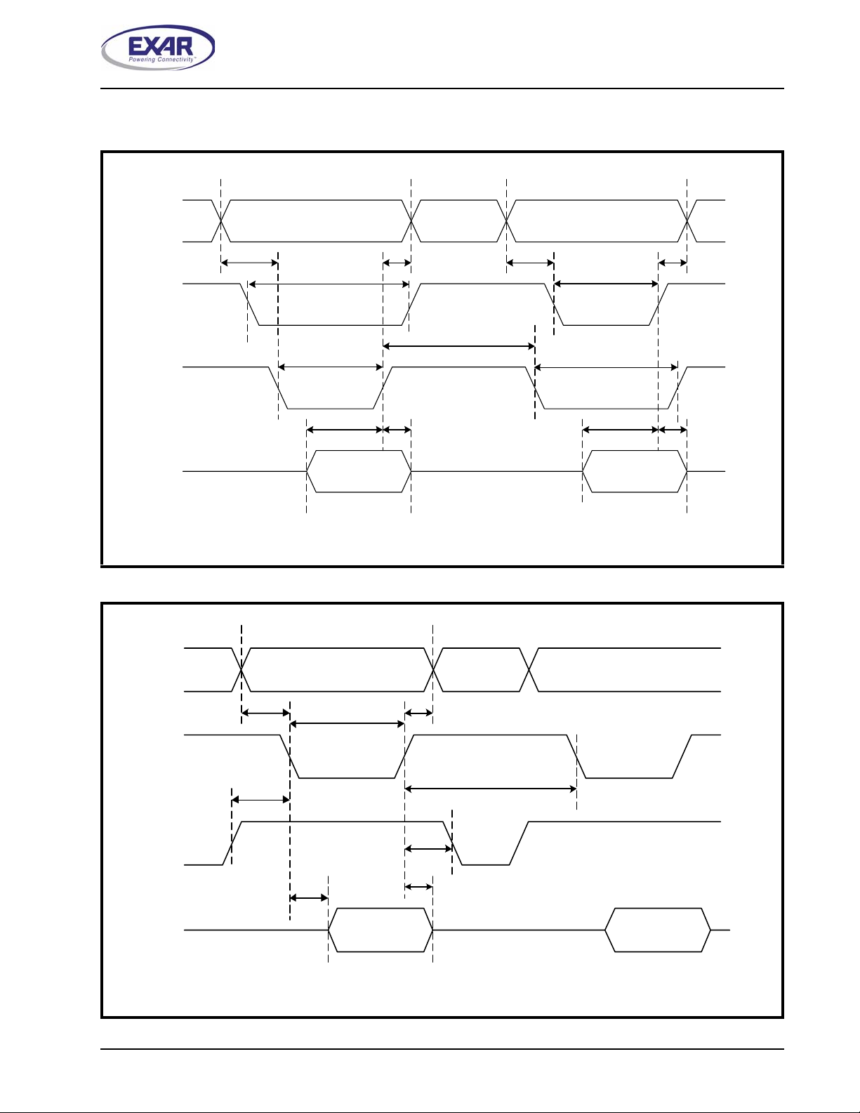
XR16M780
REV. 1.0.0
F
IGURE
A0-A2
IOW#
D0-D7
19. 16 M
CS#
ODE
(I
NTEL
T
AS
1.62V TO 3.63V HIGH PERFORMANCE UART WITH 64-BYTE FIFO
) D
ATA BUS WRITE TIMING
Valid Address Valid Address
T
T
T
CS
T
WR
T
DS
AH
T
DY
T
DH
Valid Data Valid Data
AS
T
T
CS
T
WR
T
DS
AH
T
DH
F
IGURE
20. 68 M
A0-A2
CS#
R/W#
ODE
(M
OTOROLA
T
ADS
T
RWS
RDA
T
) D
ATA BUS READ TIMING
Valid Address Valid Address
T
RWH
T
T
ADH
RDH
T
CSD
CSL
T
16Write
D0-D7
Valid Data
Va lid Data
68Read
49
Page 50
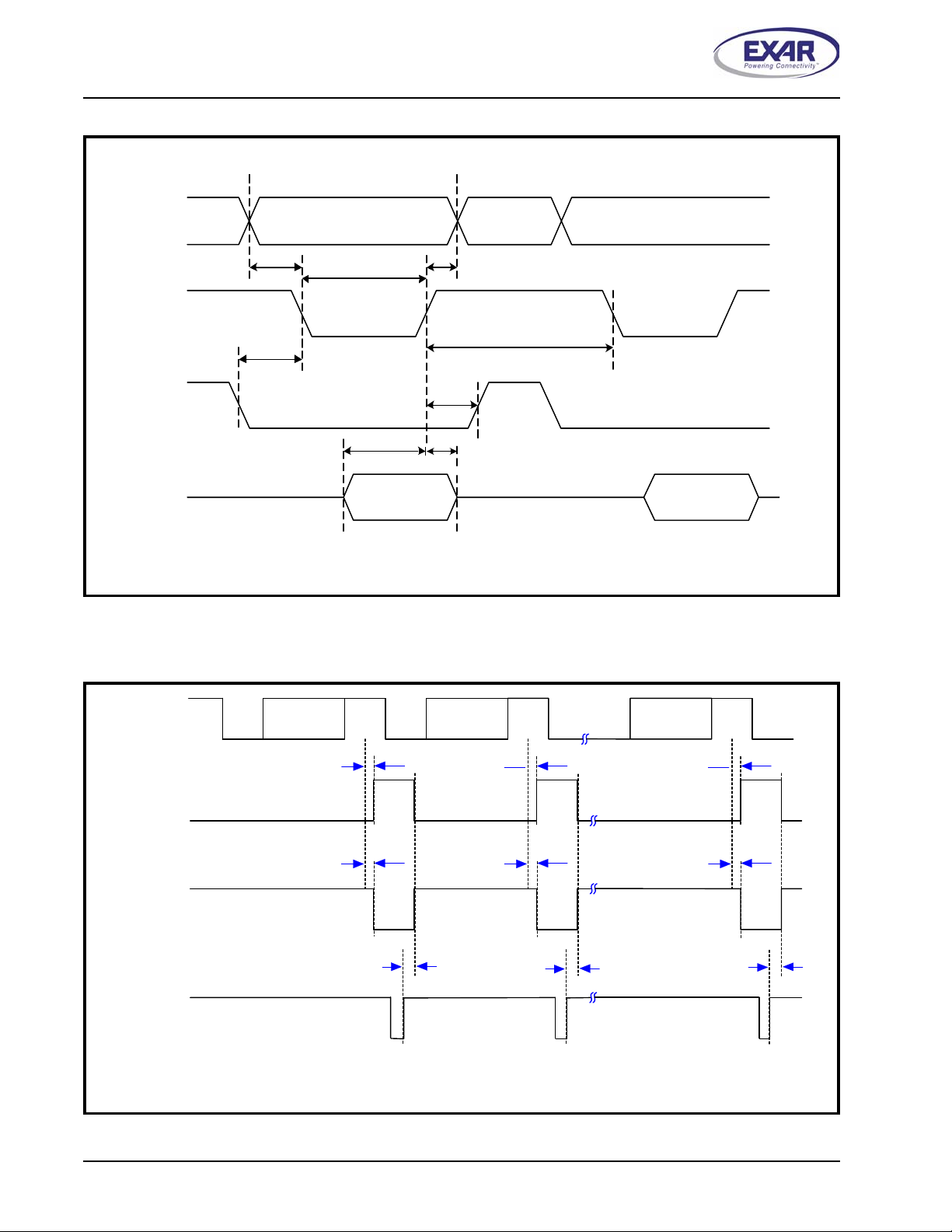
XR16M780
1.62V TO 3.63V HIGH PERFORMANCE UART WITH 64-BYTE FIFO
F
IGURE
21. 68 M
A0-A2
CS#
R/W#
D0-D7
ODE
(M
OTOROLA
T
ADS
T
RWS
) D
ATA BUS WRITE TIMING
Valid Address Valid Address
T
RWH
T
T
WDH
ADH
CSD
T
CSL
T
WDS
T
Valid Data
REV. 1.0.0
Valid Data
F
IGURE
22. R
ECEIVE READY
RX
INT
RXRDY#
IOR#
(Reading data
out of RHR)
Start
Bit
& I
NTERRUPT TIMING
D0:D7
Stop
Bit
T
T
SSR
1 Byte
in RHR
T
SSR
Active
Data
Ready
RR
[NON-FIFO M
D0:D7
ODE
T
]
T
SSR
1 Byte
in RHR
T
SSR
Active
Data
Ready
RR
D0:D7
in RHR
T
T
RR
68Write
T
SSR
1 Byte
SSR
Active
Data
Ready
50
RXNFM
Page 51
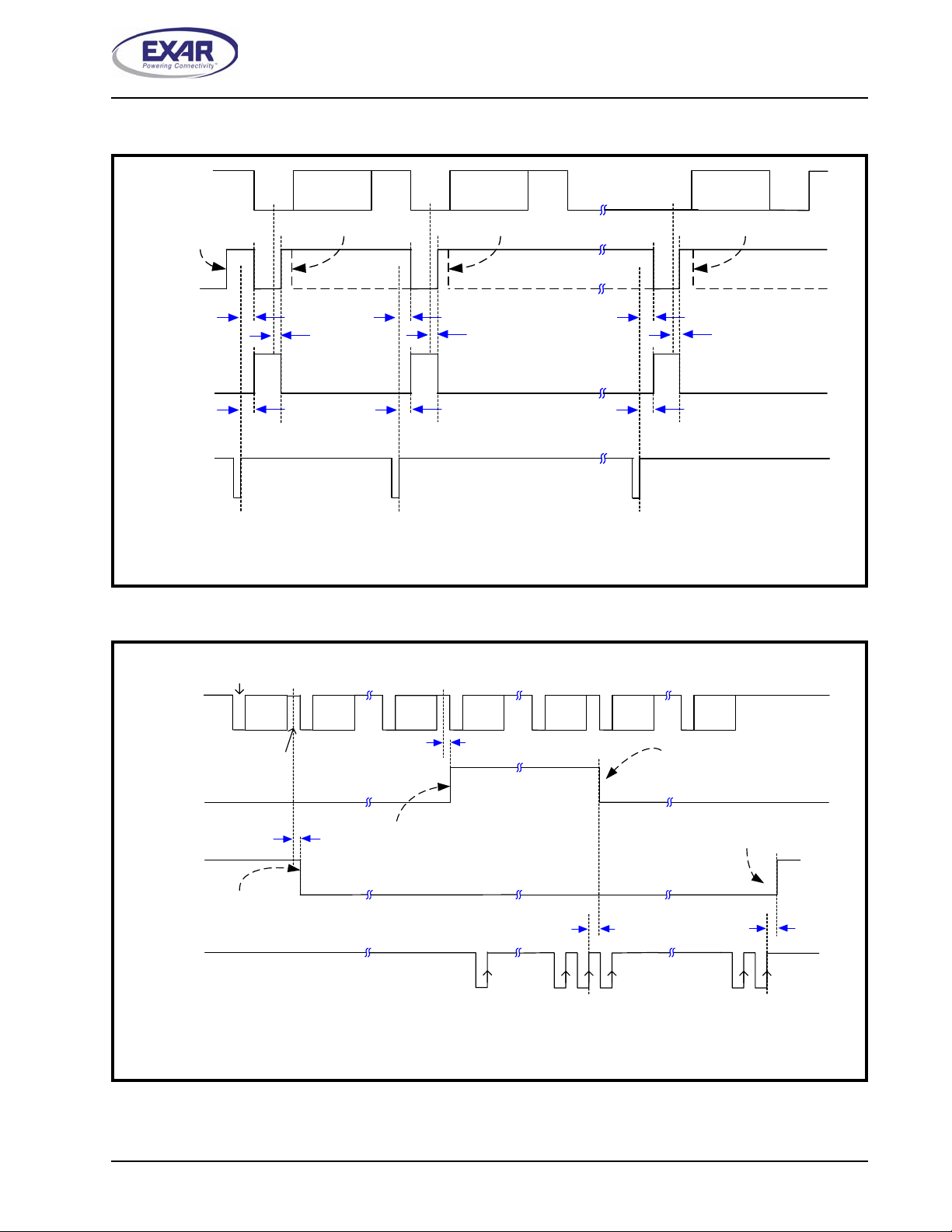
XR16M780
REV. 1.0.0
F
IGURE
TX
(Unloading)
INT*
TXRDY#
IOW#
(Loading data
into THR)
23. T
RANSMIT READY
IER[1]
enabled
T
WRI
Start
T
WT
1.62V TO 3.63V HIGH PERFORMANCE UART WITH 64-BYTE FIFO
& I
NTERRUPT TIMING
Bit
D0:D7
ISR is read ISR is readISR is read
T
SRT
Stop
Bit
T
WRI
T
WT
[NON-FIFO M
D0:D7
T
SRT
ODE
]
D0:D7
T
WRI
T
SRT
T
WT
*INT is cleared when the ISR is read or when data is loaded into the THR.
F
IGURE
24. R
ECEIVE READY
RX
INT
RXRDY#
First Byte is
Received in
IOR#
(Reading data out
of RX FIFO)
Start
Bit
S
RX FIFO
D0:D7
Stop
Bit
& I
NTERRUPT TIMING
S
D0:D7
T
T
SSR
RX FIFO fills up to RX
Trigger Level or RX Data
D0:D7
T
SSI
Timeout
[FIFO M
S
D0:D7
ODE
T
]
S
D0:D7
TXNonFIFO
S
T
D0:D7
T
S
D0:D7
T
RX FIFO drops
below RX
Trigger Level
FIFO
Empties
T
RRI
T
RR
51
RXINTDMA#
Page 52
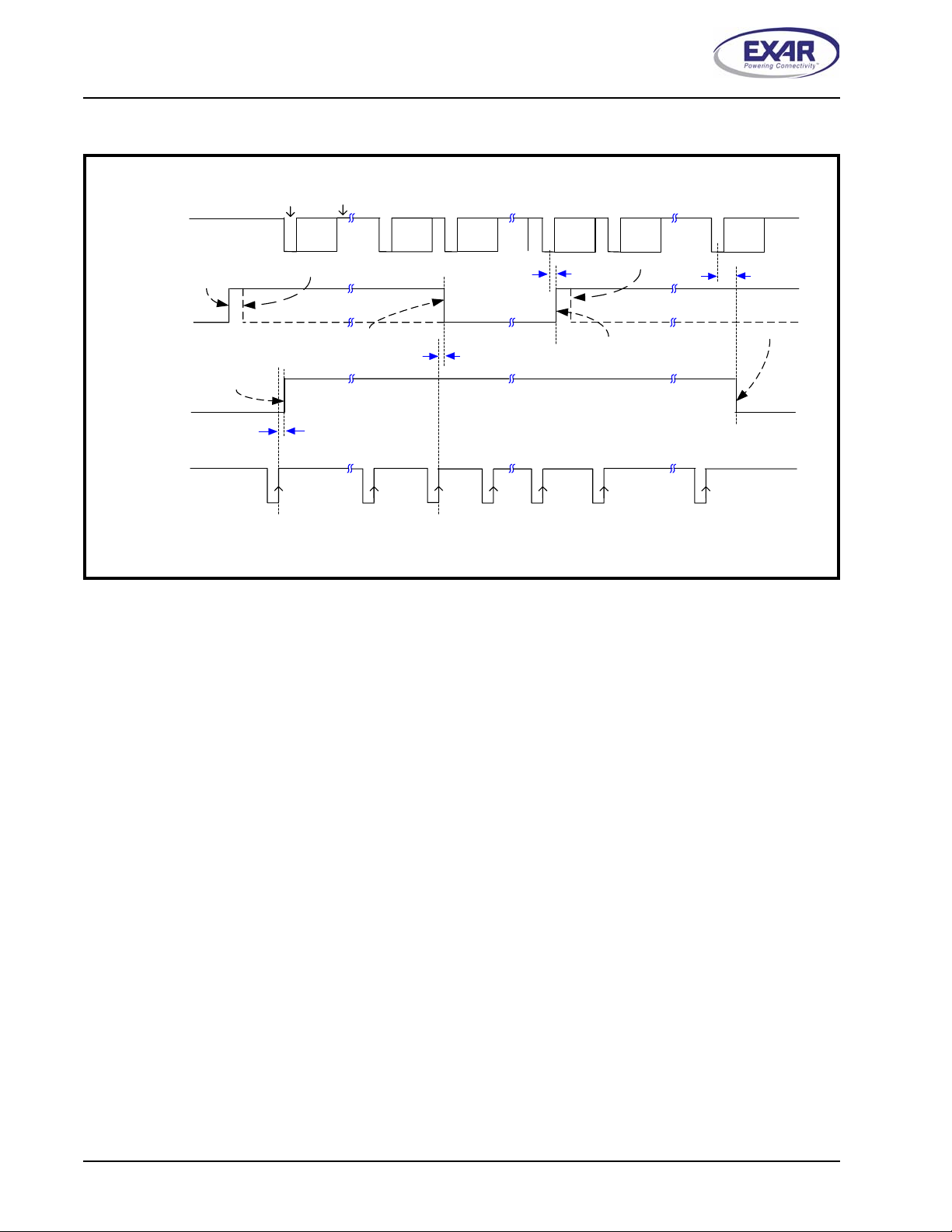
XR16M780
1.62V TO 3.63V HIGH PERFORMANCE UART WITH 64-BYTE FIFO
F
IGURE
25. T
RANSMIT READY
TX FIFO
Empty
TX
(Unloading)
IER[1]
enabled
INT*
Data in
TXRDY#
IOW#
(Loading data
into FIFO)
*INT is cleared when the ISR is read or when TX FIFO fills up to the trigger level.
TX FIFO
& I
NTERRUPT TIMING
S
D0:D7
ISR is read
TX FIFO fills up
to trigger level
T
WT
Stop
Bit
T
Start
Bit
D0:D7
[FIFO M
S
D0:D7
TS
T
WRI
ODE
]
T
S
T
T
SI
S
T
D0:D7
ISR is read
TX FIFO drops
below trigger level
D0:D7
REV. 1.0.0
Last Data Byte
Transmitted
T
S
D0:D7
TX FIFO
Empty
TXDMA#
T
T
SRT
52
Page 53
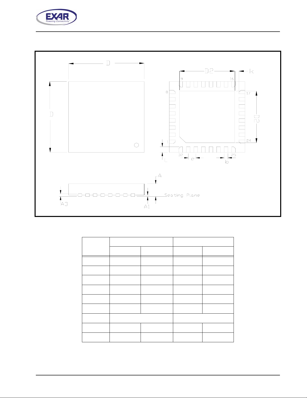
XR16M780
REV. 1.0.0
1.62V TO 3.63V HIGH PERFORMANCE UART WITH 64-BYTE FIFO
PACKAGE DIMENSIONS (32 PIN QFN - 5 X 5 X 0.9 mm)
Note: the actual center pad
is metallic and the size (D2)
is device-dependent with a
typical tolerance of 0.3mm
Note: The control dimension is in millimeter.
INCHES MILLIMETERS
SYMBOL MIN MAX MIN MAX
A 0.031 0.039 0.80 1.00
A1 0.000 0.002 0.00 0.05
A3 0.006 0.010 0.15 0.25
D 0.193 0.201 4.90 5.10
D2 0.138 0.150 3.50 3.80
b 0.007 0.012 0.18 0.30
e 0.0197 BSC 0.50 BSC
L 0.012 0.020 0.35 0.45
k 0.008 - 0.20 -
53
Page 54
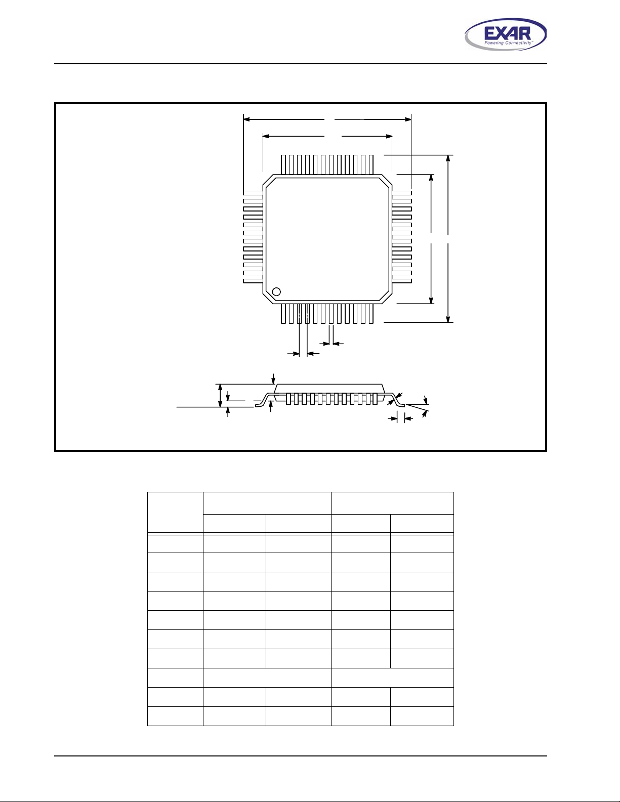
XR16M780
1.62V TO 3.63V HIGH PERFORMANCE UART WITH 64-BYTE FIFO
PACKAGE DIMENSIONS (48 PIN TQFP - 7 X 7 X 1 mm)
D
D
1
36 25
37
48
1
REV. 1.0.0
24
D
D
1
13
1
2
B
e
A
2
Seating
Plane
A
A
1
L
Note: The control dimension is the millimeter column
INCHES MILLIMETERS
SYMBOL MIN MAX MIN MAX
A 0.039 0.047 1.00 1.20
A1 0.002 0.006 0.05 0.15
A2 0.037 0.041 0.95 1.05
B 0.007 0.011 0.17 0.27
C 0.004 0.008 0.09 0.20
D 0.346 0.362 8.80 9.20
C
α
D1 0.272 0.280 6.90 7.10
e 0.020 BSC 0.50 BSC
L 0.018 0.030 0.45 0.75
a 0× 7× 0× 7×
54
Page 55
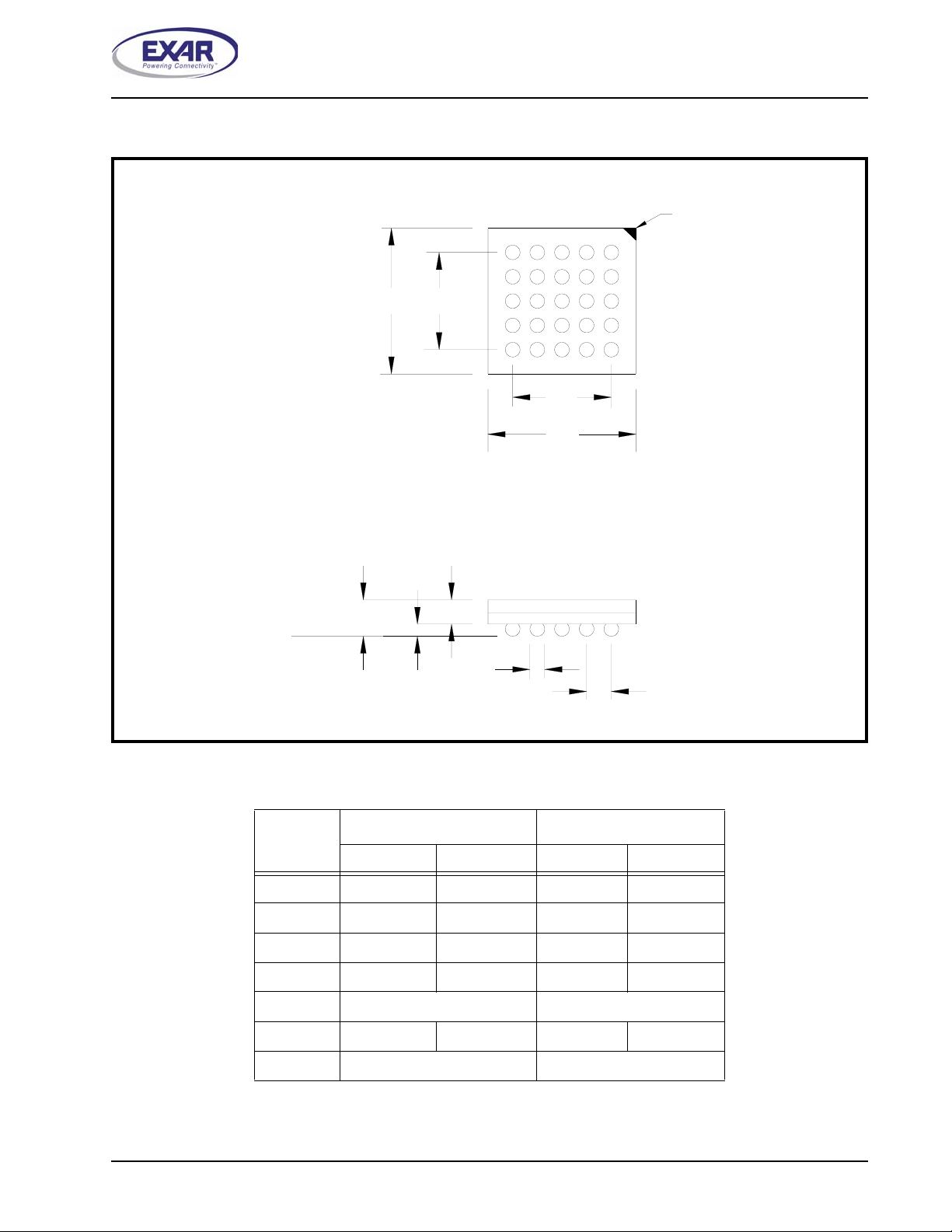
XR16M780
REV. 1.0.0
1.62V TO 3.63V HIGH PERFORMANCE UART WITH 64-BYTE FIFO
PACKAGE DIMENSIONS (25 PIN BGA - 3 X 3 X 0.8 mm)
D
D1
D1
D
(A1 corner feature is mfger option)
13245
A1 corner
A
B
C
D
E
Seating
Plane
b
A
Note: The control dimension is the millimeter column
SYMBOL MIN MAX MIN MAX
A 0.028 0.031 0.70 0.80
A1 0.005 0.007 0.13 0.19
A2 0.022 0.024 0.57 0.61
D 0.114 0.122 2.90 3.10
D1 0.079 BSC 2.00 BSC
b 0.008 0.012 0.20 0.30
e 0.020 BSC 0.50 BSC
A2
A1
INCHES MILLIMETERS
e
55
Page 56
XR16M780
1.62V TO 3.63V HIGH PERFORMANCE UART WITH 64-BYTE FIFO
REVISION HISTORY
D
ATE
September 2008 Rev 1.0.0 Final Datasheet.
R
EVISION
D
ESCRIPTION
REV. 1.0.0
NOTICE
EXAR Corporation reserves the right to make changes to the products contained in this publication in order to
improve design, performance or reliability. EXAR Corporation assumes no responsibility for the use of any
circuits described herein, conveys no lice nse under an y p atent or ot her right , and makes no rep resent atio n that
the circuits are free of patent infringement. Charts and schedules contained here in are only for illustration
purposes and may vary depending upon a user’s specific application. While the information in this publication
has been carefully checked; no responsibility, however, is assumed for inaccuracies.
EXAR Corporation does not recommend the use of any of its products in life support applications where the
failure or malfunction of the product can reasonably be expected to cause failure of the life support system or
to significantly affect its saf ety o r effectiveness. Products are not authorized for use in such a ppl icatio ns u nless
EXAR Corporation receives, in writing, assurances to its satisfaction that: (a) the risk of injury or damage has
been minimized; (b) the user assumes all such risks; (c) potential liability of EXAR Corporation is adequately
protected under the circumstances.
Copyright 2008 EXAR Corporation
Datasheet September 2008.
Send your UART technical inquiry with technical details to hotline: [email protected].
Reproduction, in part or whole, without the prior written consent of EXAR Corporation is prohibited.
56
Page 57

XR16M780
REV. 1.0.0
1.62V TO 3.63V HIGH PERFORMANCE UART WITH 64-BYTE FIFO
GENERAL DESCRIPTION................................................................................................ 1
F
EATURES
A
PPLICATIONS
F
F
F
ORDERING INFORMATION
.................................................................................................................................................... 1
.............................................................................................................................................. 1
IGURE
1. XR16M780 B
IGURE
2. PIN OUT A
IGURE
3. PIN OUT A
LOCK DIAGRAM
SSIGNMENT FOR
SSIGNMENT FOR
.......................................................................................................................................... 1
32-
PIN
QFN
AND
48-
PIN
25-
PIN
BGA P
ACKAGE
TQFP P
........................................................................................................... 3
ACKAGES IN
16
AND
68 M
ODE
............................................. 2
............................................................................................................................... 3
PIN DESCRIPTIONS ........................................................................................................ 4
1.0 PRODUCT DESCRIPTION ..................................................................................................................... . 7
2.0 FUNCTIONAL DESCRIPTIONS ................ ... ... ... .... ... ... ... .... ... ... ... .... ... ... ... ... .... ... ... ... .... ... ... ... ... ....... ... .... 8
2.1 CPU INTERFACE ................................................................................................................................................ 8
F
IGURE
4. XR16M780 T
2.2 SERIAL INTERFACE........................................................................................................................................... 9
F
IGURE
5. XR16M780 T
F
IGURE
6. XR16M780 T
2.3 DEVICE RESET................................................................................................................................................. 11
2.4 INTERNAL REGISTERS.................................................................................................................................... 11
2.5 INT OUPUT........................................................................................................................................................ 11
T
ABLE
1: INT PIN O
T
ABLE
2: INT PIN O
2.6 CRYSTAL OSCILLATOR OR EXTERNAL CLOCK INPUT.............................................................................. 12
F
IGURE
7. T
YPICAL CRYSTAL CONNECTIONS
2.7 PROGRAMMABLE BAUD RATE GENERATOR WITH FRACTIONAL DIVISOR........................................... 13
2.7.1 INDEPENDENT TX/RX BRG......................................................................................................................................... 13
F
IGURE
8. B
T
ABLE
AUD RATE GENERATOR
3: T
YPICAL DATA RATES WITH A
2.8 TRANSMITTER.................................................................................................................................................. 15
2.8.1 TRANSMIT HOLDING REGISTER (THR) - WRITE ONLY........................................................................................... 15
2.8.2 TRANSMITTER OPERATION IN NON-FIFO MODE. ................................................................................................... 15
F
IGURE
9. T
RANSMITTER OPERATION IN NON
2.8.3 TRANSMITTER OPERATION IN FIFO MODE ............................................................................................................. 16
F
IGURE
10. T
RANSMITTER OPERATION IN
2.9 RECEIVER......................................................................................................................................................... 16
2.9.1 RECEIVE HOLDING REGISTER (RHR) - READ-ONLY .............................................................................................. 16
F
IGURE
11. R
F
IGURE
ECEIVER OPERATION IN NON
12. R
ECEIVER OPERATION IN
2.10 AUTO RTS (HARDWARE) FLOW CONTROL................................................................................................ 18
2.11 AUTO RTS HYSTERESIS ............................................................................................................................... 18
T
ABLE
4: A
UTO
RTS (H
2.12 AUTO CTS FLOW CONTROL......................................................................................................................... 18
F
IGURE
13. A
UTO
2.13 AUTO XON/XOFF (SOFTWARE) FLOW CONTROL...................................................................................... 20
T
ABLE
5: A
UTO XON/XOFF
2.14 SPECIAL CHARACTER DETECT.................................................................................................................. 20
2.15 NORMAL MULTIDROP MODE........................................................................................................................ 20
2.15.1 AUTO ADDRESS DETECTION .................................................................................................................................. 21
2.16 INFRARED MODE........................................................................................................................................... 21
F
IGURE
14. I
NFRARED TRANSMIT DATA ENCODING AND RECEIVE DATA DECODING
2.17 SLEEP MODE WITH AUTO WAKE-UP AND POWER-SAVE FEATURE...................................................... 22
2.17.1 SLEEP MODE ............................................................................................................................................................. 22
2.17.2 POWER-SAVE FEATURE .......................................................................................................................................... 23
2.17.3 WAKE-UP INTERRUPT .............................................................................................................................................. 23
2.18 INTERNAL LOOPBACK................................................................................................................................. 24
F
IGURE
15. I
NTERNAL LOOPBACK
3.0 UART INTERNAL REGISTERS............................................................................................................. 25
T
ABLE
6: UART INTERNAL REGISTERS .................................................................................................................................. 25
T
ABLE
7: INTERNAL REGISTERS DESCRIPTION. S
4.0 INTERNAL REGISTER DESCRIPTIONS.............................................................................................. 27
4.1 RECEIVE HOLDING REGISTER (RHR) - READ- ONLY.................................................................................. 27
4.2 TRANSMIT HOLDING REGISTER (THR) - WRITE-ONLY............................................................................... 27
4.3 INTERRUPT ENABLE REGISTER (IER) - READ/WRITE ................................................................................ 28
4.3.1 IER VERSUS RECEIVE FIFO INTERRUPT MODE OPERATION ............................................................................... 28
YPICAL INTEL/MOTOROLA DATA BUS INTERCONNECTIONS
YPICAL SERIAL INTERFACE CONNECTIONS
YPICAL SERIAL INTERFACE CONNECTIONS
PERATION FOR TRANSMITTER
PERATION FOR RECEIVER
........................................................................................................................... 11
................................................................................................................................ 11
.................................................................................................................................. 12
............................................................................................................................................... 14
RTS
ARDWARE
AND
CTS F
(S
OFTWARE
24 MHZ
FIFO
) F
LOW CONTROL
LOW CONTROL OPERATION
CRYSTAL OR EXTERNAL CLOCK AT
-FIFO M
ODE
.............................................................................................................. 15
FIFO
AND FLOW CONTROL MODE
-FIFO M
ODE
AND AUTO
.................................................................................................................. 17
RTS F
........................................................................................................................ 18
) F
LOW CONTROL
............................................................................................................... 20
LOW CONTROL MODE
....................................................................................................... 19
................................................................................................................................................... 24
HADED BITS ARE ENABLED WHEN
............................................................................ 8
................................................................................................... 9
................................................................................................. 10
16X S
AMPLING
................................................... 14
................................................................................... 16
....................................................................... 17
.......................................................................... 22
EFR BIT-4=1 ......................................... 26
I
Page 58

XR16M780
1.62V TO 3.63V HIGH PERFORMANCE UART WITH 64-BYTE FIFO
REV. 1.0.0
4.3.2 IER VERSUS RECEIVE/TRANSMIT FIFO POLLED MODE OPERATION.................................................................. 28
4.4 INTERRUPT STATUS REGISTER (ISR) - READ-ONLY .................................................................................. 29
4.4.1 INTERRUPT GENERATION: ........................................................................................................................................ 29
4.4.2 INTERRUPT CLEARING: ............................................................................................................................................. 30
T
ABLE
8: I
NTERRUPT SOURCE AND PRIORITY LEVEL
....................................................................................................................... 30
4.5 FIFO CONTROL REGISTER (FCR) - WRITE-ONLY......................................................................................... 31
T
ABLE
9: T
RANSMIT AND RECEIVE
FIFO T
RIGGER TABLE AND LEVEL SELECTION
............................................................................ 32
4.6 LINE CONTROL REGISTER (LCR) - READ/WRITE......................................................................................... 32
T
ABLE
10: P
ARITY SELECTION
........................................................................................................................................................ 33
4.7 MODEM CONTROL REGISTER (MCR) OR GENERAL PURPOSE OUTPUTS CONTROL - READ/WRITE.. 34
T
ABLE
11: INT O
UTPUT MODES
..................................................................................................................................................... 34
4.8 LINE STATUS REGISTER (LSR) - READ ONLY.............................................................................................. 35
4.9 MODEM STATUS REGISTER (MSR) - READ ONLY....................................................................................... 36
4.10 MODEM STATUS REGISTER (MSR) - WRITE ONLY.................................................................................... 37
4.11 SCRATCH PAD REGISTER (SPR) - READ/WRITE ....................................................................................... 37
4.12 ENHANCED MODE SELECT REGISTER (EMSR) - WRITE-ONLY ............................................................... 38
T
ABLE
12: S
T
ABLE
CRATCHPAD SWAP SELECTION
13: A
UTO
RTS H
YSTERESIS
.................................................................................................................................... 38
................................................................................................................................................ 39
4.13 BAUD RATE GENERATOR REGISTERS (DLL, DLM AND DLD) - READ/WRITE ....................................... 39
T
ABLE
14: S
T
ABLE
AMPLING RATE SELECT
15: BRG S
ELECT
................................................................................................................................................................ 40
............................................................................................................................................... 40
4.14 TRIGGER LEVEL REGISTER (TRG) - WRITE-ONLY.................................................................................... 40
4.15 RX/TX FIFO LEVEL COUNT REGISTER (FC) - READ-ONLY ....................................................................... 40
4.16 FEATURE CONTROL REGISTER (FCTR) - READ/WRITE............................................................................ 41
T
ABLE
16: T
RIGGER TABLE SELECT
................................................................................................................................................ 41
4.17 ENHANCED FEATURE REGISTER (EFR) - READ/WRITE ........................................................................... 41
T
ABLE
17: S
OFTWARE FLOW CONTROL FUNCTIONS
........................................................................................................................ 42
4.18 SOFTWARE FLOW CONTROL REGISTERS (XOFF1, XOFF2, XON1, XON2) - READ/WRITE................... 43
T
ABLE
18: UART RESET CONDITIONS ...................................................................................................................................... 44
ABSOLUTE MAXIMUM RATINGS.................................................................................. 45
TYPICAL PACKAGE THERMAL RESISTANCE DATA (MARGIN OF ERROR: ± 15%) 45
ELECTRICAL CHARACTERISTICS............................................................................... 45
DC E
LECTRICAL CHARACTERISTICS
AC E
LECTRICAL CHARACTERISTICS
TA = -40O TO +85OC, VCC IS 1.62 TO 3.6V, 70 PF
F
IGURE
16. C
F
IGURE
F
IGURE
F
IGURE
F
IGURE
F
IGURE
F
IGURE
F
IGURE
F
IGURE
F
IGURE
LOCK TIMING
17. M
ODEM INPUT/OUTPUT TIMING
18. 16 M
19. 16 M
20. 68 M
22. R
21. 68 M
23. T
24. R
25. T
ODE
ODE
ODE
ECEIVE READY
ODE
RANSMIT READY
ECEIVE READY
RANSMIT READY
............................................................................................................................................................. 47
(I
NTEL
) D
(I
NTEL
) D
(M
OTOROLA
& I
(M
OTOROLA
& I
& I
& I
............................................................................................................. 45
............................................................................................................. 46
.................................................................................................................................... 48
ATA BUS READ TIMING
ATA BUS WRITE TIMING
) D
ATA BUS READ TIMING
NTERRUPT TIMING
) D
ATA BUS WRITE TIMING
NTERRUPT TIMING
NTERRUPT TIMING
NTERRUPT TIMING
[NON-FIFO M
[NON-FIFO M
[FIFO M
[FIFO M
LOAD WHERE APPLICABLE
................................................................................................................... 48
.................................................................................................................. 49
.......................................................................................................... 49
ODE
]............................................................................................ 50
......................................................................................................... 50
ODE
].......................................................................................... 51
ODE
].................................................................................................... 51
ODE
].................................................................................................. 52
............................................. 46
PACKAGE DIMENSIONS (32 PIN QFN - 5 X 5 X 0.9 mm).............................................. 53
PACKAGE DIMENSIONS (48 PIN TQFP - 7 X 7 X 1 mm)............................................... 54
PACKAGE DIMENSIONS (25 PIN BGA - 3 X 3 X 0.8 mm).............................................. 55
R
EVISION HISTORY
...................................................................................................................................... 56
II
 Loading...