

Page 1
查询XR-T56L85供应商
...the analog plus company
FEA TURES10
Low Power (Typical 14mA)
Single +5V Supply
Up to 2.048 Mbps Operation in Both TX and RX
Directions
Receiver Input can be:
– Balanced Transformer Coupled
– Capacitively (Twisted Pair)
– Single Coaxial Capacitive Coupling
GENERAL DESCRIPTION
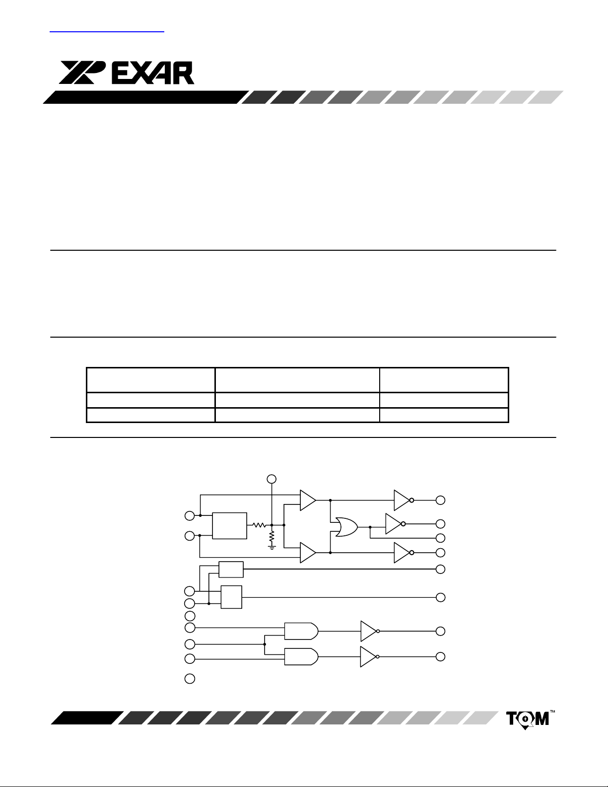
The XR-T56L85 is a PCM line interface chip. It consists of
both transmit and receive circuitry in a DIL 18 pin
package. The maximum bit rate the chip can handle is
2.048 Mbps and the signal level to the received can be
XR-T56L85
Low Power
TM
APPLICATIONS
T1 and CEPT Interfaces
CPI
DMI
attenuated by 10dB of cable loss at half the bit rate. T otal
current consumption is between 12-16mA at +5V.
PCM Line Interface
June 1997-3
ORDERING INFORMA TION
Part No. Package
XR-T56L85N 18 Lead 300 Mil CDIP -40°C to +85°C
XR-T56L85D 18 Lead 300 Mil JEDEC SOIC -40°C to +85°C
BLOCK DIAGRAM
RXDATA+
RXDATA-
RXV
RXGND
TXV
TPOS
TCLK
TNEG
CC
CC
Operating
T emperature Range
Positive
PDC
Threshold
1
Comparator
+
–
2
3
9
7
18
17
16
12
Peak
Detector
Bias
Bias
Negative
Threshold
Comparator
–
+
TTL Buffer
TTL Buffer
TTL Buffer
TTL Buffer
TTL Buffer
RPOS
11
8
RCLK
4
TE
RNEG
10
TANK BIAS
6
5
BIAS
15
TXDATA+
13
TXDATA-
Rev. 2.01
1992
TXGND
14
Figure 1. Block Diagram
EXAR Corporation, 48720 Kato Road, Fremont, CA 94538 (510) 668-7000 FAX (510) 668-7017
1
Page 2
XR-T56L85
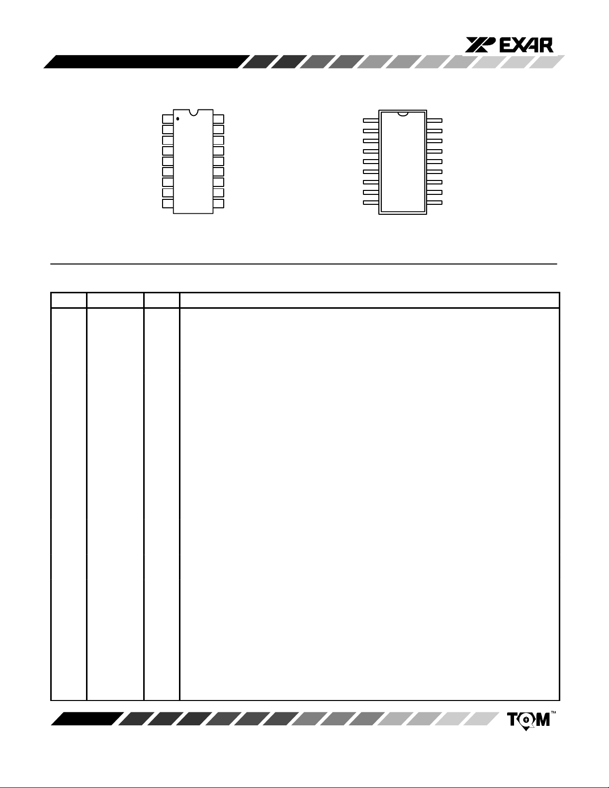
PIN CONFIGURATION
PDC
RXDATA+
RXDATA-
TE
BIAS
TANK BIAS
RXGND
RCLK
CC
18 Lead CDIP (0.300”)
1
2
3
4
5
6
7
8
9
18
17
16
15
14
13
12
11
10
TXV
CC
TPOS
TCLK
TXDATA+
TXGND
TXDATATNEG
RPOS
RNEGRXV
PDC
RXDATA+
RXDATA-
TE
BIAS
TANK BIAS
RXGND
RCLK
CC
181
2
17
3
16
4
15
5
14
6
13
7
12
11
8
109
18 Lead SOIC (Jedec, 0.300”)
TXV
CC
TPOS
TCLK
TXDATA+
TXGND
TXDATATNEG
RPOS
RNEGRXV
PIN DESCRIPTION
Pin # Symbol Type Description
1 PDC Peak Detector Capacitor. This pin should be connected to a 0.1µF capacitor
2 RXDATA+ I Receive Analog Input Positive. The AMI signal received from the line is applied at this and
the RX DA TA(-) pin. Data and clock from the signal applied at these two pins recovered and
output on the RPOS, RNEG, and RCLK pins, respectively.
3 RXDATA- I Receive Analog Input Negative. See the description for RX DA TA(+).
4 TE O LC Tank Excitation Output. This output connects to one side of the tank circuitry.
5 BIAS O Bias. This pin should be tied to ground through a 0.1µF capacitor.
6 TANK BIAS T ank Reference. The tank circuitry is biased via this output.
7 RXGND Receiver Ground. To minimize ground interference a separate pin is used to ground the re-
ceiver section.
8 RCLK O Recovered Receive Clock. Recovered clock signal from the AMI signal received at the RX
DATA(+) and RX DATA(-) pins. This signal is output to the terminal equipment.
9 RXV
CC
10 RNEG O Receive Negative Data Output. A signal at this pin corresponds to the receipt of a negative
11 RPOS O Receive Positive Data Output. A signal at this pin corresponds to the receipt of a positive
12 TNEG I Transmit Negative Data Input. TTL input for a negative polarity pulse (the negative portion
13 TXDATA- O Transmit Negative Data Output. This pin, along with the TX DATA(+) pin, forms a differential
14 TXGND Transmit Ground.
15 TXDATA+ O Transmit Positive Data Output. Please see description for TX DATA(-).
16 TCLK I Transmit Clock. TPOS and TNEG are sampled on the rising edge of TCLK.
17 TPOS I Transmit Positive Data Input. TTL input for a positive polarity pulse (the positive portion of
18 TXVcc Transmit Supply Voltage. 5V supply voltage to the transmit section.
Receive Supply V oltage. 5V supply voltage for the Receive Section.
pulse on the RX DA TA(+)/RX DATA(-) pins. This TTL compatible signal is output to the
terminal equipment.
pulse on the RX DA TA(+)/RX DATA pins. This TTL compatible signal is outputed to the
terminal equipment.
of the AMI pulse train) to be transmitted to the line via the TX DA TA(+) and TX DATA pins.
driver output, this is used to drive AMI data down the line via a transformer. Note: This is an
open-collector output.
the AMI pulse train) to be transmitted to the line via the TX DA TA(+) and TX DATA(-) pins.
Rev. 2.01
2
Page 3
XR-T56L85
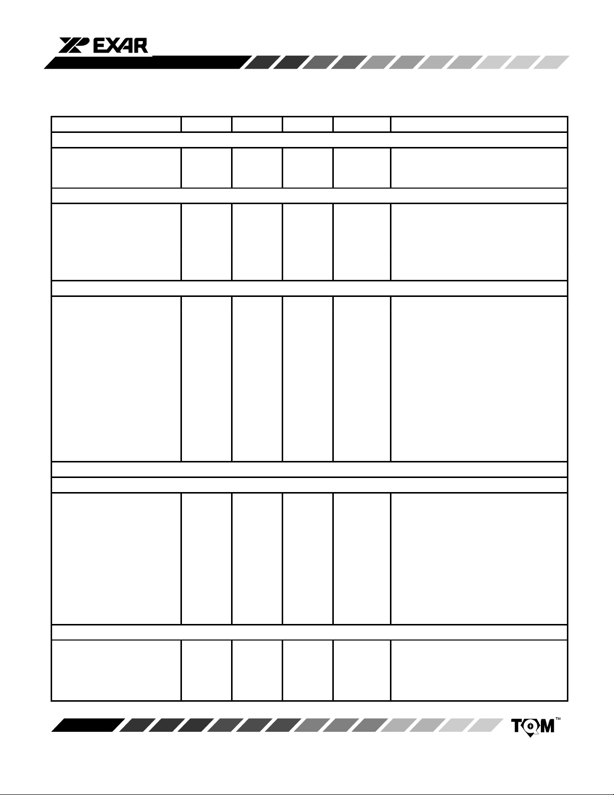
ELECTRICAL CHARACTERISTICS
Test Conditions: V
Parameters Min. Typ. Max. Unit Conditions
DC Electrical Characteristics
Supply Voltage 4.75 5 5.25 V
Supply Current 14 16 mA Total Current to Pin 9 & Pin 18 (Transmit-
Receiver Section
Tank Drive Current 300 500 700 µA Measured at Pin 4, VCC= 5V
Clock Output Low 0.3 0.6 V Measured at Pin 8, I
Clock Output High 3.0 3.6 V Measured at Pin 8, I
Data Output Low 0.3 0.6 V Measured at Pin 10 & 11, IOL =1.6mA
Data Output High 3.0 3.6 V Measured at Pin 10 & 11, IOH =400µA
Transmitter Section
Driver Output Low 0.6 0.9 1.2 V Measured at Pin 13 & 15, IOL =-40mA
Output Leakage Current 100 µA Measured in Off State
Input High Voltage 2.2 V Measured at Pin 12, 16 & 17
Input Low Voltage 0.8 V Measured at Pin 12, 16 & 17
Input Low Current -1.6 mA Measured at Pin 12, 16 & 17
Input High Current 40 µA Measured at Pin 12, 16 & 17
Output Low Current -30 mA Measured at Pin 13 & 15
AC Electrical Characteristices
Receiver Section
Input Level 6 6.6 Vpp Measured Between Pin 2 & 3
Loss Input Signal Alarm Level 0.6 Vpp Measured Between Pin 2 & 3
Input Impedance at 2.048MHz 2.5 kΩ Measured Between Pin 2 & 3
Clock Duty Cycle 35 50 65 % Measured at Pin 8 at 2.0V DC Level
Clock Rise & Fall Time 20 40 ns Measured at Pin 8, CL = 15pF
Data Pulse Width 35 50 75 % of
Transmitter Section
Pulse Width at 2.048MHz 234 244 264 ns Measured at Pin 13 & 15
Output Rise Time 12 25 ns
Output Fall Time 12 25 ns
Output Fall Imbalance 2.5 ns At 50% Output Level
= 5V5%, T
CC
= -40°C to +85°C, Unless Otherwise Specified
A
ter Outputs Open and All Ones Pattern)
Output Pull-up to +20V
= -40mA, VOL = 1.0V
I
OL
Output Off
Input Low Voltage = 0.4V
Input Low Voltage = 0.4V
= 1.0V
V
OL
Alarm on Pull Data/Clock Output High
With Sinewave Input
Measured at Pin 10 & 1 1
clock
period
At 1V DC Level, Cable Loss = dB
Figure 3
Figure 3
= 1.6mA
OL
=400µA
OH
Figure 3
Rev. 2.01
3
Page 4

XR-T56L85
ABSOLUTE MAXIMUM RATINGS
Supply Voltage +20V. . . . . . . . . . . . . . . . . . . . . . . . . . . . Storage Temperature -65°C to 150°C. . . . . . . . . . . . . .
SYSTEM DESCRIPTION
The Receiver
The incoming bipolar PCM signal, which is attenuated
and distorted by the cable is applied to the receiver input,
consisting of the RX DA TA(+) and RX DA T A(-) pins, either
through a balanced transformer, a balanced capacitively
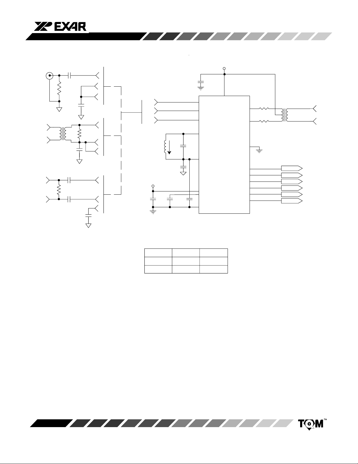
coupled terminal or a single-ended coaxial cable (see
Figure 5
DC reference for the positive and negative threshold
comparator (to extract the positive and negative data
pulses). Information on the positive and negative data
pulses is outputed as TTL compatible signals at pins
RPOS and RNEG, respectively. More specifically, an
output signal present at the RPOS pin indicates that a
positive pulse was received at the RX DATA(+)/RX
DATA(-) pins, from the incoming bipolar data stream.
Likewise an output signal present at the RNEG pin
indicates that a negative pulse was received at the RX
DATA(+)/RX DATA(-) pins. This conversion from the
bipolar signal to TTL compatible signals allows for digital
processing of the clock and data signals by the terminal
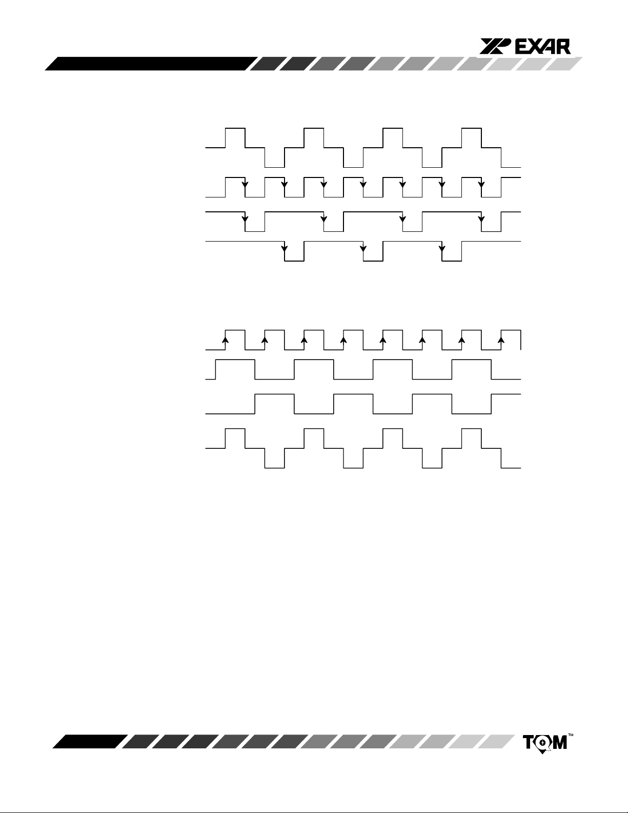
equipment. An example of the waveforms of the TTL
compatible recovered clock and data as output by the
receiver portion of the chip is presented in
Figure 3
). A peak detector following the input generates a
Figure 2
and
Figure 5
. A tank circuit tuned to the
appropriate frequency is added externally to provide the
appropriate frequency-selective filtering of the received
clock signal.
The Transmitter
The transmitter portion of the chip receives TTL
compatible signals and transmits a corresponding bipolar
data stream down the line (See
TNEG are TTL compatible signals that dictate the polarity
of the pulse to be generated and transmitted on the output
bipolar data stream. Both TPOS and TNEG inputs are
sampled by the rising edge of the transmit clock, TCLK.
The TX DATA(+) and TX DATA(-) pins form a differential
driver output, this is used to drive AMI data down the line
via a transformer. The TX DATA(+) and TX DAT A(-) pins
are open-collector outputs.
When a logic “high” signal is applied to the TPOS pin, a
positive pulse (the positive portion of the bipolar data
stream) will be transmitted to the line via the TX DA T A(+)
O/P and TX DATA(-) O/P pins. Likewise, when a logic
“high” signal is applied to the TNEG pin, a negative pulse
will be transmitted to the line via the TX DA TA(+) and TX
DATA(-) pins. An illustration of the key waveforms
involved in this TTL to AMI conversion process, in the
,
Transmitter portion of the chip is presented in
Figure 5
). TPOS and
Figure 4
.
Rev. 2.01
4
Page 5
VCC=5V
XR-T56L85
2.048Mbps
Pulse
Generator
Input
Pin 9 &18
XR-T56L85
Pin 12, 16, 17
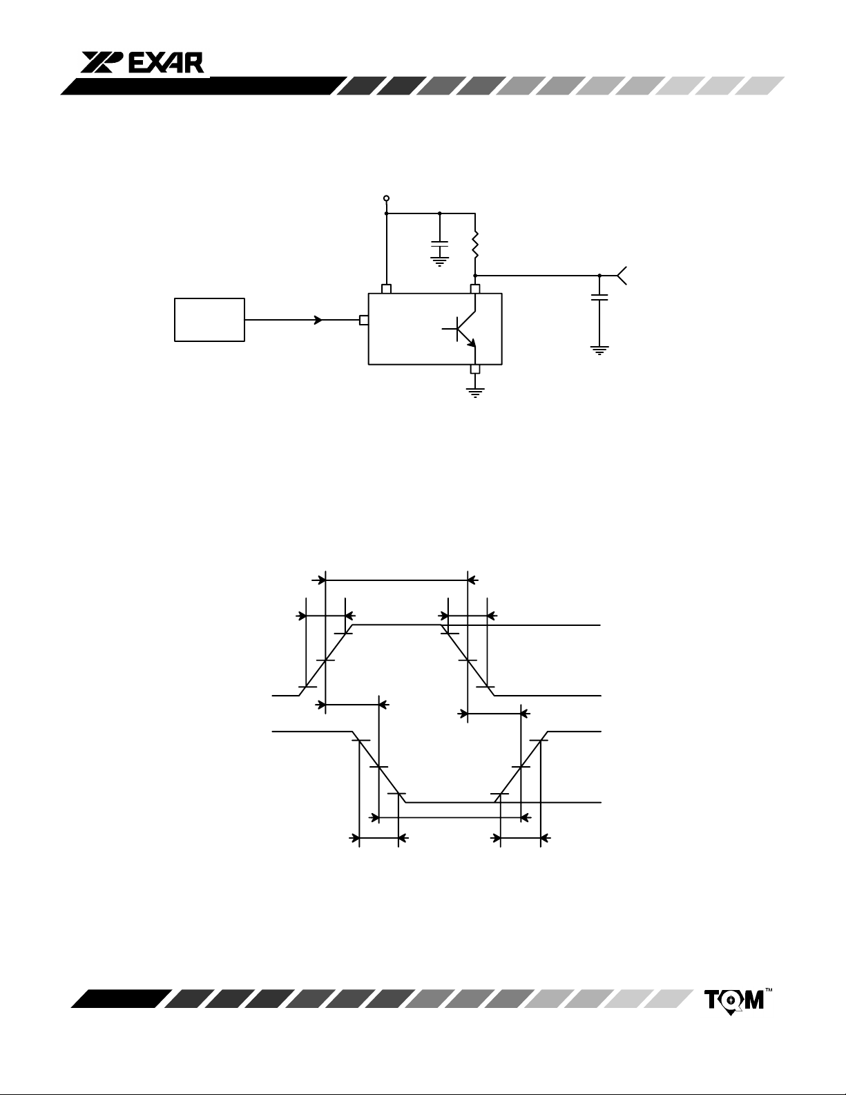
Figure 2.
244ns
90%
0.1µF
90%
100
Pin 13 & 15
Pin 7 &14
0V
<5ns<5ns
Output
CL=15pF
0V
3V
Rev. 2.01
Input Pulse
from Generator
Output from Pin 13
or Pin 15
10%
Fall Time
1.5V
1.5V
15ns Typ.
Pulse Width
Figure 3.
5
10%
0V
15ns Typ.
+5V
Vol
Rise Time
Page 6
XR-T56L85
RXDATA+
RCLK Output At Pin 8
RPOS Output At Pin 11
RNEG Output At Pin 10
TCLK Clock To Pin 16
TPOS To Pin 17
TNEG To Pin 12
Bipolar Signal At
Transformer Output
Figure 4. Receiver Timing Diagram With 1-1-1-1-1-1 Pattern
Rev. 2.01
6
Page 7
RCACON
0.1µF
75
0.1µF
120
T1
120
1:1
0.1µF
0.1µF
0.1µF
0.1µF
TIP
RING
TIP
RING 3
XR-T56L85
V
CC
2
3
5
2
3
5
2
5
0.1µF
2
3
5
4.7µF
V
CC
0.1µF
0.1µF
2
RXDATA+
3
RXDATA-
5
BIAS
4
T.E.
LC
6
TANK BIAS
9
RV
1
PDC
0.1µF
7
RGND
U1
56L85TA
V
CC
XR-T56L85
CC
18
TXDATA+
TXDATA-
TGND
TCLK
TPOS
TNEG
RPOS
RNEG
RCLK
15
56
13
56
14
16
17
12
11
10
8
T2
PE65415
1:1:1
TCLK
TPOS
TNEG
RPOS
RNEG
RCLK
TIP
RING
L=Tank Coil AIE 415–0804 (1.544 and 2.048 Mbs)
Device 1.544Mbs 2.048Mbs
L
C
60µH
175pF
60µH
100pF
Figure 5. Application Circuit for XR-T56L85
Rev. 2.01
7
Page 8
XR-T56L85
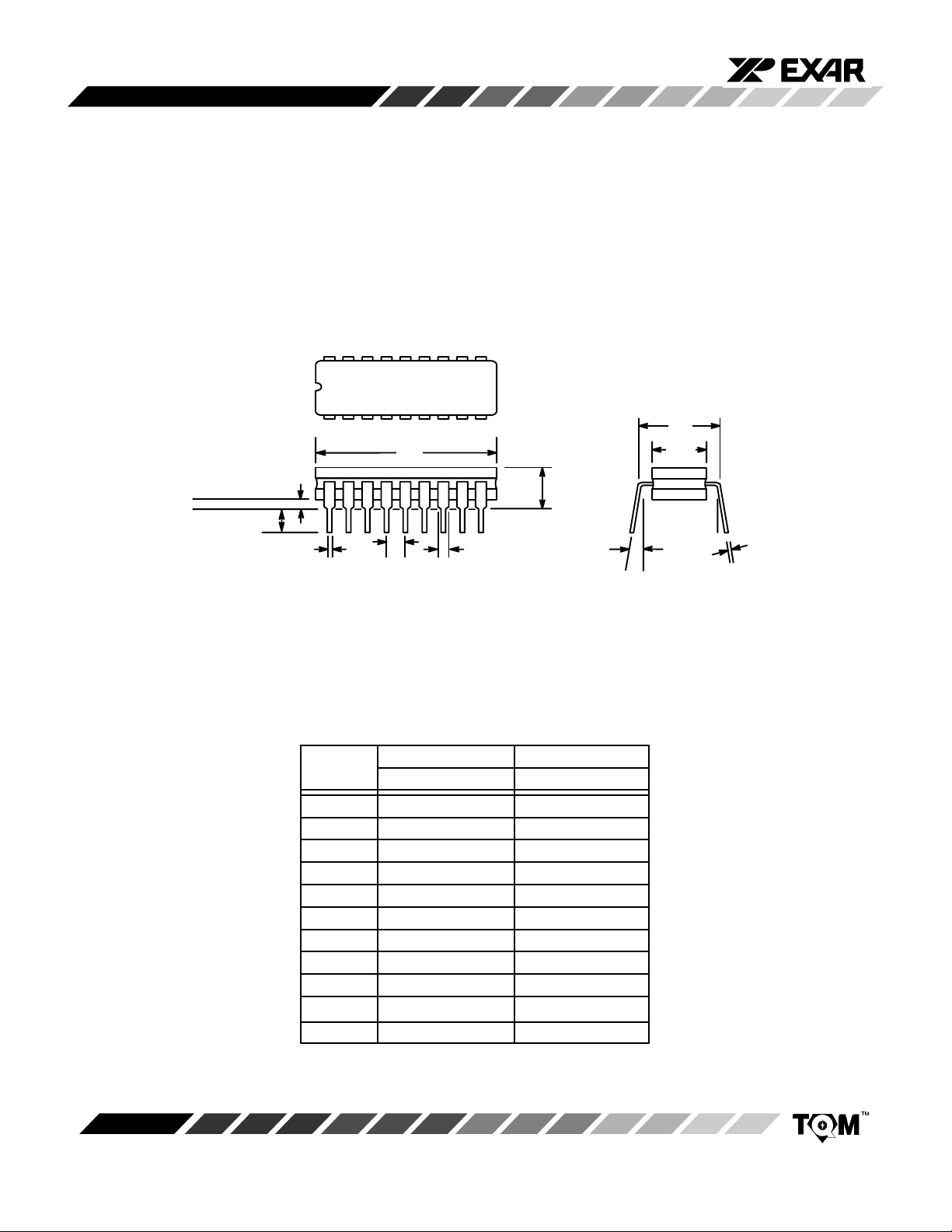
18 LEAD CERAMIC DUAL-IN-LINE
(300 MIL CDIP)
Rev. 1.00
Base
Plane
Seating
Plane
18
19
D
A
1
L
B
SYMBOL MIN MAX MIN MAX
A 0.100 0.200 2.54 5.08
A
1
B 0.014 0.026 0.36 0.66
B
1
c 0.008 0.018 0.20 0.46
D 0.860 0.960 21.84 24.38
E
1
E 0.300 BSC 7.62 BSC
e 0.100 BSC 2.54 BSC
L 0.125 0.200 3.18 5.08
e
INCHES MILLIMETERS
0.015 0.070 0.38 1.78
0.045 0.065 1.14 1.65
0.250 0.310 6.35 7.87
10
B
1
α 0° 15° 0° 15°
Note: The control dimension is the inch column
E
E
1
A
c
α
Rev. 2.01
8
Page 9
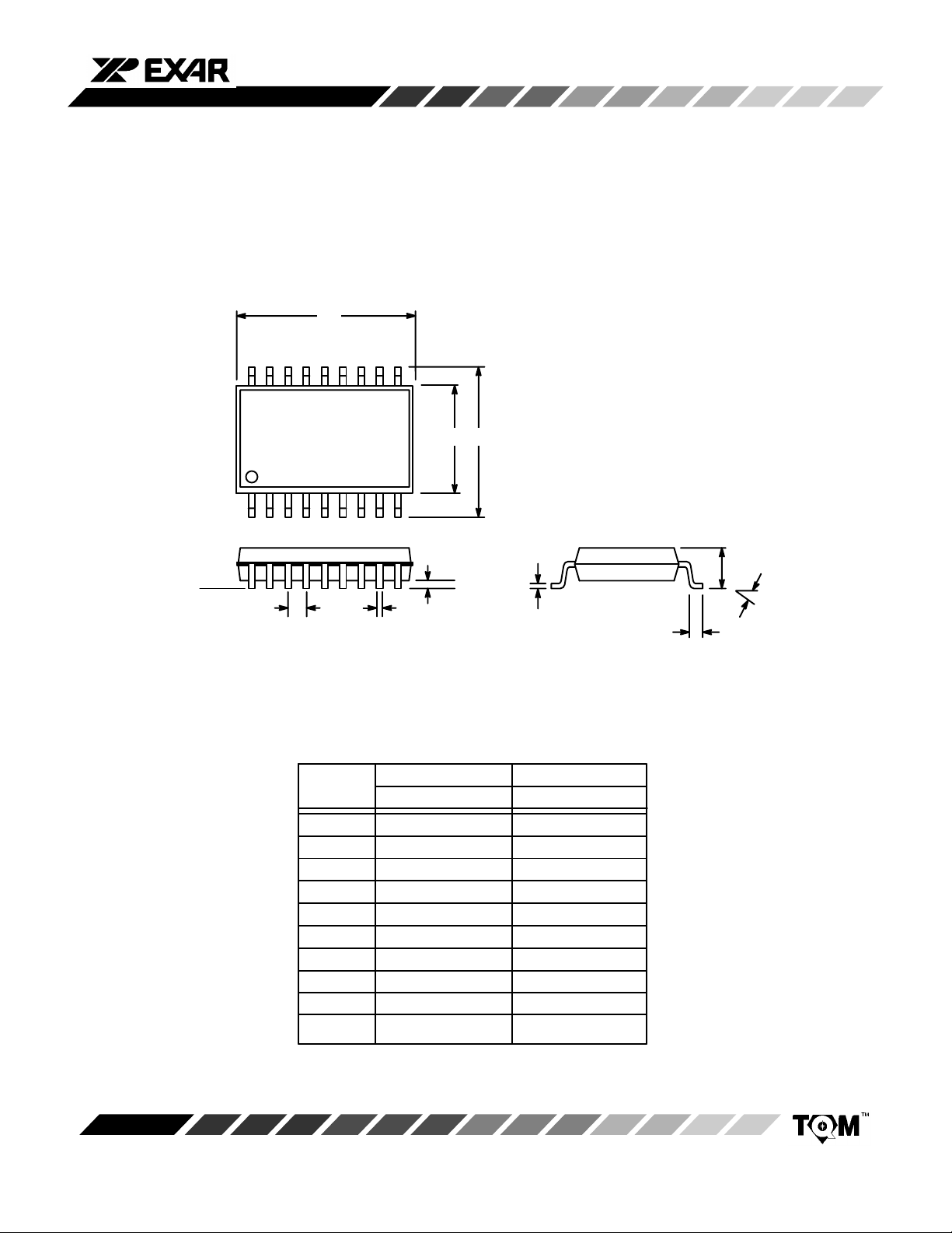
18 LEAD SMALL OUTLINE
(300 MIL JEDEC SOIC)
D
18 10
1
XR-T56L85
Rev. 1.00
E H
9
Seating
Plane
C
e
SYMBOL MIN MAX MIN MAX
A 0.093 0.104 2.35 2.65
A
1
B 0.013 0.020 0.33 0.51
C 0.009 0.013 0.23 0.32
D 0.447 0.463 11.35 11.75
E 0.291 0.299 7.40 7.60
e 0.050 BSC 1.27 BSC
H 0.394 0.419 10.00 10.65
L 0.016 0.050 0.40 1.27
B
A
1
INCHES MILLIMETERS
0.004 0.012 0.10 0.30
α 0° 8° 0° 8°
Note: The control dimension is the millimeter column
A
α
L
Rev. 2.01
9
Page 10

XR-T56L85
Notes
Rev. 2.01
10
Page 11

Notes
XR-T56L85
Rev. 2.01
11
Page 12

XR-T56L85
NOTICE
EXAR Corporation reserves the right to make changes to the products contained in this publication in order to improve design, performance or reliability . EXAR Corporation assumes no responsibility for the use of any circuits described herein, conveys no license under any patent or other right, and makes no representation that the circuits are
free of patent infringement. Charts and schedules contained here in are only for illustration purposes and may vary
depending upon a user’s specific application. While the information in this publication has been carefully checked;
no responsibility, however, is assumed for inaccuracies.
EXAR Corporation does not recommend the use of any of its products in life support applications where the failure or
malfunction of the product can reasonably be expected to cause failure of the life support system or to significantly
affect its safety or effectiveness. Products are not authorized for use in such applications unless EXAR Corporation
receives, in writing, assurances to its satisfaction that: (a) the risk of injury or damage has been minimized; (b) the
user assumes all such risks; (c) potential liability of EXAR Corporation is adequately protected under the circumstances.
Copyright 1992 EXAR Corporation
Datasheet June 1997
Reproduction, in part or whole, without the prior written consent of EXAR Corporation is prohibited.
Rev. 2.01
12
 Loading...