

Page 1
查询XR2207供应商
FEA TURES
...the analog plus company
TM
APPLICATIONS
XR-2207
Voltage-Controlled
Oscillator
June 1997–3
Excellent Temperature Stability (20ppm/°C)
Linear Frequency Sweep
Adjustable Duty Cycle (0.1% to 99.9%)
Two or Four Level FSK Capability
Wide Sweep Range (1000:1 Minimum)
Logic Compatible Input and Output Levels
Wide Supply Voltage Range (4V to 13V)
Low Supply Sensitivity (0.1% /V)
Wide Frequency Range (0.01Hz to 1MHz)
Simultaneous Triangle and Squarewave Outputs
GENERAL DESCRIPTION
The XR-2207 is a monolithic voltage-controlled oscillator
(VCO) integrated circuit featuring excellent frequency
stability and a wide tuning range. The circuit provides
simultaneous triangle and squarewave outputs over a
frequency range of 0.01Hz to 1MHz. It is ideally suited for
FM, FSK, and sweep or tone generation, as well as for
phase-locked loop applications.
FSK Generation
Voltage and Current-to-Frequency Conversion
Stable Phase-Locked Loop
Waveform Generation
– Triangle, Sawtooth, Pulse, Squarewave
FM and Sweep Generation
The XR-2207 has a typical drift specification of 20ppm/°C.
The oscillator frequency can be linearly swept over a
1000:1 range with an external control voltage; and the
duty cycle of both the triangle and the squarewave
outputs can be varied from 0.1% to 99.9% to generate
stable pulse and sawtooth waveforms.
ORDERING INFORMA TION
Part No. Package
XR-2207M 14 Lead 300 Mil CDIP -55°C to +125°C
XR-2207CP 14 Lead 300 Mil PDIP 0°C to +70°C
XR-2207D 16 Lead 300 Mil JEDEC SOIC 0°C to +70°C
XR-2207ID 16 Lead 300 Mil JEDEC SOIC -40°C to +85°C
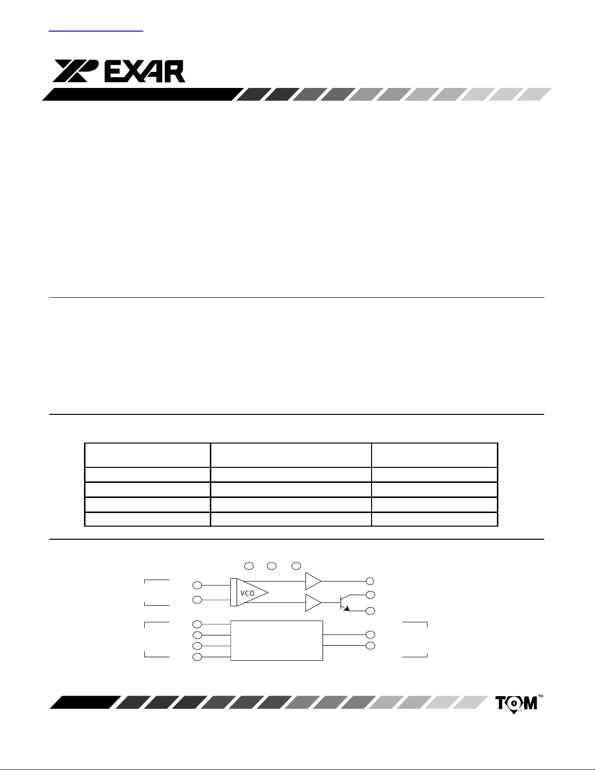
BLOCK DIAGRAM
Timing
Capacitor
Timing
Resistors
Rev. 2.02
1975
EXAR Corporation, 48720 Kato Road, Fremont, CA 94538 (510) 668-7000 FAX (510) 668-7017
C1
C1
R1
R2
R3
R4
Operating
T emperature Range
VCCGND BIAS
1
10 11
2
3
4
5
6
7
VCO
Current
Switches
A1
A2
14
13
SWO
12
V
9
BKI2
8
BKI1
Triangle Wave OutTWO
Square Wave Out
EE
Binary
Keying
Inputs
Figure 1. Block Diagram
1
Page 2
XR-2207
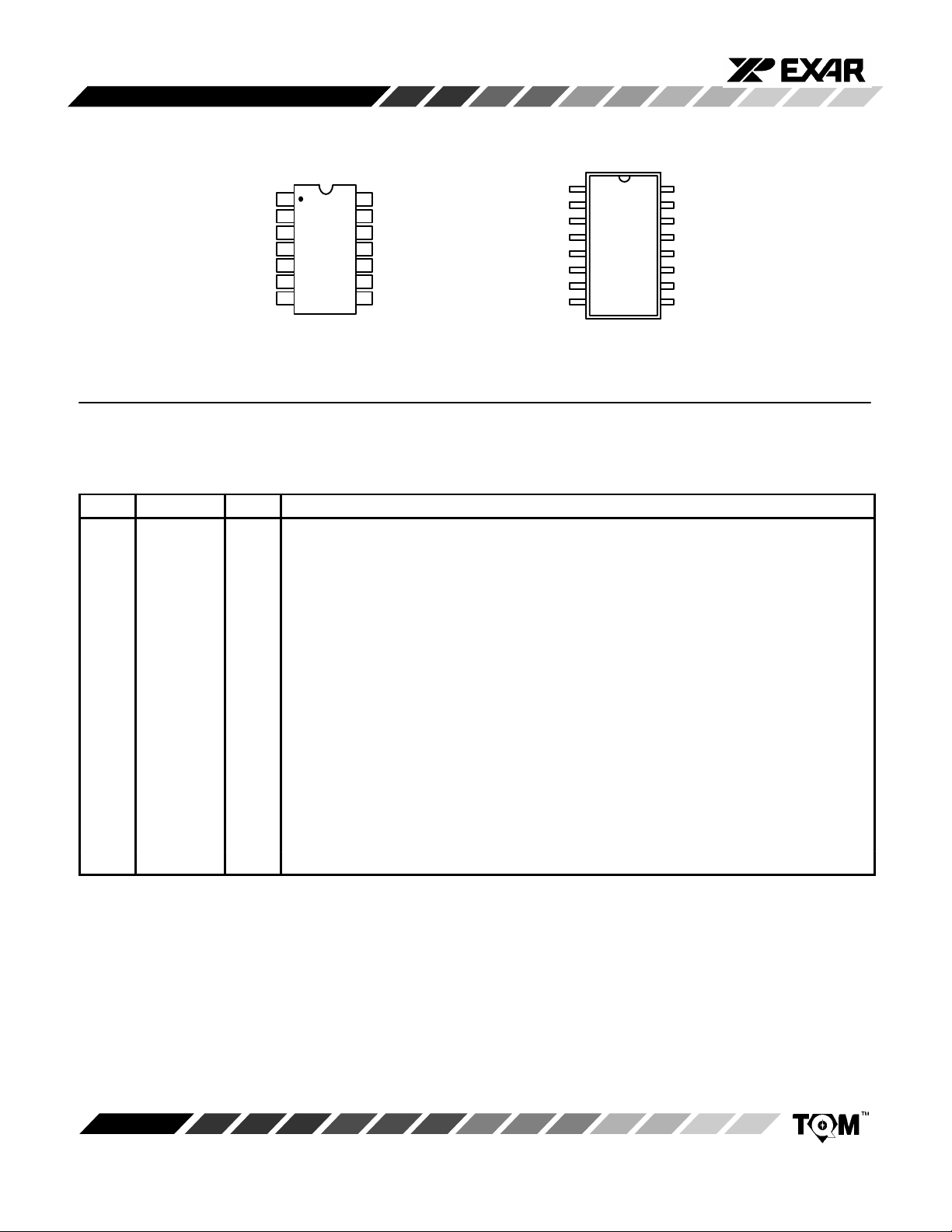
PIN CONFIGURATION
161
V
1
V
CC
2
C1
3
C2
4
R1
5
R2
6
R3
7
R4
14
TWO
13
SWO
12
V
EE
11
BIAS
10
GND
9
BKI2
8
BKI1
CC
C1
C2
R1
R2
R3
R4
BKI1
2
3
4
5
6
7
NC
15
NC
14
TWO
13
SWO
12
V
11
10
98
EE
BIAS
GND
BKI2
14 Lead PDIP, CDIP (0.300”)
PIN DESCRIPTION
Pin # Symbol Type Description
1 V
CC
2 C1 I Timing Capacitor Input.
3 C2 I Timing Capacitor Input.
4 R1 I Timing Resistor 1 Input.
5 R2 I Timing Resistor 2 Input.
6 R3 I Timing Resistor 3 Input.
7 R4 I Timing Resistor 4 Input.
8 BKI1 I Binary Keying 1 Timing Resistor Select Input.
9 BKI2 I Binary Keying 2 Timing Resistor Select Input.
10 GND Ground Pin.
11 BIAS I Bias Input for Single Supply Operation.
12 V
EE
13 SWO O Square Wave Output Signal.
14 TWO O Triangle Wave Output Signal.
15, 16 NC Only SOIC-16 Package.
Positive Power Supply.
Negative Power Supply .
16 Lead SOIC (Jedec, 0.300”)
Rev. 2.02
2
Page 3

XR-2207
P
Unit
Conditi
ELECTRICAL CHARACTERISTICS
Test Conditions: Test Circuit of
= R4 = 20kΩ, RL = 4.7kΩ, Binary Inputs Grounded, S1 and S2 Closed Unless Otherwise Specified
R
3
arameters
General Characteristics
Supply Voltage
Single Supply
Split Supplies
Supply Current See
Single Supply 5 7 5 8 mA Measure at Pin 1, S1, S
Split Supply See
Positive 5 7 5 8 mA Measure at Pin 1, S1, S
Negative 4 6 4 7 mA Measured at Pin 12, S1, S
Oscillator Section - Frequency Characteristics
Upper Frequency Limit 0.5 1.0 0.5 1.0 MHz C =500pF, R
Lowest Practical Frequency 0.01 0.01 Hz C =50µF, R3 = 2MΩ
Frequency Accuracy 1 3 1 5 % of f
Frequency Matching 0.5 0.5 % of f
Frequency Stability
Temperature
Power Supply
Sweep Range 1000:1 3000:1 1000:1 fH/f
Sweep Linearity % C =5000pF
10:1 Sweep
1000:1 Sweep
FM Distortion 0.1 0.1 % 10% FM Deviation
Recommended Range of
Timing Resistors
Impedance at Timing Pins 75 75 Ω Measured at Pins 4, 5, 6, or 7
DC Level at Timing Terminals 10 10 mV
Binary Keying Inputs
Switching Threshold 1.4 2.2 2.8 1.4 2.2 2.8 V Measured at Pins 8 and 9,
Input Impedance 5 5 kΩ
Figure 3
XR-2207ID/XR-2207M XR-2207CP/D
Min. T yp. Max. Min. Typ. Max.
8 26 8 26 V See
4 13 4 13 V See
and
Figure 4
, VCC = VEE = 6V, TA = +25°C, C = 5000pF, R1 = R2 =
s
ons
Figure 3
Figure 4
Figure 3
Open
Figure 4
Open
Open
= 2kΩ
3
O
O
20 50 30 ppm/°C 0°C < TA< 70°C
0.15 0.15 %V
R3 = 1.5kΩ for f
L
R3 = 2MΩ for f
1 2 1.5 fH=10kHz, fL= 1kHz
5 5 fH=100kHz, fL= 100Hz
1.5 2000 1.5 2000 kΩ See Characteristic Curves
Referenced to Pin 10
H1
L
2
2
2
Notes
Bold face parameters are covered by production test and guaranteed over operating temperature range.
Rev. 2.02
3
Page 4
XR-2207
P
Unit
Conditi
l
Linearity
ELECTRICAL CHARACTERISTICS (CONT’D)
XR-2207ID/XR-2207M XR-2207CP/D
arameters
Output Characteristics
Triangle Output Measured at Pin 13
Amplitude
Impedance
DC Leve
Squarewave Output Measured at Pin 13, S
Amplitude 11 12 11 12 Vpp
Saturation Voltage 0.2 0.4 0.2 0.4 V Referenced to Pin 12
Rise Time 200 200 nsec
Fall Time 20 20 nsec
Min. Typ. Max. Min. Typ. Max.
4 6 4 6 V
10 10 Ω
+100 +100 mV Referenced to Pin 10
0.1 0.1 % From 10% to 90% to Swing
s
PP
ons
Closed
CL 10pF
CL 10pF
2
Notes
Bold face parameters are covered by production test and guaranteed over operating temperature range.
Specifications are subject to change without notice
ABSOLUTE MAXIMUM RATINGS
Power Supply 26V. . . . . . . . . . . . . . . . . . . . . . . . . . . . . . .
Storage Temperature Range -65°C to +150°C. . . . .
Power Dissipation (package limitation)
Ceramic package 750mW. . . . . . . . . . . . . . . . . . . . . . .
Plastic package 625mW. . . . . . . . . . . . . . . . . . . . . . . . .
Derate above +25°C 5mW/°C. . . . . . . . . . . . . . . . . .
SOIC package 500mW. . . . . . . . . . . . . . . . . . . . . . . . .
Derate above +25°C 4mW/°C. . . . . . . . . . . . . . . . .
Derate above +25°C 6mW/°C. . . . . . . . . . . . . . . . . .
Rev. 2.02
4
Page 5
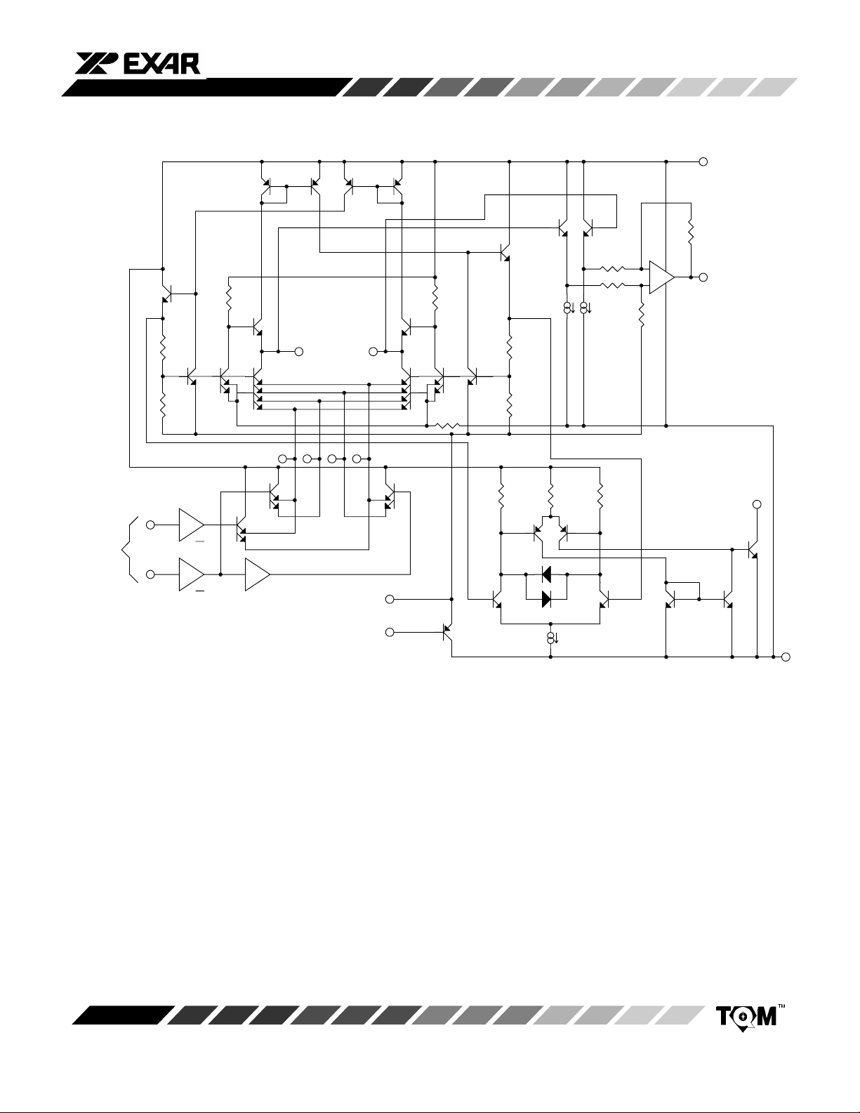
Q1 Q2 Q3 Q4
XR-2207
V
CC
1
Binary
Keying
Inputs
Q5
R1
Q6 Q7
R2
Timing Resistors
9
BB
8
AA
R
Q19
Capacitor
Q8 Q9
Q16
Q17
Timing
2
3
4567
Ground
BIAS
10
11
Q18
Q12
Q23
Q13
R
Q10 Q11
4R
Q22
Q14 Q15
R3
R4
Q20
R
R
R6R5 R7
Q21
Q24
–
+
2R
2R
14
Square Wave
Output
Q25 Q26
Triangle Wave
Output
13
Q27
V
EE
12
Rev. 2.02
Figure 2. Equivalent Schematic Diagram
5
Page 6
XR-2207
PRECAUTIONS
The following precautions should be observed when
operating the XR-2207 family of integrated circuits:
1. Pulling excessive current from the timing terminals
will adversely affect the temperature stability of the
circuit. To minimize this disturbance, it is
recommended that the total current drawn from pins
4, 5, 6, and 7 be limited to 6mA. In addition,
permanent damage to the device may occur if the
total timing current exceeds 10mA.
2. T erminals 2, 3, 4, 5, 6 , and 7 have very low internal
impedance and should, therefore, be protected from
accidental shorting to ground or the supply voltage.
3. The keying logic pulse amplitude should not exceed
the supply voltage.
SYSTEM DESCRIPTION
The XR-2207 functional blocks are shown in the block
diagram given in
Figure 1
. They are a voltage controlled
oscillator (VCO), four current switches which are
controlled by binary keying inputs, and two buffer
amplifiers for triangle and squarewave outputs.
Figure 2
is a simplified XR-2207 schematic diagram that shows the
circuit in greater detail.
The VCO is a modified emitter-coupled current controlled
multivibrator. Its oscillation is inversely proportional to the
value of the timing capacitor connected to pins 2 and 3,
and directly proportional to the total timing current IT. This
current is determined by the resistors that are connected
from the four timing terminals (pins 4, 5, 6 and 7) to
ground, and by the logic levels that are applied to the two
binary keying input terminals (pins 8 and 9). Four different
oscillation frequencies are possible since I
can have four
T
different values.
The triangle output buffer has a low impedance output
(10Ω TYP) while the squarewave is an open-collector
type. An external bias input allows the XR-2207 to be
used in either single or split supply applications.
V
CC
I+
C
0.1µF
C2
3
SWO
TWO
BIAS
12
Binary
Keying Inputs
0.1µF
8
9
10
S1
A
B
GND
2
1
C1
V+
XR-2207
R14R25R36R47V-
R2R1 R3 R4
Figure 3. Test Circuit for Single Supply Operation
13
14
11
RL
5.1K
3.9K
V
S2
Square Wave
Triangle Wave
CC
Output
Output
V
CC
Rev. 2.02
6
Page 7
V
CC
C
I+
0.1µF
C2
3
SWO
TWO
BIAS
12
0.1µF
S1
13
14
11
Binary
Keying Inputs
8
9
10
21
C1
V+
A
B
GND
XR-2207
R14R25R36R47V-
R2R1 R3 R4
Figure 4. Test Circuit for Split Supply Operation
RL
Triangle Wave
I-
V
CC
S2
Square Wave
Output
Output
V
EE
XR-2207
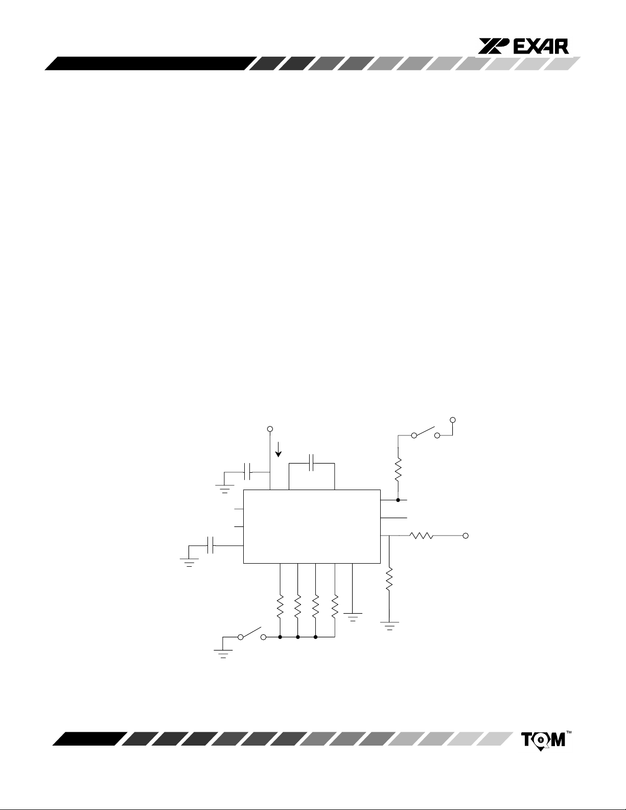
OPERA TING CONSIDERATIONS
Supply Voltage (Pins 1 and 12)
The XR-2207 is designed to operate over a power supply
range of 4V to 13V for split supplies, or 8V to 26V for
single supplies.
Figure 5
shows the permissible supply
voltage for operation with unequal split supply voltages.
Figure 6
and
Figure 7
show supply current versus supply
voltage Performance is optimum for 6V split supply , or
12V single supply operation. At higher supply voltages,
the frequency sweep range is reduced.
Ground (Pin 10)
For split supply operation, this pin serves as circuit
ground. For single supply operation, pin 10 should be AC
grounded through a 1µF bypass capacitor. During split
supply operation, a ground current of 2I
terminal, where I
is the total timing current.
T
flows out of this
T
Bias for Single Supply (Pin 11)
For single supply operation, pin 11 should be externally
+
biased to a potential between V
Figure 3
). The bias current at pin 1 1 is nominally 5% of the
total oscillation timing current, I
/3 and V+/2V (see
.
T
Bypass Capacitors
The recommended value for bypass capacitors is 1µF
although larger values are required for very low frequency
operation.
Timing Resistors (Pins 4, 5, 6, and 7)
The timing resistors determine the total timing current, I
available to charge the timing capacitor. Values for timing
resistors can range from 2kΩ to 2MΩ; however, for
optimum temperature and power supply stability,
recommended values are 4kΩ to 200kΩ (see
Figure 9, Figure 10
and
Figure 11
). T o avoid parasitic pick
Figure 8
up, timing resistor leads should be kept as short as
possible. For noisy environments, unused or deactivated
timing terminals should be bypassed to ground through
0.1µF capacitors.
Timing Capacitor (Pins 2 and 3)
The oscillator frequency is inversely proportional to the
timing capacitor, C. The minimum capacitance value is
limited by stray capacitances and the maximum value by
physical size and leakage current considerations.
Recommended values range from 100pF to 100µF. The
capacitor should be non-polarized.
,
T
,
Rev. 2.02
7
Page 8
XR-2207
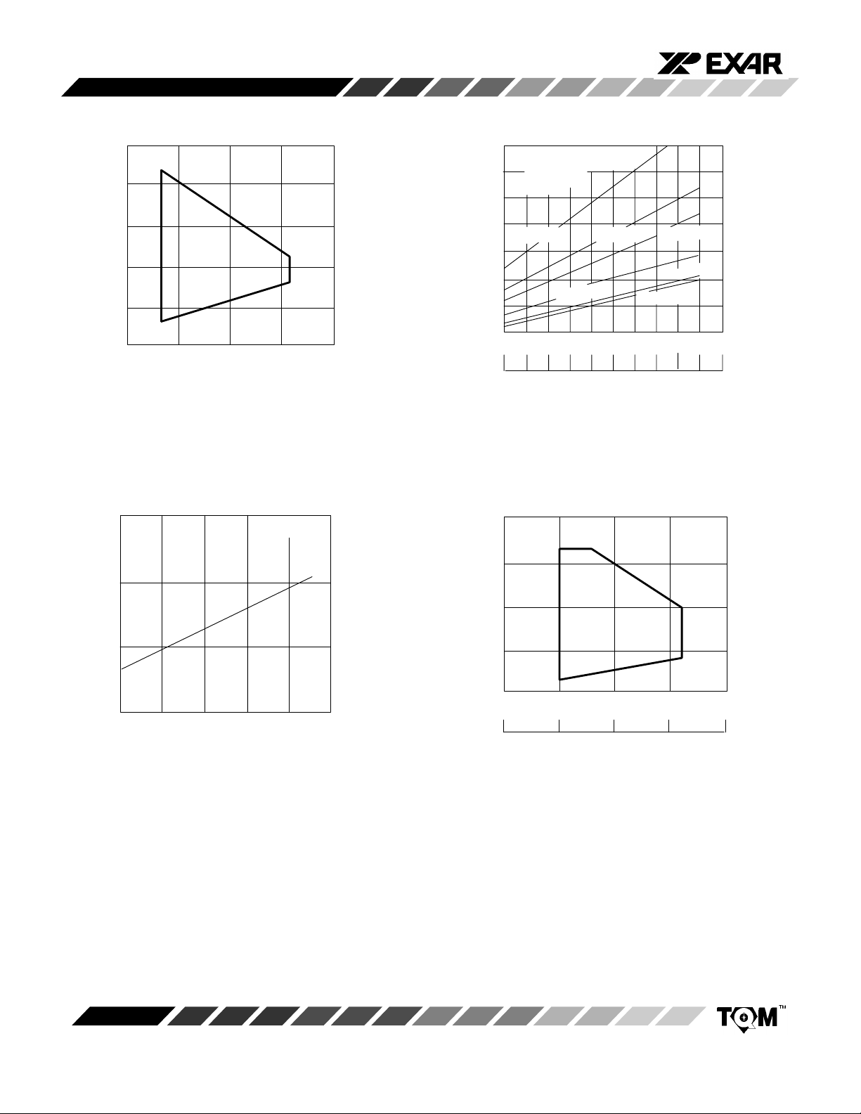
25
20
15
10
Positive Supply
5
0
Typical
Operating
Range
-5 -10 -15 -20
Negative Supply (V)
Figure 5. Operating Range for Unequal Split
Supply Voltages
15
TA=25°C
35
RT=Parallel Combination
30
25
20
15
10
Positive Supply (mA)
of Activated Timing
Resistors
=25°C
T
A
=5kΩ
R
R
T
T
R
T
=2MkΩ
RT=2kΩ RT=3kΩ
R
=20kΩ
5
0
4 6 8 10 12 14
810121416182022242628
T
Single Supply Voltage (V)
Figure 6. Positive Supply Current, 1
at Pin 1) vs. Supply Voltage
T
=200kΩ
+
(Measured
=25°C
A
10
5
Negative Supply Current (mA)
0
0 6 8 10 12 14
Split Supply Voltage (V)
Figure 7. Negative Supply Current, I
(Measured at Pin 12) vs. Supply Voltage
1MΩ
100kΩ
Timing
Resistor
10kΩ
Total T iming Resistor RT
1kΩ
0 8 16 24
-
Figure 8. Recommended Timing Resistor
Range
4V 8V 12V0
Single Supply Voltage (V)
Value vs. Power Supply Voltage
Rev. 2.02
8
Page 9

XR-2207
7
6
5
4
3
2
1
0
-1
-2
Frequency Error (%)
-3
-4
-5
-6
-7
1K 10K 100K 1M 10M
VS=6V
C=5000pF
Timing Resistance (Ω)
Figure 9. Frequency Accuracy vs.
Timing Resistance
+2%
+1%
0
-1%
4kΩ
20kΩ
200kΩ
2kΩ
V
=6V
S
C=5000pF
1.04
1.02
1.00
.98
.96
TA=25°C
R
Normalized Frequency Drift
T
.94
C=5000pF
.92
2 6 8 10 12 14
4 8 12 16 20 24 28
RT=2MΩ
=Total
Timing
Resistance
4
Split Supply Voltage (V)
Single Supply Voltage (V)
RT=20kΩ
RT=200kΩ
RT=2kΩ
Figure 10. Frequency Drift vs. Supply Voltage
2MΩ
200kΩ
20kΩ
4kΩ
Rev. 2.02
-2%
-3%
2MΩ
-50 -25 0 +25 +50 +75 +100 +125
Temperature (°C)
Normalized Frequency Drift (%)
Figure 11. Normalized Frequency Drift with
Temperature
9
R=2kΩ
Page 10

XR-2207
Timi
Binary Keying Inputs (Pins 8 and 9)
The logic levels applied to the two binary keying inputs
allow the selection of four different oscillator frequencies.
The internal impedance at these pins is approximately
5kΩ. Keying voltages, which are referenced to pin 10, are
< 1.4 V for “zero” and > 3V for “one” logic levels.
Table 1
relates binary keying input logic levels, and selected
timing pins to oscillator output frequency for each of the
four possible cases.
Figure 12
shows the oscillator control mechanism in
greater detail. Timing pins 4, 5, 6 and 7 correspond to the
emitters of switching transistor pairs T1, T2, T3, and T4
respectively, which are internal to the integrated circuit.
The current switches, and corresponding timing
terminals, are activated by external logic signals applied
to pins 8 and 9.
Logic Level Selected
Pin 8 Pin 9
0 0 6 f
0 1 6 and 7
1 0 5 f
1 1 4 and 5
ng Pins
Frequency
1
f1 + f
1
2
f2 + f
2
Table 1. Logic Table for Binary Keying Controls
Timing Capacitor
C
2
IT/2
A
B
8
9
Binary
Keying
Controls
45
I1 I2
R2R1 R3 R4
3
IT/2
T4
T3
T2
T1
67
I3 I4
12
V
CC
1
Ib
10
V
V
EE
Figure 12. Simplified Schematic of Frequency
Control Mechanism
Squarewave Output (Pin 13)
The squarewave output at pin 13 is an “open-collector”
stage capable of sinking up to 20mA of load current. R
serves as a pull-up load resistor for this output.
Recommended values for R
range from 1kΩ to 100kΩ.
L
Triangle Output (Pin 14)
L
Definitions:
f
1 +
1
R3C
f
1 +
1
R4C
f
2 +
1
R2C
f
2 +
1
R1C
Logic Levels: 0 = Ground, 1 3V
Note
For single supply operation, logic levels are referenced to
voltage at pin 10
Rev. 2.02
The output at pin 14 is a triangle wave with a peak swing of
approximately one-half of the total supply voltage. Pin 14
has a 10Ω output impedance and is internally protected
against short circuits.
MODES OF OPERA TION
Split Supply Operation
Figure 13
is the recommended configuration for split
supply operation. The circuit operates with supply
voltages ranging from $4V to $13V. Minimum drift
occurs with $6V supplies. For operation with unequal
supply voltages, see
With the generalized circuit of
Figure 5
.
Figure 13A
, the frequency
of operation is determined by the timing capacitor, C, and
the activated timing resistors (R
through R4). The timing
1
resistors are activated by the logic signals at the binary
10
Page 11

XR-2207
keying inputs (pins 8 and 9), as shown in the logic table
(
Table 1
). If a single timing resistor is activated, the
frequency is 1/RC. Otherwise, the frequency is either
||R2)C or 1/(R3||R4)C.
1/(R
1
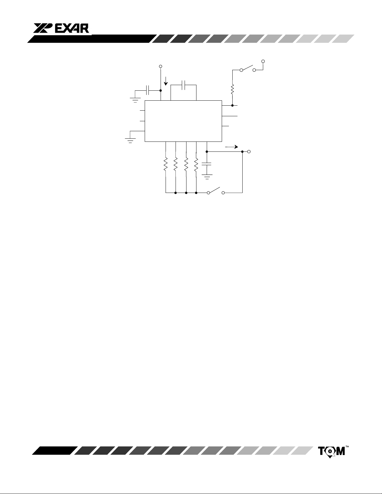
Figure 13B
shows a fixed frequency application using a
single timing resistor that is selected by grounding the
binary keying inputs. The oscillator frequency is 1/R
C.
3
The squarewave output is obtained at pin 13 and has a
V
CC
CB
1
C1
V+
8
Keying Inputs
CB = Bypass Cap
9
10
A
B
GND
XR-2207
R14R25R36R4
R2
peak-to-peak voltage swing equal to the supply voltages.
This output is an “open-collector” type and requires an
external pull-up load resistor (nominally 5kΩ) to the
positive supply . The triangle waveform obtained at pin 14
is centered about ground and has a peak amplitude of
+
V
/2.
Note
For Single-Supply Operation, Logic Levels are referenced to
voltage at Pin 10.
V
CC
C
RL
Square Wave
Output
Triangle Wave
Output
V
EE
C2
3
SWO
TWO
BIAS
7V-12
13
14
11
CB
2
R3 R4R1
V
EE
CB
8
9
10
CB = Bypass Cap
Figure 13. Split-Supply Operation
A. General Case
C
2
1
C
1
C
XR-2207
R14R25R36R4
R3
EE
3
2
SWO
TWO
BIAS
V-
712
A
B
GND
V
V+
CC
V
B. Fixed Frequency Case
CB
13
14
11
V
CC
RL
Square Wave
Output
Triangle Wave
Output
f=1/R3<C
V
EE
Rev. 2.02
11
Page 12

XR-2207
Single Supply Operation
The circuit should be interconnected as shown in
Figure 14A
12 should be grounded, and pin 11 biased from V
or
Figure 14B
for single supply operation. Pin
CC
through a resistive divider to a value of bias voltage
+
between V
/3 and V+/2. Pin 10 is bypassed to ground
through a 1µF capacitor.
V
CC
CB
8
CB
9
10
A
B
GND
XR-2207
R14R25R36R4
R3 R4R1
R2
Keying Inputs
CB = Bypass Cap
For single supply operation, the DC voltage at pin 10 and
the timing terminals (pins 4 through 7) are equal and
approximately 0.6V above V
, the bias voltage at pin 1 1.
B
The logic levels at the binary keying terminals are
referenced to the voltage at pin 10.
V
CC
C
RL
321
C2C1V+
SWO
TWO
BIAS
V-
712
13
14
11
3.9K
Square Wave
Output
Triangle Wave
Output
5.1K
V
CC
8
9
10
CB
CB = Bypass Cap
Figure 14. Single Supply Operation
A. General Case
CB
V
CC
2
1
V+
C1
A
B
GND
XR-2207
R14R25R36R47V-
R3
B. Single Frequency
V
CC
C
RL
C2
3
SWO
TWO
BIAS
12
13
14
11
5.1K
3.9K
Square Wave
Output
Triangle Wave
Output
V
CC
f=1/R3<C
Rev. 2.02
12
Page 13

XR-2207
Frequency Control (Sweep and FM)
The frequency of operation is controlled by varying the
total timing current, I
pins 4, 5, 6, or 7. The timing current can be modulated by
applying a control voltage, V
through a series resistor R
becomes more negative, both the total timing current, I
and the oscillation frequency increase.
The circuits given in
different frequency sweep methods for split supply
operation.
Both binary keying inputs are grounded for the circuit in
Figure 15
The frequency of operation, normally
proportional to the control voltage, V
as:
If R3 = 2MΩ, R
frequency sweep would result for a negative sweep
voltage V
The voltage to frequency conversion gain, K, is controlled
by the series resistance RC and can be expressed as:
. Therefore, only timing pin 6 is activated.
V-.
C
, drawn from the activated timing
T
, to the activated timing pin
C
. As the control voltage
C
Figure 15
1
f
+
R3C
= 2kΩ, C = 5000pF, then a 1000:1
C
ƪ
1 *
and
VCR
RCV-
Figure 16
, and determined
C
3
ƫ
Hz
f
+
show two
1
R3C
is now
The circuit of
negative values of control voltage. However, for positive
values of V
timing current I
Figure 16
where two timing pins, 6 and 7, are activated. The
frequency and the conversion gain expressions are the
,
T
same as before, except that the circuit will operate only
with negative values of V
deactivated and the frequency is fixed at:
The circuit given in
method for single supply operation. Here, the oscillation
frequency is given as:
where VT = Vbias + 0.7V.
This equation is valid from VC = 0V (RC is in parallel with
R3) to
Figure 15
with small (RC/R3) ratio, the direction of the
C
T
shows an alternate circuit for frequency control
f
+
can operate both with positive and
is reversed and the oscillations will stop.
. For VC > 0, pin 7 becomes
C
1
f
+
R
3
Figure 17
1
R3C
V
C
shows the frequency sweep
R
+
ƪ
1 )
V
T
R
ǒ
3
C
1 )
ǒ
1 *
V
C
Ǔ
ƫ
V
T
R
C
Ǔ
R
3
Rev. 2.02
+
f
V
C
K
+
1
RCCV-
HzńV
Caution
T otal timing current IT must be less than 6mA over the frequency
control range.
13
Page 14

XR-2207
1
f
ƪ
+
CR
1 *
3
VCR
RCV-
3
ƫ
CB = Bypass Cap
9
10
8
CB
A
B
GND
V
CC
C
C1V+
C2
XR-2207
456712
IT
IO
R3
V
IC
R
C
V
EE
C
Sweep or FM input
V
CC
4.7K
321
SWO
TWO
BIAS
V-R1 R2 R3 R4
V
13
14
11
C
Square Wave
Output
Triangle Wave
Output
V
EE
CB
Figure 15. Frequency Sweep Operation, Split Supply
V
CC
V
CC
CB
9
V+
A
B
GND
8
V
1
f
+
CR
VCR
ƪ
1 *
RCV-
3
CC
3
ƫ
CB = Bypass Cap
10
C
21
C1
XR-2207
456712
IO
R3
R
V
EE
3
C2
SWO
TWO
BIAS
V-R1 R2 R3 R4
IC
C
V
C
V
C
Sweep or FM input
13
14
11
4.7K
Square Wave
Triangle Wave
V
EE
CB
Output
Output
Rev. 2.02
Figure 16. Alternate Frequency Sweep Operation, Split Supply
14
Page 15

XR-2207
V
13
14
11
V
3.9K
EE
CC
4.7K
Vbias
Square Wave
Output
Triangle Wave
Output
5.1K
1µF
V
CC
V
CC
1µF
V+
8
A
R
3
1
f
ƪ
+
CR
1 )
RC
3
ǒ
1 *
VC
VT
1µF
9
10
B
GND
Ǔ
ƫ
C
21
C1
C2
XR-2207
R14R25R36R4
V
T
3
SWO
TWO
BIAS
V-
712
1µF
RC
VC+VC-
VC
Sweep or FM input
Figure 17. Frequency Sweep Operation, Single Supply
Duty Cycle Control
The duty cycle of the output waveforms can be controlled
by frequency shift keying at the end of every half cycle of
oscillator output. This is accomplished by connecting one
or both of the binary keying inputs (pins 8 or 9) to the
squarewave output at pin 13. The output waveforms can
then be converted to positive or negative pulses and
sawtooth waveforms.
Figure 18
is the recommended circuit connection for duty
cycle control. Pin 8 is shorted to pin 13 so that the circuit
switches between the “0,0” and the “1,0” logic states
given in
Table 1
. Timing pin 5 is activated when the output
is “high,” and the timing pin is activated when the
squarewave output goes to a low state.
The duty cycle of the output waveforms is given as:
R3
R
Duty Cycle
+
R
2 )R3
2
and can be varied from 0.1% to 99.9% by proper choice of
timing resistors. The frequency of oscillation, f, is given
as:
1
2
ƪ
f
+
R
C
2 )R3
ƫ
The frequency can be modulated or swept without
changing the duty cycle by connecting R
common control voltage V
Figure 15
). The sawtooth and the pulse output
waveforms are shown in
, instead of VEE (see
C
Figure 19
.
and R3 to a
2
Rev. 2.02
15
Page 16

XR-2207
8
10
9
CB
V
CC
21
V+
C1
A
B
GND
XR-2207
R14R25R36R47V-
4.7K
C
3
C2
R3R2
V
EE
SWO
TWO
BIAS
12
14
11
13
Pulse
Output
Sawtooth
Output
V
EE
CB
CB = Bypass Cap
V
CC
Figure 18. Duty Cycle Control
Rev. 2.02
16
Page 17

XR-2207
On-Off Keying
The XR-2207 can be keyed on and off by simply activating
an open circuited timing pin. Under certain conditions, the
circuit may exhibit very low frequency (<1Hz) residual
oscillations in the “off” state due to internal bias currents. If
this effect is undesirable, it can be eliminated by
connecting a 10MΩ resistor from pin 3 to V
CC
.
A. Squarewave and Triangle Outputs
B. Pulse and Sawtooth Outputs
Two-Channel FSK Generator (Modem Transmitter)
The multi-level frequency shift-keying capability of
XR-2207 makes it ideally suited for two-channel FSK
generation. A recommended circuit connection for this
application is shown in
Figure 20
.
For two-channel FSK generation, the “mark” and “space”
frequencies of the respective channels are determined by
the timing resistor pairs (R
“channel-select” control in accord with
“high” logic level at pin 8, the timing resistors R
, R2) and (R3, R4). Pin 8 is the
1
Figure 11
. For a
and R
1
are activated. Similarly, for a “low” logic level, timing
resistors R
and R4 are enabled.
3
The “high” and “low” logic levels at pin 9 determine the
respective high and low frequencies within the selected
FSK channel. When only a single FSK channel is used,
the remaining channel can be deactivated by connecting
pin 8 to either V
or ground. In this case, the unused
CC
timing resistors can also be omitted from the circuit.
2
C. Frequency Shift Keyed Outputs
Figure 19. Output Waveforms
Rev. 2.02
The low and high frequencies, f
and f2, for a given FSK
1
channel can be fine tuned using potentiometers
connected in series with respective timing resistors. In
fine tuning the frequencies, f
should be set first with the
1
logic level at pin 9 in a “low” level.
Typical frequency drift of the circuit for 0°C to 75°C
operation is $0.2%. Since the frequency stability is
directly related to the external timing components, care
must be taken to use timing components with low
temperature coefficients.
17
Page 18

XR-2207
f2
3V
OV
f1
Channel
Select
Keying
Input
10
8
9
1µF
V
CC
2
1
C1
V+
A
B
GND
XR-2207
R14R25R36R47V-
R1
R2
C
R3 R4
C2
3
SWO
TWO
BIAS
12
13
14
11
V
CC
RL
FSK
Output
f1 f2
1µF
10K 10K 10K 10K
Figure 20. Multi-Channel FSK Generation
V
EE
Rev. 2.02
18
Page 19

14 LEAD CERAMIC DUAL-IN-LINE
(300 MIL CDIP)
Rev. 1.00
XR-2207
Base
Plane
Seating
Plane
14
17
D
A
1
L
e
B
SYMBOL MIN MAX MIN MAX
A 0.100 0.200 2.54 5.08
A
1
B 0.014 0.026 0.36 0.66
B
1 0.045 0.065 1.14 1.65
c 0.008 0.018 0.20 0.46
D 0.685 0.785 17.40 19.94
E
1 0.250 0.310 6.35 7.87
E 0.300 BSC 7.62 BSC
e 0.100 BSC 2.54 BSC
L 0.125 0.200 3.18 5.08
0.015 0.060 0.38 1.52
8
A
1
B
INCHES MILLIMETERS
α 0° 15° 0° 15°
Note: The control dimension is the inch column
E
E
1
α
c
Rev. 2.02
19
Page 20

XR-2207
14 LEAD PLASTIC DUAL-IN-LINE
(300 MIL PDIP)
Rev. 1.00
Seating
Plane
14
1
D
A
L
B
SYMBOL MIN MAX MIN MAX
A 0.145 0.210 3.68 5.33
A
1
A
2
B 0.014 0.024 0.36 0.56
B
1
C 0.008 0.014 0.20 0.38
D 0.725 0.795 18.42 20.19
E 0.300 0.325 7.62 8.26
E
1
e 0.100 BSC 2.54 BSC
e
A
e
B
L 0.115 0.160 2.92 4.06
e
INCHES
0.015 0.070 0.38 1.78
0.115 0.195 2.92 4.95
0.030 0.070 0.76 1.78
0.240 0.280 6.10 7.11
0.300 BSC 7.62 BSC
0.310 0.430 7.87 10.92
8
E
1
7
A
1
B
1
MILLIMETERS
α 0° 15° 0° 15°
Note: The control dimension is the inch column
E
A
2
α
e
A
e
B
C
Rev. 2.02
20
Page 21

16 LEAD SMALL OUTLINE
(300 MIL JEDEC SOIC)
D
16 9
1
XR-2207
Rev. 1.00
E H
8
Seating
Plane
C
e
SYMBOL MIN MAX MIN MAX
A 0.093 0.104 2.35 2.65
A
1
B 0.013 0.020 0.33 0.51
C 0.009 0.013 0.23 0.32
D 0.398 0.413 10.10 10.50
E 0.291 0.299 7.40 7.60
e 0.050 BSC 1.27 BSC
H 0.394 0.419 10.00 10.65
L 0.016 0.050 0.40 1.27
α 0
Note: The control dimension is the millimeter column
B
A
1
INCHES MILLIMETERS
0.004 0.012 0.10 0.30
° 8° 0° 8°
A
α
L
Rev. 2.02
21
Page 22

XR-2207
Notes
Rev. 2.02
22
Page 23

Notes
XR-2207
Rev. 2.02
23
Page 24

XR-2207
NOTICE
EXAR Corporation reserves the right to make changes to the products contained in this publication in order to improve design, performance or reliability . EXAR Corporation assumes no responsibility for the use of any circuits described herein, conveys no license under any patent or other right, and makes no representation that the circuits are
free of patent infringement. Charts and schedules contained herein are only for illustration purposes and may vary
depending upon a user’s specific application. While the information in this publication has been carefully checked;
no responsibility, however, is assumed for inaccuracies.
EXAR Corporation does not recommend the use of any of its products in life support applications where the failure or
malfunction of the product can reasonably be expected to cause failure of the life support system or to significantly
affect its safety or effectiveness. Products are not authorized for use in such applications unless EXAR Corporation
receives, in writing, assurances to its satisfaction that: (a) the risk of injury or damage has been minimized; (b) the
user assumes all such risks; (c) potential liability of EXAR Corporation is adequately protected under the circumstances.
Copyright 1975 EXAR Corporation
Datasheet June 1997
Reproduction, in part or whole, without the prior written consent of EXAR Corporation is prohibited.
Rev. 2.02
24
 Loading...