

Page 1
XR2201
_____________________________ _________
1.2MHZ,26V Step-up DC/DC Converter
GENERAL DESCRIPTION
The XR2201 is a high frequency, high
efficiency DC to DC converter with an
integrated 2.8A, 0.1Ω power switch
capable of providing an output voltage up
to 26V. The fixed 1.2MHz allows the use
of small external inductions and
capacitors and provides fast transient
response. It integrates Soft start, Comp,.
only need few components outside.
FEATURES
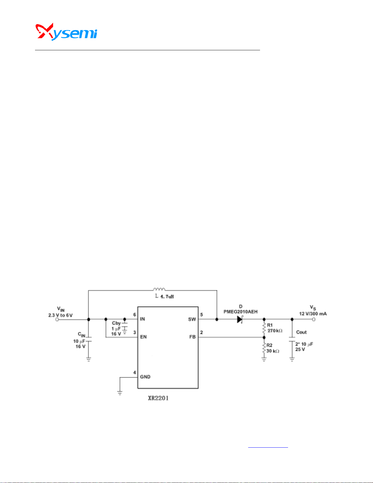
z 2.3V to 6V input voltage Rangel
z Efficiency up to 96%
z 26V Boost converter with 2.8A switch
current
z 1.2Mhz fixed Switching Frequency
z Integrated soft-start
z Thermal Shutdown
z Under voltage Lockout
z ESD 8KV Pass( HBM )
z 8-Pin MSOP Package
APPLICATIONS
• Handheld Devices
• GPS Receiver
• Digital Still Camera
• Portable Applications
• DSL Modem
• PCMCIA Card
• TFT LCD Bias Supply
Figure 1. Typical Application Circuit
XySemi Inc - 1 - www.xysemi.com
REV0.8
Page 2
XR2201
A
__________________________________________________________________________________________________
ORDERING INFORMATION
PART
NUMBER
XR2201 -40°C to 85°C 1.2MHZ
TEMP RANGE
SWICHING
FREQUENCY
OUTPUT
VOLTAGE (V)
DJ 2.8 MSOP 8
ILIM (A) PACKAGE PINS
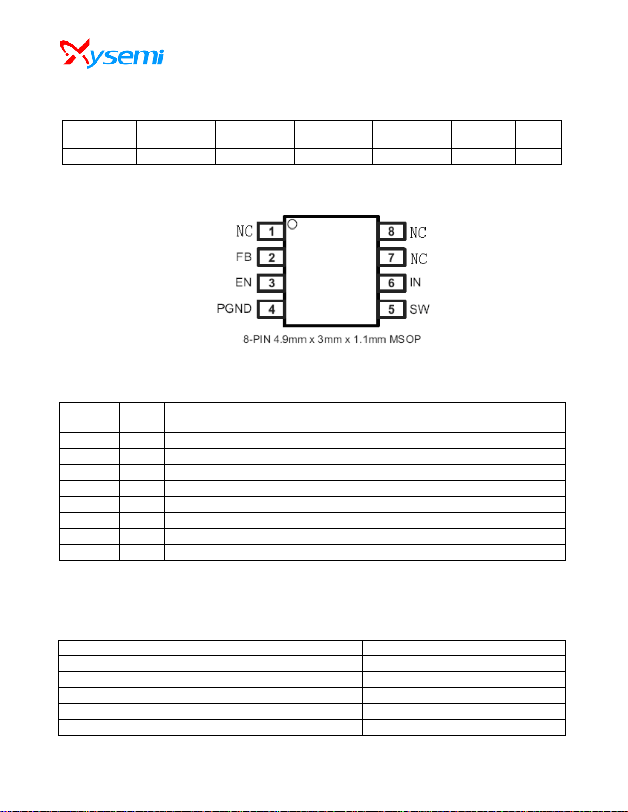
PIN CONFIGURATION
Figure 2. PIN Configuration
PIN DESCRIPTION
PIN
NUMBER
1 NC Not use
2 FB Feedback pin
3 EN Shutdown control input., Connect this pin to logic high level to enable the device
4 PGND Power ground
5 SW Switch pin
6 IN Input power supply pin
7 NC Not use
8 NC Not use
PIN
NAME
PIN DESCRIPTION
ABSOLUTE MAXIMUM RATINGS
(Note: Do not exceed these limits to prevent damage to the device. Exposure to absolute maximum rating
conditions for long periods may affect device reliability.)
PARAMETER VALUE UNIT
Supply Voltage VIN -0.3 to 6.5 V
FB, EN Voltage -0.3 to VIN+0.3 V
SW Voltage Vin+0.3 to 28V V
Operating Ambient Temperature
Maximum Junction Temperature 150 °C
XySemi Inc - 2 - www.xysemi.com
REV0.8
-40 to 85 °C
Page 3
XR2201
__________________________________________________________________________________________________
Storage Temperature -55 to 150 °C
Lead Temperature (Soldering, 10 sec) 300 °C
ELECTRICAL CHARACTERISTICS
(VIN = 3.6V, TA= 25°C unless otherwise specified)
PARAMETER SYMBOL TEST CONDITIONS MIN TYP MAX UNIT
Input Voltage Range V
2.3 6.0 V
IN
Boost output voltage range Vout 26 V
UVLO Threshold
V
Operating Supply Current
I
SUPPLY
Shutdown Supply Current
Regulated Feedback Voltage V
Peak Inductor Current I
Oscillator Frequency F
UVLO
FB
PEAK
OSC
V
HYSTERESIS
=1.3V,EN=Vin, I
V
FB
=100mV
Load
=0
VEN =0V, VIN =4.2V 0.1 1
1.188 1.2 1.212 V
2.5 2.8 3.0 A
0.9 1.2 1.5 MHz
2.1
2.2
2.3 V
75 135
µA
Rds(ON) of N-channel FET ISW =-100mA 0.1 0.2 Ohm
Enable Threshold VIN = 2.3V to 5.5V 0.3 1 1.5 V
Enable Leakage Current -0.1 0.1 µA
SW Leakage Current
VEN = 0V, VSW = 0V or 5V, VIN = 5V
1 uA
XySemi Inc - 3 - www.xysemi.com
REV0.8
Page 4
XR2201
__________________________________________________________________________________________________
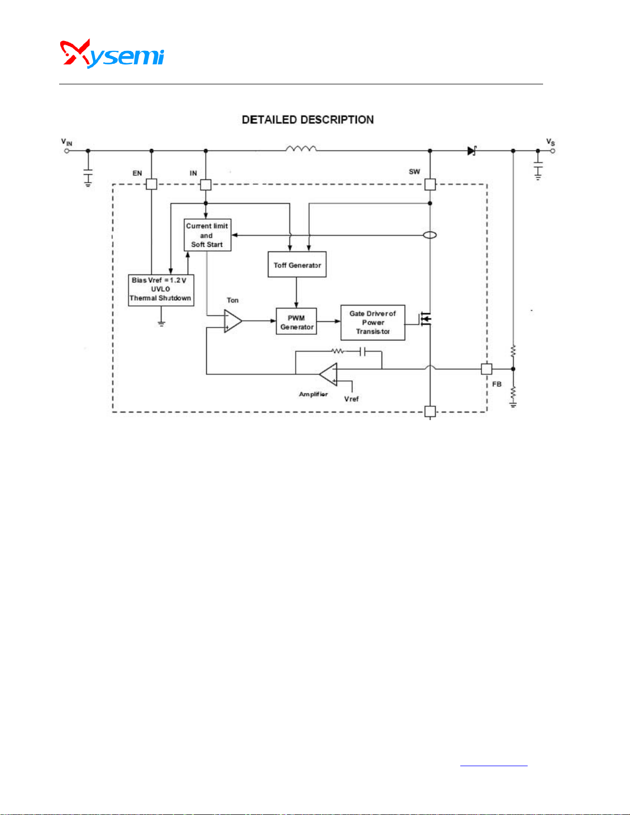
Figure 3. Functional Block Diagram
FUNCTIONAL DESCRIPTION
NORMAL OPERATION
The boost converter is designed for output
voltage up to 26V with a switch peak current limit of
2.8 A. The device, which operates in a current
mode scheme with quasi-constant frequency, is
externally 1.2MHZ and the minimum input voltage is
2.3 V. To control the inrush current at start-up a softstart pin is available.
During the on-time, the voltage across the
inductor causes the current in it to rise. When the
current reaches a threshold value set by the internal
GM amplifier, the power transistor is turned off, the
energy stored into the inductor is then released and
the current flows through the Schottky diode
towards the output of the boost converter. The offtime is fixed for a certain Vin and Vs, and therefore
maintains the same frequency when varying these
parameters.
drop across the Rdson of the power transistor
which will have an effect on the voltage across the
inductor and thus on
Some slight frequency changes might also appear
with a fixed output load due to the fact that the
output voltage Vs is not sensed directly but via the
SW Pin, which affects accuracy.
Because of the quasi-constant frequency
behavior of the device , the XR2201 eliminates the
need for an internal oscillator and slope
compensation, which provides better stability for the
system over a wide of input and output voltages
range, and more stable and accurate current
limiting operation compared to boost converters
operating with a conventional PWM scheme .The
XR2201 topology has also the benefits of providing
very good load and line regulations, and excellent
load transient response.
T (
T remains fixed).
on
off
However, for different output loads, the
frequency may slightly change due to the voltage
XySemi Inc - 4 - www.xysemi.com
REV0.8
Page 5

XR2201
__________________________________________________________________________________________________
UNDERVOLTAGE LOCKOUT (UVLO)
To avoid mis-operation of the device at low input
voltages an under voltage lockout is included that
disables the device, if the input voltage falls below
2.2V
THERMAL SHUTDOWN
A thermal shutdown is implemented to prevent
damages due to excessive heat and power
dissipation. Typically the thermal shutdown
threshold is 150℃ .When the thermal shutdown is
triggered the device stops switching until the
temperature falls below typically 136℃ .Then the
device starts switching again.
APPLICATION INFORMATION
INDUCTOR SELECTION
In normal operation, the inductor maintains continuous current to the output. The inductor current has
a ripple that is dependent on the inductance value. The high inductance reduces the ripple current.
Selected inductor by actual application:
Manufa
cturer
Murata
TDK
Part
Number
LQH44P
N
LQH5BP
SPM653
0T
VLP6045
LT
Induct
ance(u
H)
2.2 0.049
3.3 0.065
4.7 0.08
10 0.16
2.2 0.030
3.3 0.044
4.7 0.058
10 0.106
2.2 0017
3.3 0.027
4.7 0.036
2.2 0.020
3.3 0.025
DRC
max
(Ohms
)
Dimensions
L*W*H(mm3)
4*4*1.7
5*5*2
7.1*6.5*3
6*6*4.5
4.7 0.029
10 0.055
WURT
H
744373
24022
7447770
04
XySemi Inc - 5 - www.xysemi.com
REV0.8
2.2 0.061
4.7 0.025
4.4*4.05
7.3*7.3*4.5
Table 1. Recommend Surface Mount Inductors
Page 6

XR2201
__________________________________________________________________________________________________
If output voltage is 5V ,you can use 2.2uH~ 4.7uH, If output voltage is 12V, 4.7uH~ 10uH is OK,if 24V ,maybe
need 10uH
Normal application: Input 3.3V (3.6V or 4.2V) to Output 5V 9V 12V 24V;
Input 5V to Output 9V 12V 24V
Notes:Please select inductor according to I in. The IL need to be 1.5~2*I in. For getting higher efficiency, need to
use low DRC inductors.
INPUT CAPACITOR SELECTION
The input capacitor reduces input voltage ripple to the converter, low ESR ceramic capacitor is highly
recommended. For most applications, a 10uF capacitor is used. The input capacitor should be placed as close
as possible to VIN and GND. Such as Murata GRM21BR60J106 or TDK C3216X5R1A106M
OUTPUT CAPACITOR SELECTION
A low ESR output capacitor is required in order to maintain low output voltage ripple. In the case of ceramic
output capacitors, capacitor ESR is very small and does not contribute to the ripple, so a lower capacitance
value is acceptable when ceramic capacitors are used. A 10uF、22uF or two 10uF ceramic output capacitor is
suitable for most applications. Such as Murata GRM21BR60J226\ GRM21BR60J106 or TDK
C3216X5R1A226M\ C3216X5R1A106M
OUTPUT VOLTAGE PROGRAMMING
In the adjustable version, the output voltage is set by a resistive divider according to the following equation:
Typically choose R2=10K and determine R1 from the following equation:
DIODE SELECTION
According to max Iout and max Vout, you can select suitable diode. Normally we select diode
If=(1.5~2)*Ioutmax and VR=(1.5~2)*Voutmax. For high efficiency,suggest that you select low Vf Schottky
diode.
For example, 3.3V~4.2Vin 5V 1Aout,you can select MBRA210 or SS34. ONsemi’s MBRA210LT3 is prefer
XySemi Inc - 6 - www.xysemi.com
REV0.8
Page 7

XR2201
__________________________________________________________________________________________________
TYPICAL PERFORMANCE CHARACTERISTICS
(L=4.7uH, CIN=10uF, COUT=2*10uF,if not mentioned)
Efficiency vs. Output Current (Vout=5V)
Efficiency vs. Output Current(Vout=9V)
Efficiency vs. Output Current(Vout=12V)
STARTUP (3.3V IN 5V 500MA
XySemi Inc - 7 - www.xysemi.com
REV0.8
Page 8

XR2201
__________________________________________________________________________________________________
STARTUP (3.3V IN 5V 500MA OUT) STARTUP(3.3V IN 9V 500MA OUT)
PWM SWITCHING CONTINUOUS PWM SWITCHING DISCONTINUOUS
CONDUCTION MODE CONDUCTION MODE
NOTES:
The efficiency is tested under normal temperature, the actual current driver capability is 70%
~90% of the max current in sheet consider of high temperature surrounding status
XySemi Inc - 8 - www.xysemi.com
REV0.8
Page 9

XR2201
__________________________________________________________________________________________________
PACKAGE OUTLINE
MSOP8 PACKAGE OUTLINE AND DIMENSIONS
XySemi Inc - 9 - www.xysemi.com
REV0.8
Page 10

XR2201
__________________________________________________________________________________________________
PROUCT CHANGE NOTICE LIST
NO Updated date Version update Update content
1 2011-7-22 Rev 0.4 Update efficiency curve and some
electronic data
2 2011-8-24 Rev 0.4 Mend the efficiency curve description
error
3 2011-12-15 Rev 0.5 Update diode selection
4 2011-3-19 Rev 0.7 Update Inductor selection
5 2012-10-24 Rev 0.8 Update capacity selection
XySemi Inc - 10 - www.xysemi.com
REV0.8
Page 11

 Loading...