

Page 1

XR21V1410
1-CH FULL-SPEED USB UART
JUNE 2009 REV. 1.0.0
GENERAL DESCRIPTION
The XR21V1410 (V1410) is an enhanced Universal
Asynchronous Receiver and Transmitter (UART) with
a USB interface. The USB interface is fully compliant
to Full Speed USB 2.0 specification that supports 12
Mbps USB data transfer rate. The USB interface also
supports USB suspend, resume and remote wakeup
operations.
The V1410 operates from an internal 48MHz clock
therefore no external crystal/oscillator is required like
previous generation UARTs. With the fractional baud
rate generator, any baud rate can accurately be
generated using the internal 48MHz clock.
The large 128-byte FIFO and 384-byte RX FIFO of
the V1410 helps to optimize the overall data
throughput for various applications. The Automatic
Transceiver Direction control feature simplifies both
the hardware and software for half-duplex RS-485
applications. If required, the multidrop (9-bit) mode
with automatic half-duplex transceiver control feature
further simplifies typical multidrop RS-485
applications.
The V1410 operates from a single 2.97 to 3.63 volt
power supply and has 5V tolerant inputs. The V1410
is available in a 16-pin QFN package.
Software drivers for Windows 2000, XP, Vista, and
CE, as well as Linux and Mac are supported for the
XR21V1410.
FEATURES
• USB 2.0 Compliant Interface
■ Supports 12 Mbps USB full-speed data rate
■ Supports USB suspend, resume and remote
wakeup operations
• Enhanced UART Features
■ Data rates up to 12 Mbps
■ Fractional Baud Rate Generator
■ 128 byte TX FIFO
■ 384 byte RX FIFO
■ 7, 8 or 9 data bits, 1 or 2 stop bits
■ Automatic Hardware (RTS/CTS or DTR/DSR)
Flow Control
■ Automatic Software (Xon/Xoff) Flow Control
■ Multidrop mode w/ Auto Half-Duplex
Transceiver Control
■ Multidrop mode w/ Auto TX Enable
■ Half-Duplex mode
■ Sleep Mode with Remote Wake-up
■ Selectable GPIO or Modem I/O
• Internal 48 MHz clock
• Single 2.97-3.63V power supply
• 5V tolerant inputs
• 16-pin QFN package
APPLICATIONS
• Portable Appliances
• External Converters (dongles)
• Battery-Operated Devices
• Cellular Data Devices
• Factory Automation and Process Controls
• Industrial applications
• Virtual COM Port drivers
■ Windows 2000, XP and Vista
■ Windows CE 4.2, 5.0, 6.0
■ Linux
■ Mac
Exar Corporation 48720 Kato Road, Fremont CA, 94538 • (510) 668-7000 • FAX (510) 668-7017 • www.exar.com
Page 2
XR21V1410
1-CH FULL-SPEED USB UART REV. 1.0.0
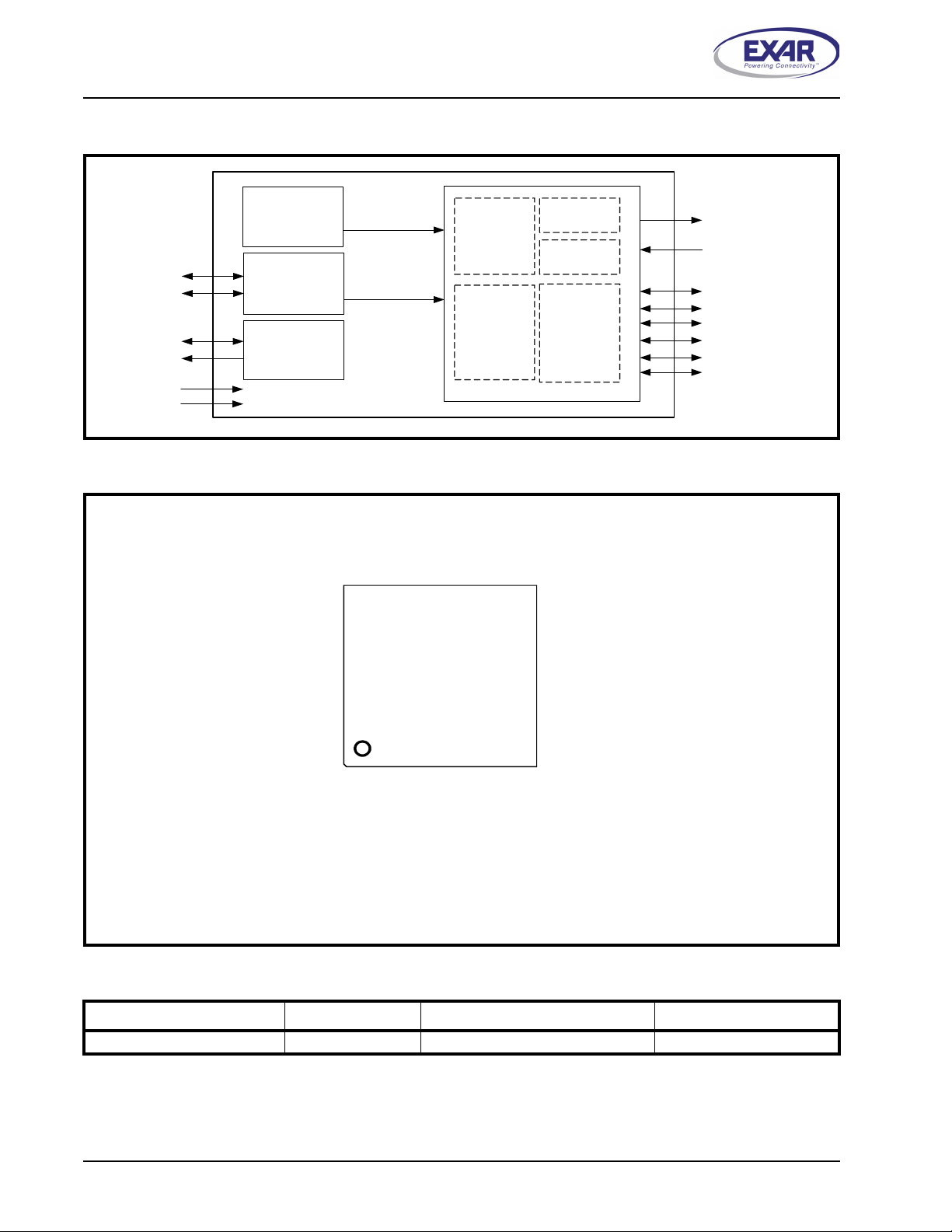
FIGURE 1. XR21V1410 BLOCK DIAGRAM
Internal
48MHz
Oscillator
USBD+
USBD-
SDA
SCL
3.3V VCC
GND
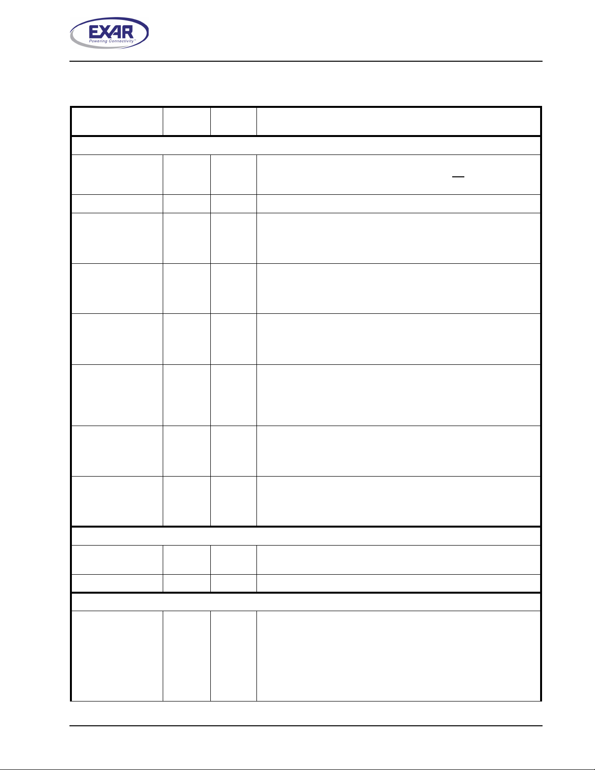
FIGURE 2. PIN OUT ASSIGNMENT
USB Slave
Interface
I2C
Interface
GND
SDA
SCL
12 11 10 9
13
Fractional
BRG
Internal
Status and
Control
Registers
RX
TX
8
128-byte
TX FIFO
384-byte
RX FIFO
GPIOs/
Modem IO
UART
GPIO0/RI#
TX
RX
GPIO5/RTS#
GPIO4/CTS#
GPIO3/DTR#
GPIO2/DSR#
GPIO1/CD#
GPIO0/RI#
USBD-
USBD+
ORDERING INFORMATION
PART NUMBER PACKAGE OPERATING TEMPERATURE RANGE DEVICE STATUS
XR21V1410IL16 16-pin QFN -40°C to +85°C Active
VCC
14
15
16-Pin
QFN
16
1234
GND
LOWPOWER
7
GPIO1/CD#
6
GPIO2/DSR#
5
GPIO3/DTR#
GPIO5/RTS#
GPIO4/CTS#
2
Page 3
XR21V1410
REV. 1.0.0 1-CH FULL-SPEED USB UART
PIN DESCRIPTIONS
Pin Description
NAME
UART Signals
RX 10 I
TX 9 O
GPIO0/RI#
GPIO1/CD#
GPIO2/DSR#
GPIO3/DTR#
GPIO4/CTS#
16-QFN
PIN #
8 I/O
7 I/O
6 I/O
5 I/O
4 I/O
TYPE DESCRIPTION
UART Channel A Receive Data or IR Receive Data. This pin has an
internal pull-up resistor. Internal pull-up resistor is
suspend mode.
UART Channel A Transmit Data or IR Transmit Data.
General purpose I/O or UART Ring-Indicator input (active low). This pin
has an internal pull-up resistor. Internal pull-up resistor is disabled during
suspend mode. If using this GPIO as an input, a pull-up resistor is
required to minimize the power consumption in the suspend mode.
General purpose I/O or UART Carrier-Detect input (active low). This pin
has an internal pull-up resistor. Internal pull-up resistor is disabled during
suspend mode. If using this GPIO as an input, a pull-up resistor is
required to minimize the power consumption in the suspend mode.
General purpose I/O or UART Data-Set-Ready input (active low). This
pin has an internal pull-up resistor. Internal pull-up resistor is disabled
during suspend mode. If using this GPIO as an input, a pull-up resistor
is required to minimize the power consumption in the suspend mode.
General purpose I/O or UART Data-Terminal-Ready output (active low).
This pin has an internal pull-up resistor. Internal pull-up resistor is dis
abled during suspend mode. If using this GPIO as an input, a pull-up
resistor is required to minimize the power consumption in the suspend
mode.
General purpose I/O or UART Clear-to-Send input (active low). This pin
has an internal pull-up resistor. Internal pull-up resistor is disabled during
suspend mode. If using this GPIO as an input, a pull-up resistor is
required to minimize the power consumption in the suspend mode.
not disabled during
-
GPIO5/RTS#
USB Interface Signals
USBD+ 15 I/O
USBD- 14 I/O
I2C Interface Signals
SDA 11 OD
3 I/O
General purpose I/O or UART Request-to-Send output (active low). This
pin has an internal pull-up resistor. Internal pull-up resistor is disabled
during suspend mode. If using this GPIO as an input, a pull-up resistor
is required to minimize the power consumption in the suspend mode.
USB port differential data plus. This pin has a 1.5 K Ohm internal pull-up
resistor.
USB port differential data minus.
I2C-controller data input/output (open-drain). 1K pull-up resistor is
required. An optional external I
default configurations upon power-up including the USB Vendor ID and
Device ID.
If an EEPROM is not used, this pin can be used with the SCL pin to
select the Remote Wake-up and Power modes. An external pull-up or
pull-down resistor is required. See
2
C EEPROM can be used to store
Table 1
3
Page 4

XR21V1410
1-CH FULL-SPEED USB UART REV. 1.0.0
Pin Description
NAME
SCL 12 I
Ancillary Signals
LOWPOWER
VCC
GND
NOTE: Pin type: I=Input, O=Output, I/O= Input/output, OD=Output Open Drain.
16-QFN
PIN #
2 O
16 Pwr
1, 13 Pwr
YPE DESCRIPTION
T
I2C-controller serial input clock. 1K pull-up resistor is required. An
optional external I
tions upon power-up including the USB Vendor ID and Device ID.
If an EEPROM is not used, this pin can be used with the SDA pin to
select the Remote Wake-up and Power modes. An external pull-up or
pull-down resistor is required. See Table 1
Low power status output. This pin is HIGH when the XR21V1410 is in
the suspend mode. This pin is LOW when the XR21V1410 is not in the
suspend mode. An external pull-up or pull-down resistor is required on
this pin. This pin is sampled upon power-on to configure the polarity of
the LOWPOWER output during suspend mode. An external pull-up
resistor will cause the LOWPOWER pin to be HIGH during suspend
mode. An external pull-down resistor will cause the LOWPOWER pin to
be LOW during suspend mode.
+3.3V power supply. All inputs are 5V tolerant.
Power supply common, ground.
2
C EEPROM can be used to store default configura-
4
Page 5
XR21V1410
REV. 1.0.0 1-CH FULL-SPEED USB UART
1.0 FUNCTIONAL DESCRIPTIONS
1.1 USB interface
The USB interface of the V1410 is compliant with the USB 2.0 Full-Speed Specifications. The USB
configuration model presented by the V1410 to the device driver is compatible to the Abstract Control Model of
the USB Communication Device Class (CDC-ACM). The V1410 uses the following set of parameters:
• 1 Control Endpoint
■ Endpoint 0 as outlined in the USB specifications
• 1 Configuration is supported
• 2 interfaces for the UART channel
■ Single interrupt endpoint
■ Bulk-in and bulk-out endpoints
1.1.1 USB Vendor ID
Exar’s USB Vendor ID is 0x04E2. This is the default Vendor ID that is used for the V1410 unless a valid
EEPROM is present on the I2C interface signals. If a valid EEPROM is present, the Vendor ID from the
EEPROM will be used.
1.1.2 USB Product ID
The default USB Product ID for the V1410 is 0x1410. If a valid EEPROM is present, the Product ID from the
EEPROM will be used.
1.2 I2C Interface
The I2C interface provides connectivity to an external I2C memory device (i.e. EEPROM) that can be read by
the V1410 for configuration.
The SDA and SCL are used to specify whether Remote Wakeup and/or Bus Powered configurations are to be
supported. These pins are sampled at power-up. The following table describes how Remote Wakeup and Bus
Powered support.
TABLE 1: REMOTE WAKEUP AND POWER MODES
SDA SCL
1 1 No Self-Powered Default, if no EEPROM is present
1 0 No Bus-Powered
0 1 Yes Self-Powered
0 0 Yes Bus-Powered
REMOTE WAKE-UP
UPPORT
S
POWER MODE COMMENTS
5
Page 6
XR21V1410
1-CH FULL-SPEED USB UART REV. 1.0.0
1.2.1 EEPROM Contents
The I2C address should be 0xA0. An EEPROM can be used to override default Vendor IDs and Device IDs, as
well as other attributes and maximum power consumption. The EEPROM must contain 8 bytes of data as
specified in
Table 2
TABLE 2: EEPROM CONTENTS
EEPROM
ADDRESS
0 Vendor ID (LSB)
1 Vendor ID (MSB)
2 Product ID (LSB)
3 Product ID (MSB)
4 Device Attributes
5 Device Maximum Power
6 Reserved
7 Signature of 0x58 (’X’). If the signature is not correct, the contents of the EEPROM are ignored.
CONTENTS
These values are uploaded from the EEPROM to the corresponding USB Standard Device Descriptor or
Standard Configuration Descriptor. For details of the USB Descriptors, refer to the USB 2.0 specifications.
1.2.1.1 Vendor ID
The Vendor ID value replaces the idVendor field in the USB Standard Device Descriptor.
1.2.1.2 Product ID
The Product ID value replaces the idProduct field in the USB Standard Device Descriptor.
1.2.1.3 Device Attributes
The Device Attributes value replaces the bmAttributes field in the USB Standard Configuration Descriptor.
1.2.1.4 Device Maximum Power
The Device Maximum Power value replaces the bMaxPower field in the USB Standard Configuration
Descriptor.
1.3 UART Manager
The UART Manager enables/disables the UART including the TX and RX FIFOs. The UART Manager is
located in a separate register block from the UART registers.
1.4 UART
The UART can be configured via USB control transfers from the USB host.
1.4.1 Transmitter
The transmitter consists of a 128-byte TX FIFO and a Transmit Shift Register (TSR). Once a bulk-out packet
has been received and the CRC has been validated, the data bytes in that packet are written into the TX FIFO
of the specified UART channel. Data from the TX FIFO is transferred to the TSR when the TSR is idle or has
completed sending the previous data byte. The TSR shifts the data out onto the TX output pin at the data rate
defined by the CLOCK_DIVISOR and TX_CLOCK_MASK registers. The transmitter sends the start bit
followed by the data bits (starting with the LSB), inserts the proper parity-bit if enabled, and adds the stopbit(s). The transmitter can be configured for 7 or 8 data bits with parity or 9 data bits with no parity.
1.4.1.1 9-Bit Data Mode
6
Page 7

XR21V1410
REV. 1.0.0 1-CH FULL-SPEED USB UART
In 9-bit data mode, two bytes of data must be written. The first byte that is loaded into the TX FIFO are the first
8 bits (data bits 7-0) of the 9-bit data. Bit-0 of the second byte that is loaded into the TX FIFO is bit-8 of the 9bit data. The data that is transmitted on the TX pin is as follows: start bit, 9-bit data, stop bit.
1.4.2 Receiver
The receiver consists of a 384-byte RX FIFO and a Receive Shift Register (RSR). Data that is received in the
RSR via the RX pin is transferred into the RX FIFO along with any error tags such as Framing, Parity, Break
and Overrun errors. Data from the RX FIFO can be sent to the USB host by sending a bulk-in packet.
1.4.2.1 Character Mode
In character mode, up to 64 bytes of data can be sent at a time to the USB host.
1.4.2.2 Character + Status Mode
In this mode, each 8-bit character and the 4 error bits associated with it can be transmitted to the USB host.
The 4 error bits will be in the second byte following the 8-bit character. In this mode, up to 32 character bytes
are sent per bulk-in packet.
1.4.2.3 9-Bit Data Mode
In 9-bit data mode, two bytes of data are sent to the USB host for each byte 9-bit data that is received. The first
byte sent to the USB host is the first 8-bits of data. Bit-0 of the second byte is the bit-9 of the data.
1.4.3 GPIO
Each UART has 6 GPIOs. By default, the GPIOs are general purpose I/Os. However, there are few modes
that can be enabled to add additional feature such as Auto RTS/CTS Flow control, Auto DTR/DSR Flow
Control or Transceiver Enable Control. See
1.4.4 Automatic RTS/CTS Hardware Flow Control
GPIO5 and GPIO4 of the UART channel can be enabled as the RTS# and CTS# signals for Auto RTS/CTS
flow control when GPIO_MODE[2:0] = ’001’ and FLOW_CONTROL[2:0] = ’001’. Automatic RTS flow control is
used to prevent data overrun errors in local RX FIFO by de-asserting the RTS signal to the remote UART.
When there is room in the RX FIFO, the RTS pin will be re-asserted. Automatic CTS flow control is used to
prevent data overrun to the remote RX FIFO. The CTS# input is monitored to suspend/restart the local
transmitter (see
Figure 3):
Table 13.
7
Page 8

XR21V1410
1-CH FULL-SPEED USB UART REV. 1.0.0
FIGURE 3. AUTO RTS AND CTS FLOW CONTROL OPERATION
Local UART
Receiver FIFO
Trigger Reached
Auto RTS
Trigger Level
Transmitter
Auto CTS
RTSA#
CTSB#
TXB
RXA FIFO
INTA
(RXA FIFO
Interrupt)
UARTA
Monitor
Data Starts
Assert RTS# to Begin
Transmission
1
2
3
4
Receive
Data
RX FIFO
Trigger Level
RXA TXB
RTSA# CTSB#
RXBTXA
RTSB#CTSA#
ON
ON
5
7
RTS High
Threshold
8
6
OFF
OFF
Suspend
Restart
9
RTS Low
Threshold
10
11
Remote UART
UARTB
Transmitter
Auto CTS
Monitor
Receiver FIFO
Trigger Reached
Auto RTS
Trigger Level
ON
ON
RX FIFO
12
Trigger Level
RTSCTS1
8
Page 9

XR21V1410
REV. 1.0.0 1-CH FULL-SPEED USB UART
1.4.5 Automatic DTR/DSR Hardware Flow Control
Auto DTR/DSR hardware flow control behaves the same as the Auto RTS/CTS hardware flow control
described above except that it uses the DTR# and DSR# signals. For Auto hardware flow control,
FLOW_CONTROL[2:0] = ’001’. GPIO3 and GPIO2 become DTR# and DSR#, respectively, when
GPIO_MODE[2:0] = ’010’.
1.4.6 Automatic XON/XOFF Software Flow Control
When software flow control is enabled, the V1410 compares the receive data characters with the programmed
Xon or Xoff characters. If the received character matches the programmed Xoff character, the V1410 will halt
transmission as soon as the current character has completed transmission. Data transmission is resumed
when a received character matches the Xon character. Software flow control is enabled when
FLOW_CONTROL[2:0] = ’010’.
1.4.7 Multidrop Mode with Automatic Half-Duplex Transceiver Control
Multidrop mode with Automatic Half-Duplex Transceiver Control is enabled when GPIO_MODE[2:0] = ’011’
and FLOW_CONTROL[2:0] = ’011’.
1.4.7.1 Receiver
In this mode, the UART Receiver will automatically be enabled when an address byte (9th bit or parity bit is ’1’)
is received that matches the value stored in the XON_CHAR or XOFF_CHAR register. The address byte will
not be loaded into the RX FIFO. All subsequent data bytes will be loaded into the RX FIFO. The UART
Receiver will automatically be disabled when an address byte is received that does not match the values in the
XON_CHAR or XOFF_CHAR register.
1.4.7.2 Transmitter
GPIO5/RTS# pin behaves as control pin for the direction of a half-duplex RS-485 transceiver. The polarity of
the GPIO5/RTS# pin can be configured via GPIO_MODE[3]. When the UART is not transmitting data, the
GPIO5/RTS# pin will be de-asserted. The GPIO5/RTS# pin will be asserted immediately before the UART
starts transmitting data. When the UART is done transmitting data, the GPIO5/RTS# pin will be de-asserted.
1.4.8 Multidrop Mode with Automatic Transmitter Enable
Multidrop mode with Automatic Transmitter Enable is enabled when GPIO_MODE[2:0] = ’100’ and
FLOW_CONTROL[2:0] = ’100’.
1.4.8.1 Receiver
The behavior of the receiver is the same in this mode as it is in the Address Match mode described above.
1.4.8.2 Transmitter
When there is an address match with the XON_CHAR register, the GPIO5/RTS# pin is asserted and remains
asserted whether the UART is transmitting data or not. The GPIO5/RTS# pin will be de-asserted when an
address byte is received that does not match the value in the XON_CHAR register. The polarity of the GPIO5/
RTS# pin can be configured via GPIO_MODE[3].
1.4.9 Programmable Turn-Around Delay
By default, the GPIO5/RTS# pin will be de-asserted immediately after the stop bit of the last byte has been
shifted. However, this may not be ideal for systems where the signal needs to propagate over long cables.
Therefore, the de-assertion of GPIO5/RTS# pin can be delayed from 1 to 15 bit times via the
XCVR_EN_DELAY register to allow for the data to reach distant UARTs.
1.4.10 Half-Duplex Mode
Half-duplex mode is enabled when FLOW_CONTROL[3] = 1. In this mode, the UART will ignore any data on
the RX input when the UART is transmitting data.
9
Page 10

XR21V1410
1-CH FULL-SPEED USB UART REV. 1.0.0
2.0 USB CONTROL COMMANDS
The following table shows all of the USB Control Commands that are supported by the V1410. Commands
included are standard USB commands, CDC-ACM commands and custom Exar commands. .
TABLE 3: SUPPORTED USB CONTROL COMMANDS
NAME
DEV GET_STATUS 0x80 0 0 0 0 0 2 0 Device: remote wake-up +
IF GET_STATUS 0x81 0 0 0 1-4,
EP GET_STATUS 0x82 0 0 0 0-4,
DEV CLEAR_FEATURE 0x00 1 1 0 0 0 0 0 Device remote wake-up
EP CLEAR_FEATURE 0x02 1 0 0 0-4,
DEV SET_FEATURE 0x00 3 1 00 0 0 0 0 Device remote wake-up
DEV SET_FEATURE 0x00 3 2 0 0 test 0 0 Tes t mo d e
EP SET_FEATURE 0x02 3 0 0 0-4,
REQUEST
YPE
T
REQUEST VALUE INDEX LENGTH DESCRIPTION
self-powered
0 2 0
129-
132
0 2 0
129-
136
0 0 0
129-
136
0 0 0
129-
136
Interface: zero
Endpoint: halted
Endpoint halt
Endpoint halt
SET_ADDRESS 0x00 5 addr 0 0 0 0 0
GET_DESCRIPTOR 0x80 6 0 1 0 0 len
LSB
GET_DESCRIPTOR 0x80 6 0 2 0 0 len
LSB
GET_CONFIGURATION 0x80 8 0 0 0 0 1 0
SET_CONFIGURATION 0x00 9 n 0 0 0 0 0
GET_INTERFACE 0x81 10 0 0 0-7 0 1 0
CDC_ACM_IF
SET_LINE_CODING
CDC_ACM_IF
GET_LINE_CODING
CDC_ACM_IF
SET_CONTROL_LINE_STATE
0x21 32 0 0 0, 2,
4, 6
0xA1 33 0 0 0, 2,
4, 6
0x21 34 val 0 0, 2,
4, 6
0 7 0 Set the UART baud rate,
0 7 0 Get the UART baud rate,
0 0 0
10
len
MSB
len
MSB
Device descriptor
Configuration descriptor
parity, stop bits, etc.
parity, stop bits, etc.
Set UART control lines
Page 11

XR21V1410
REV. 1.0.0 1-CH FULL-SPEED USB UART
TABLE 3: SUPPORTED USB CONTROL COMMANDS
NAME
CDC_ACM_IF
SEND_BREAK
XR_SET_REG 0x40 0 val 0 regis-
REQUEST
T
YPE
0x21 35 val
REQUEST VALUE INDEX LENGTH DESCRIPTION
LSB
val
MSB
0, 2,
4, 6
ter
0 0 0
block 0 0 Exar custom command: set
Send a break for the speci-
fied duration
one 8-bit register
val: 8-bit register value
register address: see
Table 6
block number: see Table 4
XR_GETN_REG 0xC0 1 0 0 regis-
ter
block count
LSB
count
MSB
Exar custom register: get
count 8-bit registers
register address: see
Table 6
block number: see Table 4
2.1 UART Block Numbers
The table below lists the block numbers for accessing each of the UART channels and the UART Manager..
TABLE 4: CONTROL BLOCKS
BLOCK NAME BLOCK NUMBER DESCRIPTION
UART 0 The configuration and control registers for UART.
Reserved 1-3 Block Numbers 1-3 are Reserved
UART Manager 4 The control registers for the UART Manager. The UART Manager
enables/disables the TX and RX FIFOs for each UART.
11
Page 12

XR21V1410
1-CH FULL-SPEED USB UART REV. 1.0.0
3.0 REGISTER SET DESCRIPTION
The internal register set of the V1410 consists of 2 different types of registers: UART Manager and UART
registers. The UART Manager controls the TX, RX and FIFOs of all UART channels. The UART registers
configure and control the remaining UART channel functionality not related to the UART FIFO.
3.1 UART Manager Registers.
.
TABLE 5: UART MANAGER REGISTERS
ADDRESS REGISTER NAME BIT-7 BIT-6 BIT-5 BIT-4 BIT-3 BIT-2 BIT-1 BIT-0
0X10 FIFO_ENABLE 0 0 0 0 0 0 RX TX
0X18 RX_FIFO_RESET Bit-7 Bit-6 Bit-5 Bit-4 Bit-3 Bit-2 Bit-1 Bit-0
0x1C TX_FIFO_RESET Bit-7 Bit-6 Bit-5 Bit-4 Bit-3 Bit-2 Bit-1 Bit-0
FIFO_ENABLE Registers
Enables the RX FIFO and TX FIFOs. For proper functionality, the UART TX and RX must be enabled in the
following order:
FIFO_ENABLE = 0x1 // Enable TX FIFO
UART_ENABLE = 0x3 // Enable TX and RX
FIFO_ENABLE = 0x3 // Enable RX FIFO
RX_FIFO_RESET and TX_FIFO_RESET Registers
Writing a non-zero value to these registers resets the FIFOs.
12
Page 13

XR21V1410
REV. 1.0.0 1-CH FULL-SPEED USB UART
3.2 UART Register Map
TABLE 6: UART REGISTERS
ADDRESS REGISTER NAME BIT-7 BIT-6 BIT-5 BIT-4 BIT-3 BIT-2 BIT-1 BIT-0
0X00 Reserved 0 0 0 0 0 0 0 0
0X01 Reserved 0 0 0 0 0 0 0 0
0X02 Reserved 0 0 0 0 0 0 0 0
0X03 UART_ENABLE 0 0 0 0 0 0 RX TX
0X04 CLOCK_DIVISOR0 Bit-7 Bit-6 Bit-5 Bit-4 Bit-3 Bit-2 Bit-1 Bit-0
0x05 CLOCK_DIVISOR1 Bit-15 Bit-14 Bit-13 Bit-12 Bit-11 Bit-10 Bit-9 Bit-8
0x06 CLOCK_DIVISOR2 0 0 0 0 0 Bit-18 Bit-17 Bit-16
0x07 TX_CLOCK_MASK0 Bit-7 Bit-6 Bit-5 Bit-4 Bit-3 Bit-2 Bit-1 Bit-0
0x08 TX_CLOCK_MASK1 Bit-15 Bit-14 Bit-13 Bit-12 Bit-11 Bit-10 Bit-9 Bit-8
0x09 RX_CLOCK_MASK0 Bit-7 Bit-6 Bit-5 Bit-4 Bit-3 Bit-2 Bit-1 Bit-0
0x0A RX_CLOCK_MASK1 Bit-15 Bit-14 Bit-13 Bit-12 Bit-11 Bit-10 Bit-9 Bit-8
0x0B CHARACTER_FORMAT Stop Parity Data Bits
0x0C FLOW_CONTROL
0x0D Reserved 0 0 0 0 0 0 0 0
0x0E Reserved 0 0 0 0 0 0 0 0
0x0F Reserved 0 0 0 0 0 0 0 0
0x10 XON_CHAR Bit-7 Bit-6 Bit-5 Bit-4 Bit-3 Bit-2 Bit-1 Bit-0
0x11 XOFF_CHAR Bit-7 Bit-6 Bit-5 Bit-4 Bit-3 Bit-2 Bit-1 Bit-0
0x12 Reserved 0 0 0 0 0 0 0 0
0x13 ERROR_STATUS Break
0x14 TX_BREAK Bit-7 Bit-6 Bit-5 Bit-4 Bit-3 Bit-2 Bit-1 Bit-0
0x15 XCVR_EN_DELAY 0 0 0 0 Delay
0x16 Reserved 0 0 0 0 0 0 0 0
0x17 Reserved 0 0 0 0 0 0 0 0
0x18 Reserved 0 0 0 0 0 0 0 0
0x19 Reserved 0 0 0 0 0 0 0 0
0 0 0 0
Status
Overrun
Error
Parity
Error
Framing
Error
Half-
Duplex
Break
Error
Flow Control Mode Select
0 0 0
0x1A GPIO_MODE
0 0 0 0
0x1B GPIO_DIRECTION 0 0 GPIO5 GPIO4 GPIO3 GPIO2 GPIO1 GPIO0
0x1D GPIO_SET 0 0 GPIO5 GPIO4 GPIO3 GPIO2 GPIO1 GPIO0
0x1E GPIO_CLEAR 0 0 GPIO5 GPIO4 GPIO3 GPIO2 GPIO1 GPIO0
0x1F GPIO_STATUS 0 0 GPIO5 GPIO4 GPIO3 GPIO2 GPIO1 GPIO0
XCVR
Enable
Polarity
Mode Select
13
Page 14

XR21V1410
1-CH FULL-SPEED USB UART REV. 1.0.0
3.3 UART Register Descriptions
3.3.1 UART_ENABLE Register Description (Read/Write)
This register enables the UART TX and RX. For proper functionality, the UART TX and RX must be enabled in
the following order:
FIFO_ENABLE = 0x1 // Enable TX FIFO
UART_ENABLE = 0x3 // Enable TX and RX of that channel
FIFO_ENABLE = 0x3 // Enable RX FIFO
UART_ENABLE[0]: Enable UART TX
• Logic 0 = UART TX disabled.
• Logic 1 = UART TX enabled.
UART_ENABLE[1]: Enable UART RX
• Logic 0 = UART RX disabled.
• Logic 1 = UART RX enabled.
UART_ENABLE[7:2]: Reserved
These bits are reserved and should remain ’0’.
3.3.2 CLOCK_DIVISOR0, CLOCK_DIVISOR1, CLOCK_DIVISOR2 Register Description (Read/Write)
These registers are used for programming the baud rate. The V1410 uses a 19-bit divisor and 16-bit mask
register. Using the internal 48MHz oscillator, the 19-bit divisor is calculated as follows:
CLOCK_DIVISOR = Trunc ( 48000000 / Baud Rate )
For example, if the the baud rate is 115200bps, then
CLOCK_DIVISOR = Trunc ( 48000000 / 115200 ) = Trunc (416.66667) = 416
CLOCK_DIVISOR0[7:0]: Baud rate clock divisor bits [7:0]
CLOCK_DIVISOR1[7:0]: Baud rate clock divisor bits [15:8]
CLOCK_DIVISOR2[2:0]: Baud rate clock divisor bits [18:16]
CLOCK_DIVISOR2[7:3]: Reserved
These bits are reserved and should remain ’0’.
3.3.3 TX_CLOCK_MASK0, TX_CLOCK_MASK1 Register Description (Read/Write)
A look-up table is used for the value of the 16-bit TX Clock mask registers. The index of the look-up table is
calculated as follows:
index = Trunc ( ( ( 48000000 / Baud Rate ) - CLOCK_DIVISOR ) * 32)
For example, if the baud rate is 115200bps, then the index will be:
index = Trunc ( ( ( 48000000 / 115200 ) - 416 ) * 32) = Trunc (21.3333) = 21
The values for some baud rates to program the TX_CLOCK_MASK registers are listed in Table 7. For baud
rates that are not listed, use the index to select TX_CLOCK_MASK register values from Ta b l e 8.
3.3.4 RX_CLOCK_MASK0, RX_CLOCK_MASK1 Register Description (Read/Write)
The values for some baud rates to program the RX_CLOCK_MASK registers are listed in Table 7. For baud
rates that are not listed, use the same index calculated for the TX_CLOCK_MASK register to select
RX_CLOCK_MASK register values from
Table 8.
14
Page 15

XR21V1410
REV. 1.0.0 1-CH FULL-SPEED USB UART
TABLE 7: CLOCK DIVISOR AND CLOCK MASK VALUES FOR COMMON BAUD RATES
BAUD RATE (BPS) CLOCK DIVISOR (DECIMAL) TX CLOCK MASK (HEX) RX CLOCK MASK (HEX)
1200 40000 0x0000 0x0000
2400 20000 0x0000 0x0000
4800 10000 0x0000 0x0000
9600 5000 0x0000 0x0000
19200 2500 0x0000 0x0000
38400 1250 0x0000 0x0000
57600 833 0x0912 0x0924
115200 416 0x0B6D 0x0B6A
230400 208 0x0912 0x0924
460800 104 0x0208 0x0040
500000 96 0x0000 0x0000
576000 83 0x0912 0x0924
921600 52 0x0040 0x0000
1000000 48 0x0000 0x0000
1152000 41 0x0B6D 0x0DB6
1500000 32 0x0000 0x0000
2000000 24 0x0000 0x0000
2500000 19 0x0104 0x0108
3000000 16 0x0000 0x0000
3125000 15 0x0492 0x0492
3500000 13 0x076D 0x0BB6
4000000 12 0x0000 0x0000
4250000 11 0x0122 0x0224
6250000 7 0x0B6D 0x0DB6
8000000 6 0x0000 0x0000
12000000 4 0x0000 0x0000
For baud rates that are not listed in the table above, use the index value calcuated using the formula in
“Section 3.3.3, TX_CLOCK_MASK0, TX_CLOCK_MASK1 Register Description (Read/Write)” on page 14
to determine which TX Clock and RX Clock Mask register values to use from Table 8. For the the RX Clock
Mask register, there are 2 values listed and would depend on whether the Clock Divisor is even or odd. For
even Clock Divisors, use the value from the first column. For odd Clock Divisors, use the value from the last
column.
15
Page 16

XR21V1410
1-CH FULL-SPEED USB UART REV. 1.0.0
TABLE 8: TX AND RX CLOCK MASK VALUES
INDEX
(DECIMAL)
0 0x0000 0x0000 0x0000
1 0x0000 0x0000 0x0000
2 0x0100 0x0000 0x0100
3 0x0020 0x0400 0x0020
4 0x0010 0x0100 0x0010
5 0x0208 0x0040 0x0208
6 0x0104 0x0820 0x0108
7 0x0844 0x0210 0x0884
8 0x0444 0x0110 0x0444
9 0x0122 0x0888 0x0224
10 0x0912 0x0448 0x0924
11 0x0492 0x0248 0x0492
12 0x0252 0x0928 0x0292
13 0x094A 0x04A4 0x0A52
14 0x052A 0x0AA4 0x054A
TX CLOCK MASK (HEX)
RX CLOCK MASK (HEX) -
EVEN CLOCK DIVISOR
RX CLOCK MASK (HEX) -
ODD CLOCK DIVISOR
15 0x0AAA 0x0954 0x04AA
16 0x0AAA 0x0554 0x0AAA
17 0x0555 0x0AD4 0x05AA
18 0x0B55 0x0AB4 0x055A
19 0x06B5 0x05AC 0x0B56
20 0x05B5 0x0D6C 0x06D6
21 0x0B6D 0x0B6A 0x0DB6
22 0x076D 0x06DA 0x0BB6
23 0x0EDD 0x0DDA 0x076E
24 0x0DDD 0x0BBA 0x0EEE
25 0x07BB 0x0F7A 0x0DDE
26 0x0F7B 0x0EF6 0x07DE
27 0x0DF7 0x0BF6 0x0F7E
28 0x07F7 0x0FEE 0x0EFE
29 0x0FDF 0x0FBE 0x07FE
30 0x0F7F 0x0EFE 0x0FFE
31 0x0FFF 0x0FFE 0x0FFD
16
Page 17

XR21V1410
REV. 1.0.0 1-CH FULL-SPEED USB UART
3.3.5 CHARACTER_FORMAT Register Description (Read/Write)
This register controls the character format such as the word length (7, 8 or 9), parity (odd, even, forced ’0’, or
forced ’1’) and number of stop bits (1 or 2).
CHARACTER_FORMAT[3:0]: Data Bits.
TABLE 9: DATA BITS
DATA BITS
7 0111
8 1000
9 1001
CHARACTER_FORMAT[3:0]
All other values for CHARACTER_FORMAT[3:0] are reserved.
CHARACTER_FORMAT[6:4]: Parity Mode Select
These bits select the parity mode. If 9-bit data mode has been selected, then writing to these bits will not have
any effect. In other words, there will not be an additional parity bit.
TABLE 10: PARITY SELECTION
BIT-6 BIT-5 BIT-4 PARITY SELECTION
0 0 0 No parity
0 0 1 Odd parity
0 1 0 Even parity
0 1 1 Force parity to mark, “1”
1 0 0 Force parity to space, “0”
CHARACTER_FORMAT[7]: Stop Bit select
This register selects the number of stop bits to add to the transmitted character and how many stop bits to
check for in the received character.
TABLE 11: STOP BIT SELECTION
BIT-7 NUMBER OF STOP BITS
0 1 stop bit
1 2 stop bits
3.3.6 FLOW_CONTROL Register Description (Read/Write)
These registers select the flow control mode. These registers should only be written to when the UART is
disabled. Writing to the FLOW_CONTROL register when the UART is enabled will result in undefined
behavior.
17
Page 18

XR21V1410
1-CH FULL-SPEED USB UART REV. 1.0.0
FLOW_CONTROL[2:0]: Flow control mode select
TABLE 12: FLOW CONTROL MODE SELECTION
BIT-2 BIT-1 BIT-0 MODE DESCRIPTION
0 0 0 No flow control.
0 0 1 HW flow control enabled
0 1 0 SW flow control enabled
0 1 1 Multidrop mode with Automatic Half-Duplex Transceiver control
1 0 0 Multidrop mode with Automatic Transmitter Enable
FLOW_CONTROL[3]: Half-Duplex Mode
• Logic 0 = Normal (full-duplex) mode. The UART can transmit and receive data at the same time.
• Logic 1 = Half-duplex Mode. In half-duplex mode, any data on the RX pin is ignored when the UART is
transmitting data.
FLOW_CONTROL[7:4]: Reserved
These bits are reserved and should remain ’0’.
3.3.7 XON_CHAR, XOFF_CHAR Register Descriptions (Read/Write)
The XON_CHAR and XOFF_CHAR registers store the XON and XOFF characters, respectively, that are used
in the Automatic Software Flow control.
XON_CHAR[7:0]: XON Character
In Automatic Software Flow control mode, the UART will resume data transmission when the XON character
has been received.
For behavior in the Address Match mode, see “Section 1.4.7, Multidrop Mode with Automatic Half-Duplex
Transceiver Control” on page 9.
For behavior in the Address Match with TX Flow Control mode, see “Section 1.4.8, Multidrop Mode with
Automatic Transmitter Enable” on page 9.
XOFF_CHAR[7:0]: XOFF Character
In Automatic Software Flow control mode, the UART will suspend data transmission when the XOFF character
has been received.
For behavior in the Address Match mode, see “Section 1.4.7, Multidrop Mode with Automatic Half-Duplex
Transceiver Control” on page 9.
For behavior in the Address Match with TX Flow Control mode, see “Section 1.4.8, Multidrop Mode with
Automatic Transmitter Enable” on page 9.
3.3.8 ERROR_STATUS Register Description - Read-only
This register reports any errors that may have occurred on the line such as break, framing, parity and overrun.
ERROR_STATUS[2:0]: Reserved
These bits are reserved. Any values read from these bits should be ignored.
ERROR_STATUS[3]: Break error
• Logic 0 = No break condition
• Logic 1 = A break condition has been detected (clears after read).
18
Page 19

XR21V1410
REV. 1.0.0 1-CH FULL-SPEED USB UART
ERROR_STATUS[4]: Framing Error
• Logic 0 = No framing error
• Logic 1 = A framing error has been detected (clears after read). A framing error occurs when a stop bit is not
present when it is expected.
ERROR_STATUS[5]: Parity Error
• Logic 0 = No parity error
• Logic 1 = A parity error has been detected (clears after read).
ERROR_STATUS[6]: Overrun Error
• Logic 0 = No overrun error
• Logic 1 = An overrun error has been detected (clears after read). An overrun error occurs when the RX FIFO
is full and another byte of data is received.
ERROR_STATUS[7]: Break Status
• Logic 0 = Break condition is no longer present.
• Logic 1 = Break condition is currently being detected.
3.3.9 TX_BREAK Register Description (Read/Write)
Writing a non-zero value to this register causes a break condition to be generated continuously until the
register is cleared. If data is being shifted out of the TX pin, the data will be completed shifted out before the
break condition is generated.
3.3.10 XCVR_EN_DELAY Register Description (Read/Write)
XCVR_EN_DELAY[3:0]: Turn-around delay
This is the number of bit times to wait before changing the direction of the transceiver from transmit to receive
when half-duplex mode is enabled.
XCVR_EN_DELAY[3:0]: Reserved
These bits are reserved and should be ’0’.
3.3.11 GPIO_MODE Register Description (Read/Write)
GPIO_MODE[2:0]: GPIO Mode Select
There are 4 modes of operation for the GPIOs. The descriptions can be found in “Section 1.4, UART” on
page 6.
TABLE 13: GPIO MODES
BITS
[2:0]
000 GPIO0 GPIO1 GPIO2 GPIO3 GPIO4 GPIO5 GPIO Mode
001 GPIO0 GPIO1 GPIO2 GPIO3 CTS# RTS# Auto RTS/CTS HW Flow Control
GPIO0 GPIO1 GPIO2 GPIO3 GPIO4 GPIO5
MODE DESCRIPTION
010 GPIO0 GPIO1 DSR# DTR# GPIO4 GPIO5 Auto DTR/DSR HW Flow Control
011 GPIO0 GPIO1 GPIO2 GPIO3 GPIO4 XCVR
Enable
100 GPIO0 GPIO1 GPIO2 GPIO3 GPIO4 XCVR
Enable
19
Multidrop Mode with Auto Half-Duplex Transceiver Control
Multidrop Mode with Auto TX Enable
Page 20

XR21V1410
1-CH FULL-SPEED USB UART REV. 1.0.0
GPIO_MODE[3]: Transceiver Enable Polarity
• Logic 0 = Low for TX
• Logic 1 = High for TX
GPIO_MODE[7:4]: Reserved
These register bits are reserved. When writing to these bits, the value should be ’0’. When reading from these
bits, they are undefined and should be ignored.
3.3.12 GPIO_DIRECTION Register Description (Read/Write)
This register controls the direction of the GPIO if it is not controlled by the GPIO_MODE register.
GPIO_DIRECTION[5:0]: GPIOx Direction
• Logic 0 = GPIOx is an input.
• Logic 1 = GPIOx is an output.
GPIO_DIRECTION[7:6]: Reserved
These register bits are reserved and should be ’0’.
3.3.13 GPIO_SET Register Description (Read/Write)
Writing a ’1’ in this register drives the GPIO output high. Writing a ’0’ to a bit has no effect. Bits 7-6 are unused
and should be ’0’.
3.3.14 GPIO_CLEAR Register Description (Read/Write)
Writing a ’1’ in this register drives the GPIO output low. Writing a ’0’ to a bit has no effect. Bits 7-6 are unused
and should be ’0’.
3.3.15 GPIO_STATUS Register Description (Read-Only)
This register reports the current state of the GPIO pin.
20
Page 21

XR21V1410
REV. 1.0.0 1-CH FULL-SPEED USB UART
4.0 ELECTRICAL CHARACTERISTICS
DC ELECTRICAL CHARACTERISTICS - POWER CONSUMPTION
UNLESS OTHERWISE NOTED: TA = -40O TO +85OC, VCC IS 2.97 TO 3.63V
LIMITS
SYMBOL PARAMETER
3.3V
MIN TYP MAX
I
CC
I
Susp
Power Supply Current 16 20 mA
Suspend mode Current 2 2.15 mA
DC ELECTRICAL CHARACTERISTICS - UART & GPIO PINS
UNLESS OTHERWISE NOTED: TA = -40O TO +85OC, VCC IS 2.97 TO 3.63V
LIMITS
SYMBOL PARAMETER
V
IL
V
IH
V
OL
V
OH
I
IL
I
IH
C
IN
Input Low Voltage -0.3 0.8 V
Input High Voltage 2.0 5.5 V
Output Low Voltage 0.3 V IOL = 4 mA
Output High Voltage 2.2 V IOH = -4 mA
Input Low Leakage Current ±10 uA
Input High Leakage Current ±10 uA
Input Pin Capacitance 5 pF
3.3V
MIN MAX
UNITS CONDITIONS
UNITS CONDITIONS
DC ELECTRICAL CHARACTERISTICS - USB I/O PINS
UNLESS OTHERWISE NOTED: TA = -40O TO +85OC, VCC IS 2.97 TO 3.63V
LIMITS
SYMBOL PARAMETER
V
V
V
V
I
OSC
V
IL
IH
OL
OH
DrvZ
Input Low Voltage -0.3 0.8 V
Input High Voltage 2.0 5.5 V
Output Low Voltage 0 0.3 V External 15 K Ohm to
Output High Voltage 2.8 3.6 V External 15 K Ohm to
Driver Output Impedance 28 44 Ohms
Open short current Current 35 mA 1.5 V on USBD+ and
3.3V
MIN MAX
UNITS CONDITIONS
GND on USBD- pin
GND on USBD- pin
USBD-
21
Page 22

XR21V1410
1-CH FULL-SPEED USB UART REV. 1.0.0
PACKAGE DIMENSIONS (16 PIN QFN - 3 X 3 X 0.9 mm)
Note: the actual center pad
is metallic and the size (D2)
is device-dependent with a
typical tolerance of 0.3mm
Note: The control dimension is the millimeter column
INCHES MILLIMETERS
SYMBOL MIN MAX MIN MAX
A 0.031 0.035 0.80 0.90
A1 0.000 0.002 0.00 0.05
A3 0.000 0.008 0.00 0.20
D 0.114 0.122 2.90 3.10
D2 0.065 0.069 1.65 1.75
b 0.008 0.012 0.20 0.30
e 0.0197 BSC 0.50 BSC
L 0.010 0.014 0.25 0.35
k 0.008 - 0.20 -
22
Page 23

XR21V1410
REV. 1.0.0 1-CH FULL-SPEED USB UART
REVISION HISTORY
DATE REVISION DESCRIPTION
June 2009 1.0.0 Final Datasheet.
NOTICE
EXAR Corporation reserves the right to make changes to the products contained in this publication in order to
improve design, performance or reliability. EXAR Corporation assumes no responsibility for the use of any
circuits described herein, conveys no license under any patent or other right, and makes no representation that
the circuits are free of patent infringement. Charts and schedules contained here in are only for illustration
purposes and may vary depending upon a user’s specific application. While the information in this publication
has been carefully checked; no responsibility, however, is assumed for inaccuracies.
EXAR Corporation does not recommend the use of any of its products in life support applications where the
failure or malfunction of the product can reasonably be expected to cause failure of the life support system or
to significantly affect its safety or effectiveness. Products are not authorized for use in such applications unless
EXAR Corporation receives, in writing, assurances to its satisfaction that: (a) the risk of injury or damage has
been minimized; (b) the user assumes all such risks; (c) potential liability of EXAR Corporation is adequately
protected under the circumstances.
Copyright 2009 EXAR Corporation
Datasheet June 2009.
Send your UART technical inquiry with technical details to hotline: uarttechsupport@exar.com.
Reproduction, in part or whole, without the prior written consent of EXAR Corporation is prohibited.
23
 Loading...