

Page 1
XR16M654/654D
1.62V TO 3.63V QUAD UART WITH 64-BYTE FIFO
MAY 2008 REV. 1.0.0
GENERAL DESCRIPTION
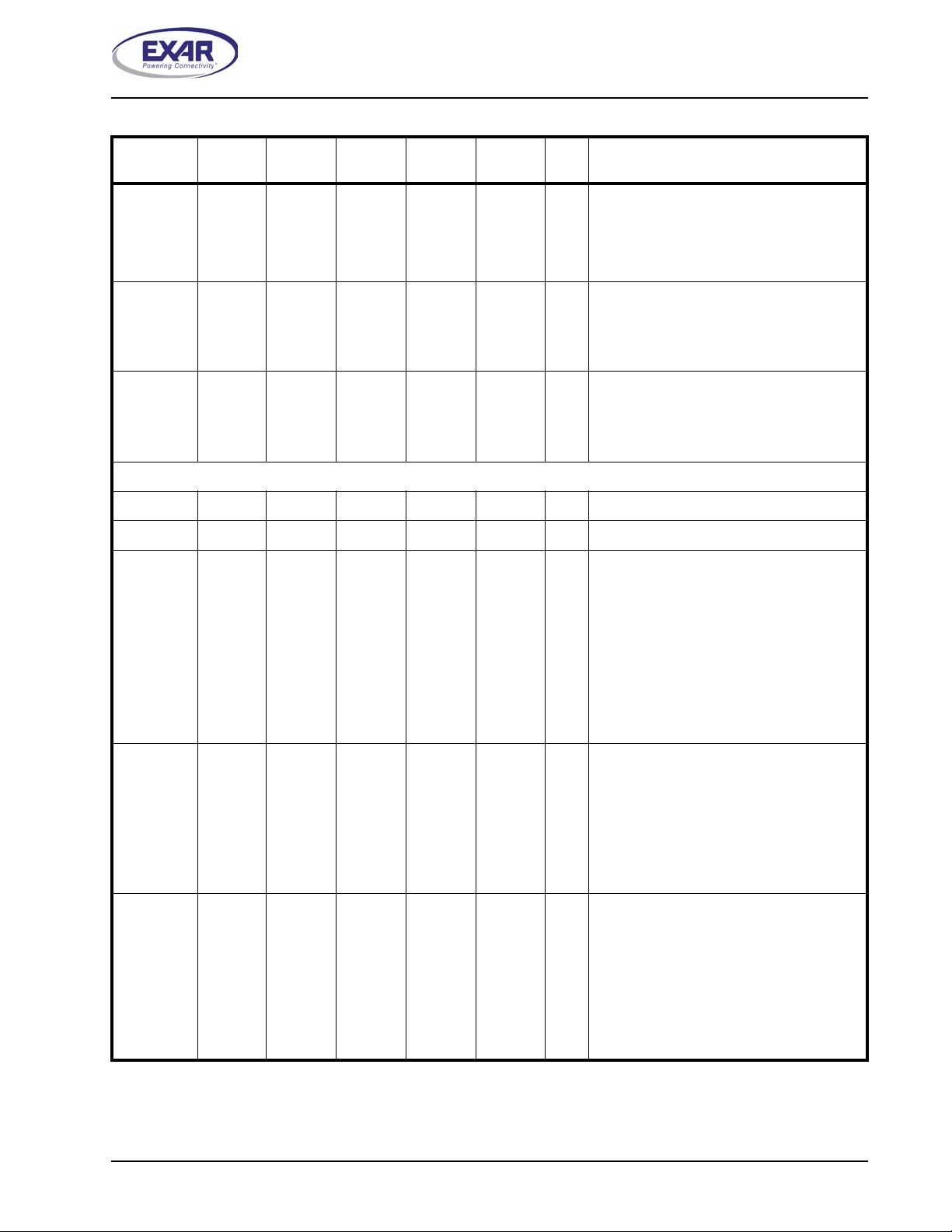
The XR16M6541 (M654) is an enhanced quad
Universal Asynchronous Receiver and Transmitter
(UART) each with 64 bytes of transmit and receive
FIFOs, programmable transmit and receive FIFO
trigger levels, automatic hardware and software flow
control, and data rates of up to 16 Mbps at 4X
sampling rate. Each UART has a set of registers that
provide the user with operating status and control,
receiver error indications, and modem serial interface
controls. An internal loopback capability allows
onboard diagnostics. The M654 is available in a 48pin QFN, 64-pin LQFP, 68-pin PLCC, 80-pin LQFP
and 100-pin QFP packages. The 64-pin and 80-pin
packages only offer the 16 mode interface, but the
48, 68 and 100 pin packages offer an additional 68
mode interface which allows easy integration with
Motorola processors. The XR16M654IV (64-pin)
offers three state interrupt output while the
XR16M654DIV provides continuous interrupt output.
The 100 pin package provides additional FIFO status
outputs (TXRDY# and RXRDY# A-D), separate
infrared transmit data outputs (IRTX A-D) and
channel C external clock input (CHCCLK). The
XR16M654 is compatible with the industry standard
ST16C554 and ST16C654/654D.
N
OTE
:
1 Covered by U.S. Patent #5,649,122.
FEATURES
•
Pin-to-pin compatible with ST16C454, ST16C554,
TI’s TL16C754B and NXP’s SC16C654B
•
Intel or Motorola Data Bus Interface select
•
Four independent UART channels
■
Register Set Compatible to 16C550
■
Data rates of up to 16 Mbps
■
64 Byte Transmit FIFO
■
64 Byte Receive FIFO with error tags
■
4 Selectable TX and RX FIFO Trigger Levels
■
Automatic Hardware (RTS/CTS) Flow Control
■
Automatic Software (Xon/Xoff) Flow Control
■
Progammable Xon/Xoff characters
■
Wireless Infrared (IrDA 1.0) Encoder/Decoder
■
Full modem interface
•
1.62V to 3.63V supply operation
•
Sleep Mode with automatic wake-up
•
Crystal oscillator or external clock input
APPLICATIONS
•
Portable Appliances
•
Telecommunication Network Routers
•
Ethernet Network Routers
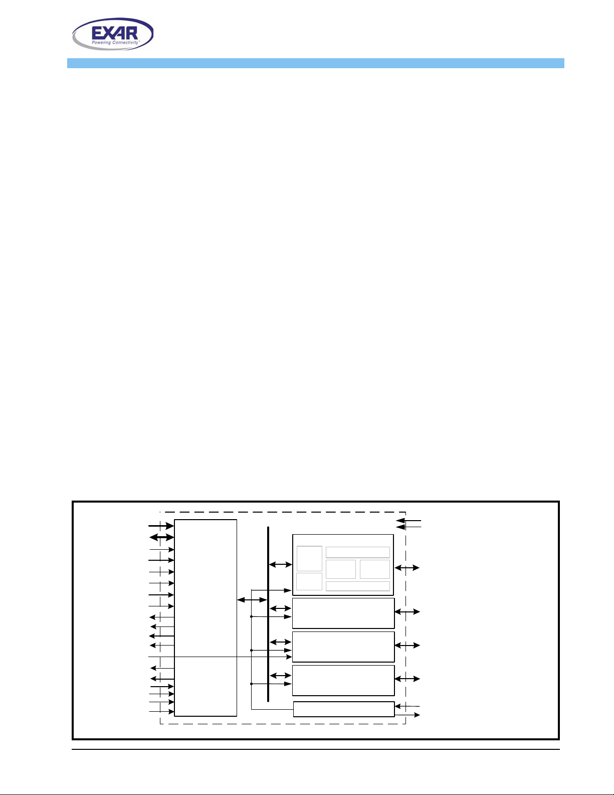
F
IGURE
1. XR16M654 B
A2:A0
D7:D0
IOR#
IOW#
CSA#
CSB#
CSC#
CSD#
INTA
INTB
INTC
INTD
CHCCLK
TXRDY# A-D
RXRDY# A-D
Reset
16/68#
INTSEL
CLKSEL
LOCK DIAGRAM
Data Bus
Interface
•
Cellular Data Devices
•
Factory Automation and Process Controls
UART Channel A
64 Byte TX FIFO
UART
Regs
TX & RX
BRG
64 Byte RX FIFO
UART Channel B
(same as Channel A)
UART Channel C
(same as Channel A)
UART Channel D
(same as Channel A)
Crystal Osc/Buffer
IR
ENDEC
1.62V to 3.6V VCC
GND
TXA, RXA, IR T XA, DTRA#,
DSRA#, RTSA#, CTSA#,
CDA#, RIA#
TXB, RXB, IR T XB, DTRB#,
DSRB#, RTSB#, CTSB#,
CDB#, RIB#
TXC, RXC, IRTXC, DTRC#,
DSRC#, RTSC#, CTSC#,
CDC#, RIC#
TXD, RXD, IRTXD, DTRD#,
DSRD#, RTSD#, CTSD#,
CDD#, RID#
XTAL1
XTAL2
654 BLK
Exar
Corporation 48720 Kato Road, Fremont CA, 94538 • (510) 668-7000 • FAX (510) 668-7017 • www.exar.com
Page 2
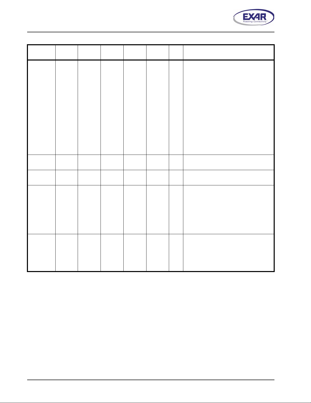
XR16M654/654D
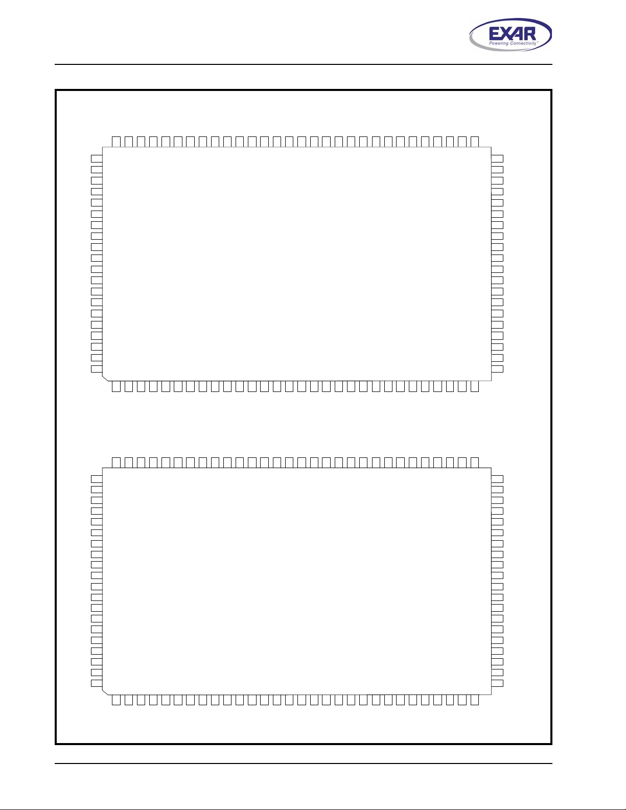
1.62V TO 3.63V QUAD UART WITH 64-BYTE FIFO
F
IGURE
2. PIN OUT A
TXRDYD#
81
RXRDYD#
82
CDD#
83
84
RID#
RXD
85
VCC
86
INTSEL
87
D0
88
89
D1
D2
90
D3
91
D4
92
D5
93
94
D6
95
D7
96
GND
97
RXA
98
RIA#
99
CDA#
100
RXRDYA#
N.C.
80
1
N.C.
SSIGNMENT FOR
N.C.
N.C.
N.C.
IRTXD
FSRS#
7978777675747372717069
2
3
4
5
6
N.C.
N.C.
N.C.
IRTXA
TXRDYA#
100-
PIN
DSRD#
CTSD#
DTRD#
GND
RTSD#
7
8
9
101112
VCC
CTSA#
DSRA#
RTSA#
DTRA#
QFP P
INTD
TXD
CSD#
686766656463626160
XR16M654
100-pin QFP
Intel Mode
Connect 16/68# pin to VCC
13141516171819202122232425
TXA
INTA
CSA#
ACKAGES IN
IOR#
TXC
INTC
CSC#
TXB
IOW#
INTB
CSB#
RTSC#
RTSB#
16
VCC
GND
AND
68 M
ODE
DSRC#
IRTXC
TXRDYC#
N.C.
DTRC#
CTSC#
595857565554535251
IRTXB
CTSB#
DSRB#
DTRB#
N.C.
2627282930
N.C.
N.C.
TXRDYB#
REV. 1.0.0
N.C.
N.C.
N.C.
RXRDYC#
50
49
CDC#
48
RIC#
47
RXC
GND
46
45
TXRDY#
RXRDY#
44
RESET
43
CHCCLK
42
XTAL2
41
XTAL1
40
A0
39
38
A1
37
A2
36
16/68#
35
CLKSEL
34
RXB
RIB#
33
CDB#
32
RXRDYB#
31
N.C.
N.C.
N.C.
TXRDYD#
RXRDYD#
CDD#
RID#
RXD
VCC
INTSEL
GND
RXA
RIA#
CDA#
RXRDYA#
N.C.
N.C.
N.C.
N.C.
IRTXD
DSRD#
CTSD#
FSRS#
80
7978777675747372717069
81
82
83
84
85
86
87
D0
88
89
D1
90
D2
91
D3
92
D4
93
D5
94
D6
95
D7
96
97
98
99
100
1
2
3
4
5
6
N.C.
N.C.
N.C.
N.C.
IRTXA
TXRDYA#
DTRD#
7
8
9
CTSA#
DSRA#
DTRA#
N.C.
N.C.
TXD
N.C.
GND
RTSD#
68
TXCA4N.C.
67666564636261
XR16M654
100-pin QFP
Motorola Mode
Connect 16/6 8# pi n to GND
101112
VCC
13
14151617181920
R/W#
A3
TXB
TXA
IRQ#
CSA#
RTSA#
VCC
RTSC#
N.C.
GND
RTSB#
DSRC#
CTSC#
59
CTSB#
IRTXC
585756
IRTXB
DSRB#
DTRC#
60
2122232425
DTRB#
TXRDYC#
N.C.
N.C.
5554535251
2627282930
N.C.
N.C.
TXRDYB#
N.C.
N.C.
N.C.
RXRDYC#
50
49
CDC#
48
RIC#
47
RXC
GND
46
45
TXRDY#
RXRDY#
44
RESET
43
CHCCLK
42
XTAL2
41
XTAL1
40
A0
39
38
A1
37
A2
36
16/68#
35
CLKSEL
34
RXB
RIB#
33
CDB#
32
RXRDYB#
31
N.C.
N.C.
N.C.
2
Page 3
XR16M654/654D
REV. 1.0.0
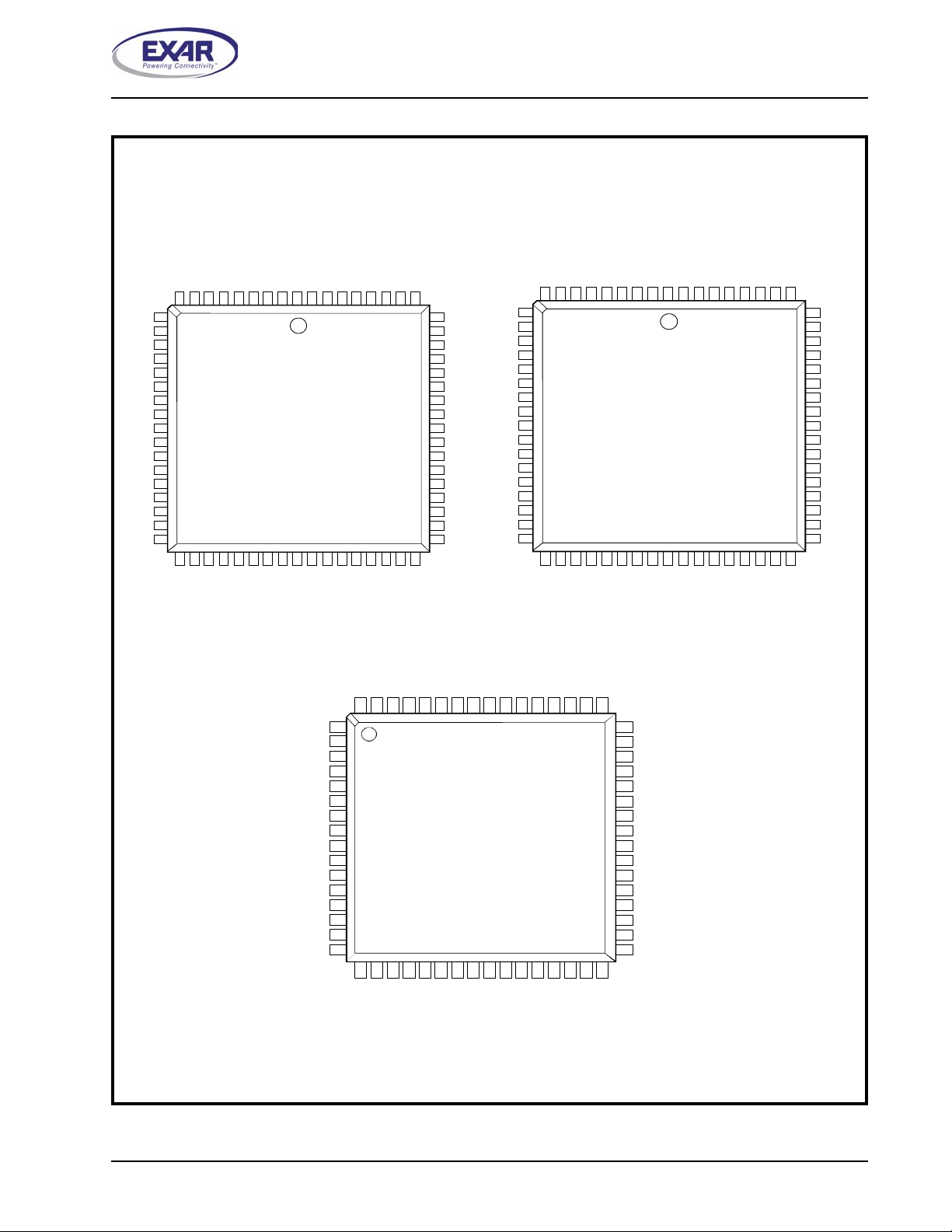
F
IGURE
10
DSRA#
11
CTSA#
12
DTRA#
13
VCC
14
RTSA#
15
INTA
16
CSA#
17
TXA
18
IOW#
19
TXB
20
CSB#
21
INTB
22
RTSB#
23
GND
24
DTRB#
25
CTSB#
26
DSRB#
3. PIN OUT A
CDA#
RIA#
987654321
SSIGNMENT FOR
GNDD7D6D5D4D3D2D1D0
RXA
68-
INTSEL
68676665646362
XR16M654
68-pin PLCC
Intel Mode
(16/68# pin connected to VCC)
2728293031323334353637383940414243
RIB#
CDB#
A2A1A0
RXB
16/68#
CLKSEL
XTAL1
XTAL2
RESET
TXRDY#
RXRDY#
VCC
GND
PIN
PLCC P
RXD
RID#
RXC
RIC#
1.62V TO 3.63V QUAD UART WITH 64-BYTE FIFO
ACKAGES IN
CDD#
63
60
59
58
57
56
55
54
53
52
51
50
49
48
47
46
45
44
CDC#
DSRD#
CTSD#
DTRD#
GND
RTSD#
INTD
CSD#
TXD
IOR#
TXC
CSC#
INTC
RTSC#
VCC
DTRC#
CTSC#
DSRC#
DSRA#
CTSA#
DTRA#
VCC
RTSA#
IRQ#
CS#
TXA
R/W#
TXB
N.C.
RTSB#
GND
DTRB#
CTSB#
DSRB#
16
AND
68 M
ODE AND
GNDD7D6D5D4D3D2D1D0
CDA#
RIA#
RXA
987654321
10
11
12
13
14
15
16
17
18
19
20
A3
21
22
23
24
25
26
(16/68# pin connected to GND)
2728293031323334353637383940414243
RXB
RIB#
CDB#
XR16M654
68-pin PLCC
Motorola Mode
A2A1A0
16/68#
CLKSEL
64-
68676665646362
XTAL1
XTAL2
RESET
RXRDY#
PIN
GND
TXRDY#
LQFP P
VCC
RXD
RID#
RXC
GND
RIC#
ACKAGES
CDD#
63
60
DSRD#
59
CTSD#
DTRD#
58
GND
57
RTSD#
56
55
N.C.
54
N.C.
TXD
53
N.C.
52
TXC
51
50
A4
49
N.C.
RTSC#
48
VCC
47
DTRC#
46
45
CTSC#
44
DSRC#
CDC#
DSRA#
CTSA#
DTRA#
VCC
RTSA#
INTA
CSA#
TXA
IOW#
TXB
CSB#
INTB
RTSB#
GND
DTRB#
CTSB#
RXA
D7
D6D5D4
CDA#
64
1
2
3
4
5
6
7
8
9
10
11
12
13
14
15
16
17
DSRB#
GND
RIA#
62
61605958575655
63
Intel M ode Only
21
20
18
19
RIB#
RXB
CDB#
CLKSEL
XR16M654
64-pin TQFP
22
A1
A2
D2
D1
D3
545352
23
252627
24
A0
XTAL1
XTAL2
RESET
RXD
VCC
D0
28
GND
RID#
CDD#
51
50
49
48
DSRD#
47
CTSD#
46
DTRD#
45
GND
44
RTSD#
43
INTD
42
CSD#
TXD
41
IOR#
40
TXC
39
38
CSC#
37
INTC
36
RTSC#
35
VCC
34
DTRC#
33
CTSC#
31
29
30
32
RXC
RIC#
CDC#
DSRC#
3
Page 4
XR16M654/654D
1.62V TO 3.63V QUAD UART WITH 64-BYTE FIFO
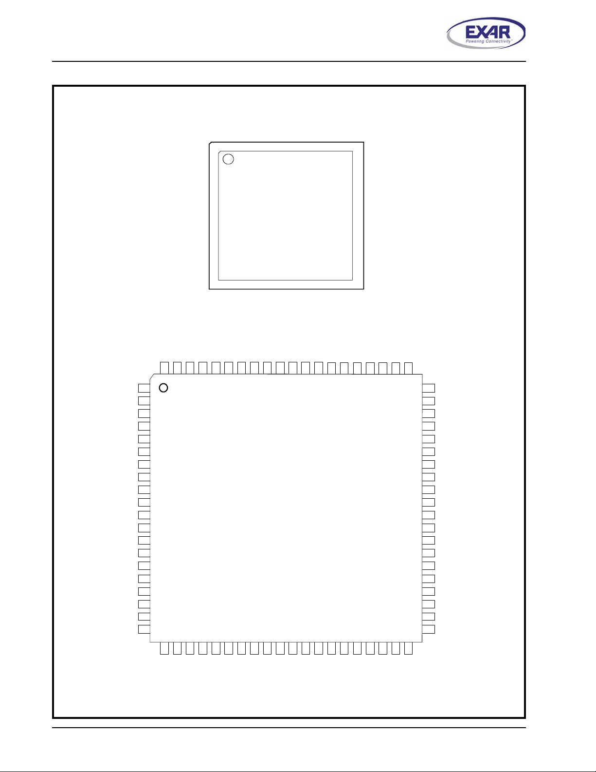
F
IGURE
4. PIN OUT A
SSIGNMENT FOR
CTSA#
VCC
RTSA#
INTA
CSA#
TXA
IOW#
TXB
CSB#
INTB
RTSB#
CTSB#
48-
PIN
RXA
GND
4847464544
1
2
3
4
5
6
7
8
9
10
11
12
13
141516
RXB
16/68#
QFN P
D7D6D5
A1
A2
XR16M654
48-pin QFN
17
ACKAGE AND
D4
D3
D2
434241
1819202122
A0
XTAL1
XTAL2
RESET
REV. 1.0.0
80-
PIN
LQFP P
D1
D0
VCC
INTSEL
40
38
37
39
RXC
GND
23
CTSC#
24
36
35
34
33
32
30
29
28
27
26
25
VCC
RXD
CTSD#
RTSD#
INTD
CSD#
31
TXD
CSC#
RTSC#
ACKAGE
GND
IOR#
TXC
INTC
NC
NC
DSRA#
CTSA#
DTRA#
VCC
RTSA#
INTA
CSA#
TXA
IOW#
TXB
CSB#
INTB
RTSB#
GND
DTRB#
CTSB#
DSRB#
D5
GND
N.C.
RIA#
CDA#
80
79
78
1
2
3
4
5
6
7
8
9
10
11
12
13
14
15
16
17
18
19
NC
20
D7
RXA
77
76
75
D4
D6
74
73
72
XR16M654
80-pin LQFP
Intel M ode on ly
D1
D2
D3
71
70
69
VCC
D0
INTSEL
RXD
RID#
68
67
66
65
64
N.C.
N.C.
CDD#
63
62
61
N.C.
60
DSRD#
59
58
CTSD#
DTRD#
57
56
GND
RTSD#
55
54
INTD
53
CSD#
TXD
52
51
IOR#
50
TXC
49
CSC#
INTC
48
RTSC#
47
VCC
46
45
DTRC#
CTSC#
44
DSRC#
43
N.C.
42
41
N.C.
21
22
23
24
25
26
27
28
293031
A2
N.C.
N.C.
RXB
RIB#
CDB#
CLKSEL
A1
N.C.
32
33
34
35
36
37
38
39
40
A0
XTAL1
XTAL2
RESET
GND
RXC
TXRDY#
RXRDY#
N.C.
RIC#
CDC#
4
Page 5
XR16M654/654D
REV. 1.0.0
ORDERING INFORMATION
P
ART NUMBER
XR16M654IJ68 68-Lead PLCC -40°C to +85°C Active
XR16M654IV64 64-Lead LQFP -40°C to +85°C Active
XR16M654DIV64 64-Lead LQFP -40°C to +85°C Active
XR16M654IQ100 100-Lea d QFP -40°C to +85°C Active
XR16M654IL48 48-pin QFN -40°C to +85°C Active
XR16M654IV80 80-Lead LQFP -40°C to +85°C Active
PIN DESCRIPTIONS
Pin Description
N
AME
48-QFN
PIN #
DATA BUS INTERFACE
A2
A1
A0
15
16
17
64-LQFP
PIN #
22
23
24
68-PLCC
PIN#
32
33
34
P
ACKAGE
80-LQFP
PIN #
28
29
30
1.62V TO 3.63V QUAD UART WITH 64-BYTE FIFO
O
100-QFP
PIN #
37
38
39
PERATING TEMPERATURE
R
ANGE
T
YPE
I Address data lines [2:0]. These 3 ad dress
lines select one of the internal registers in
UART channel A-D during a data bus trans
action.
D
ESCRIPTION
D
EVICE STATUS
-
D7
D6
D5
D4
D3
D2
D1
D0
IOR#
(VCC)
46
45
44
43
42
41
40
39
60
59
58
57
56
55
54
53
68
67
66
5
4
3
2
1
75
74
73
72
71
70
69
68
95
94
93
92
91
90
89
88
I/O Data bus lines [7:0] (bidirectional).
29 40 52 51 66 I When 16/68# pin is HIGH, the Intel bus
interface is selected and this input becomes
read strobe (active low). The falling edge
instigates an internal read cycle and
retrieves the data byte from an internal reg
ister pointed by the address lines [A2:A0],
puts the data byte on the data bus to allow
the host processor to read it on the rising
edge.
When 16/68# pin is LOW, the Motorola bus
interface is selected and this input is not
used and should be connected to VCC.
-
5
Page 6
XR16M654/654D
1.62V TO 3.63V QUAD UART WITH 64-BYTE FIFO
Pin Description
N
AME
IOW#
(R/W#)
CSA#
(CS#)
CSB#
(A3)
48-QFN
PIN #
64-LQFP
PIN #
7 9 18 11 15 I When 16/68# pin is HIGH, it selects Intel
5 7 16 9 13 I When 16/68# pin is HIGH, this input is chip
9 11 20 13 17 I When 16/68# pin is HIGH, this input is chip
68-PLCC
PIN#
80-LQFP
PIN #
100-QFP
PIN #
YPE
T
bus interface and this input becomes write
strobe (active low). The falling edge insti
gates the internal write cycle and the rising
edge transfers the data byte on the data
bus to an internal register pointed by the
address lines.
When 16/68# pin is LOW, the Motorola bus
interface is selected and this input becomes
read (logic 1) and write (logic 0) signal.
select A (active low) to enable channel A in
the device.
When 16/68# pin is LOW, this input
becomes the chip select (active low) for the
Motorola bus interface.
select B (active low) to enable channel B in
the device.
When 16/68# pin is LOW, this input
becomes address line A3 which is used for
channel selection in the Motorola bus inter
face.
D
ESCRIPTION
REV. 1.0.0
-
-
CSC#
(A4)
CSD#
(VCC)
INTA
(IRQ#)
27 38 50 49 64 I When 16/68# pin is HIGH, this input is chip
select C (active low) to enable channel C in
the device.
When 16/68# pin is LOW, this input
becomes address line A4 which is used for
channel selection in the Motorola bus inter
face.
31 42 54 53 68 I When 16/68# pin is HIGH, this input is chip
select D (active low) to enable channel D in
the device.
When 16/68# pin is LOW, this input is not
used and should be connected VCC.
4 6 15 8 12 O
When 16/68# pin is HIGH for Intel bus interface, this ouput becomes channel A inter-
(OD)
rupt output. The output state is defined by
the user and through the software setting of
MCR[3]. INTA is set to the active mode
when MCR[3] is set to a logic 1. INTA is set
to the three state mode when MCR[3] is set
to a logic 0 (default). See MCR[3].
When 16/68# pin is LOW for Motorola bus
interface, this output becomes device inter
rupt output (active low, open drain). An
external pull-up resistor is required for
proper operation.
-
-
6
Page 7
XR16M654/654D
REV. 1.0.0
1.62V TO 3.63V QUAD UART WITH 64-BYTE FIFO
Pin Description
N
AME
INTB
INTC
INTD
(N.C.)
INTSEL 38 - 65 67 87 I Interrupt Select (active high, input with
TXRDYA#
TXRDYB#
TXRDYC#
TXRDYD#
RXRDYA#
RXRDYB#
RXRDYC#
RXRDYD#
48-QFN
PIN #
10
26
32
-
-
-
-
-
-
-
-
64-LQFP
PIN #
12
37
43
-
-
-
-
-
-
-
-
68-PLCC
PIN#
21
49
55
-
-
-
-
-
-
-
-
80-LQFP
PIN #
14
48
54
-
-
-
-
-
-
-
-
100-QFP
PIN #
18
63
69
5
25
56
81
100
31
50
82
YPE
T
O When 16/68# pin is HIGH for Intel bus inter-
face, these ouputs become the interrupt
outputs for channels B, C, and D. The out
put state is defined by the user through the
software setting of MCR[3]. The interrupt
outputs are set to the active mode when
MCR[3] is set to a logic 1 and are set to the
three state mode when MCR[3] is set to a
logic 0 (default). See MCR[3].
When 16/68# pin is LOW for Motorola bus
interface, these outputs are unused and will
stay at logic zero level. Leave these out
puts unconnected.
internal pull-down).
When 16/68# pin is HIGH for Intel bus inter-
face, this pin can be used in conjunction
with MCR bit-3 to enable or disable the INT
A-D pins or override MCR bit-3 and enable
the interrupt outputs. Interrupt outputs are
enabled continuously when this pin is
HIGH. MCR bit-3 enables and disables the
interrupt output pins. In this mode, MCR
bit-3 is set to a logic 1 to enable the continu
ous output. See MCR bit-3 description for
full detail. This pin must be LOW in the
Motorola bus interface mode. For the 64
pin packages, this pin is bonded to VCC
internally in the XR16M654D so the INT
outputs operate in the continuous interrupt
mode. This pin is bonded to GND internally
in the XR16M654 and therefore requires
setting MCR bit-3 for enabling the interrupt
output pins.
UART channels A-D Transmitter Ready
O
(active low). The outputs provide the TX
FIFO/THR status for transmit channels A-D.
Table 5. If these outputs are unused,
See
leave them unconnected.
O UART channels A-D Receiver Ready
(active low). This output provides the RX
FIFO/RHR status for receive channels A-D.
Table 5. If these outputs are unused,
See
leave them unconnected.
D
ESCRIPTION
-
-
-
TXRDY# - - 39 35 45 O T ransmitter Ready (active low). This output
is a logically ANDed status of TXRDY# AD. See
leave it unconnected.
RXRDY# - - 38 34 44 O Receiver Ready (active low). This output is
a logically ANDed status of RXRDY# A-D.
See
it unconnected.
Table 5. If this output is unused,
Table 5. If this output is unused, leave
7
Page 8
XR16M654/654D
1.62V TO 3.63V QUAD UART WITH 64-BYTE FIFO
Pin Description
N
AME
FSRS# - - - - 76 I FIFO Status Register Select (active low
MODEM OR SERIAL I/O INTERFACE
TXA
TXB
TXC
TXD
48-QFN
PIN #
28
30
6
8
64-LQFP
PIN #
8
10
39
41
68-PLCC
PIN#
17
19
51
53
80-LQFP
PIN #
10
12
50
52
100-QFP
PIN #
14
16
65
67
YPE
T
input with internal pull-up).
The content of the FSTAT register is placed
on the data bus when this pin becomes
active. However it should be noted, D0-D3
contain the inverted logic st ates of TXRDY#
A-D pins, and D4-D7 the logic states (uninverted) of RXRDY# A-D pins. A valid
address is not required when reading this
status register.
O UART channels A-D Transmit Data and
infrared transmit data. Standard transmit
and receive interface is enabled when
MCR[6] = 0. In this mode, the TX signal will
be a logic 1 during reset, or idle (no data).
Infrared IrDA transmit and receive interface
is enabled when MCR[6] = 1. In the Infra
red mode, the inactive state (no data) for
the Infrared encoder/decoder interface is a
logic 0.
D
ESCRIPTION
REV. 1.0.0
-
IRTXA
IRTXB
IRTXC
IRTXD
RXA
RXB
RXC
RXD
RTSA#
RTSB#
RTSC#
RTSD#
CTSA#
CTSB#
CTSC#
CTSD#
DTRA#
DTRB#
DTRC#
DTRD#
48
13
22
36
11
25
33
12
23
35
-
-
-
-
3
1
-
-
-
-
62
20
29
51
13
36
44
16
33
47
15
34
46
-
-
-
-
5
2
3
29
41
63
14
22
48
56
11
25
45
59
12
24
46
58
-
-
-
-
7
77
25
37
65
15
47
55
18
44
58
17
45
57
-
-
-
-
7
4
5
24
57
75
97
34
47
85
11
19
62
70
22
59
73
21
60
72
6
8
9
O UART channel A-D Infrared Transmit Data.
The inactive state (no data) for the Infrared
encoder/decoder interface is LOW.
Regardless of the logic state of MCR bit-6,
this pin will be operating in the Infrared
mode.
I UART channel A-D Receive Data or infra-
red receive data. Normal receive data input
must idle HIGH.
O UART channels A-D Request-to-Send
(active low) or general purpose output. This
output must be asserted prior to using auto
RTS flow control, see EFR[6], MCR[1], and
IER[6]. Also see
puts are not used, leave them unconnected.
I UART channels A-D Clear-to-Send (active
low) or general purpose input. It can be
used for auto CTS flow control, see EFR[7],
and IER[7]. Also see
inputs should be connected to VCC when
not used.
O UART channels A-D Data-Terminal-Ready
(active low) or general purpose output. If
these outputs are not used, leave them
unconnected.
Figure 12
. If these out-
Figure 12
. These
8
Page 9
XR16M654/654D
REV. 1.0.0
1.62V TO 3.63V QUAD UART WITH 64-BYTE FIFO
Pin Description
N
AME
DSRA#
DSRB#
DSRC#
DSRD#
CDA#
CDB#
CDC#
CDD#
RIA#
RIB#
RIC#
RID#
ANCILLARY SIGNALS
XTAL1 18 25 35 31 40 I Crystal or external clock input.
XTAL2 19 26 36 32 41 O Crystal or buffered clock output.
48-QFN
PIN #
-
-
-
-
-
-
-
-
-
-
-
-
64-LQFP
PIN #
1
17
32
48
64
18
31
49
63
19
30
50
68-PLCC
PIN#
10
26
44
60
9
27
43
61
8
28
42
62
80-LQFP
PIN #
3
19
43
59
79
23
39
63
78
24
38
64
100-QFP
PIN #
7
23
58
74
99
32
49
83
98
33
48
84
YPE
T
I UART channels A-D Data-Set-Ready
(active low) or general purpose input. This
input should be connected to VCC when
not used. This input has no effect on the
UART.
I UART channels A-D Carrier-Detect (active
low) or general purpose input. This input
should be connected to VCC when not
used. This input has no effect on the UART.
I UART channels A-D Ring-Indicator (active
low) or general purpose input. This input
should be connected to VCC when not
used. This input has no effect on the UART.
D
ESCRIPTION
16/68# 14 - 31 - 36 I Intel or Motorola Bus Select (input with
internal pull-up).
When 16/68# pin is HIGH, 16 or Intel Mode,
the device will operate in the Intel bus type
of interface.
When 16/68# pin is LOW, 68 or Motorola
mode, the device will operate in the Motorola bus type of interface.
Motorola bus interface is not available on
the 64 pin package.
CLKSEL - 21 30 26 35 I Baud-Rate-Generator Input Clock Pres -
caler Select for channels A-D. This input is
only sampled during power up or a reset.
Connect to VCC for divide by 1 (default)
and GND for divide by 4. MCR[7] can over
ride the state of this pin following a reset or
initialization. See MCR bit-7 and
in the Baud Rate Generator section.
CHCCLK - - - - 42 I This input provides the clock for UART
channel C. An external 16X baud clock or
the crystal oscillator’s output, XTAL2, must
be connected to this pin for normal opera
tion. This input may also be used with MIDI
(Musical Instrument Digital Interface) appli
cations when an external MIDI clock is provided. This pin is only available in the 100pin QFP package.
Figure 7
-
-
-
9
Page 10
XR16M654/654D
1.62V TO 3.63V QUAD UART WITH 64-BYTE FIFO
Pin Description
N
AME
RESET
(RESET#)
VCC 2, 24, 37 4, 35, 52 13, 47, 646, 46, 66 10, 61, 86Pwr 1.62V to 3.63V power supply.
GND 21, 47 14, 28,
48-QFN
PIN #
20 27 37 33 43 I When 16/68# pin is HIGH for Intel bus inter-
64-LQFP
PIN #
45, 61
68-PLCC
PIN#
6, 23, 40, 5716, 36,
80-LQFP
PIN #
56, 76
100-QFP
PIN #
20, 46,
71, 96
YPE
T
face, this input becomes the Reset pin
(active high). In this case, a 40 ns mini
mum HIGH pulse on this pin will reset the
internal registers and all outputs. The UART
transmitter output will be held HIGH, the
receiver input will be ignored and outputs
are reset during reset period (
When 16/68# pin is at LOW for Motorola
bus interface, this input becomes Reset#
pin (active low). This pin functions similarly,
but instead of a HIGH pulse, a 40 ns mini
mum LOW pulse will reset the internal registers and outputs.
Motorola bus interface is not available on
the 64 pin package.
Pwr Power supply common, ground.
D
ESCRIPTION
REV. 1.0.0
-
Table 17).
-
GND Center
Pad
N.C. - - - 1, 2, 20,
Pin type: I=Input, O=Output, I/O= Input/output, OD=Output Open Drain.
N/A N/A N/A N/A
21, 22,
27, 40,
41, 42,
60, 61,
62, 80
Pwr The center pad on the backside of the QFN
package is metallic and should be connected to GND on the PCB. The thermal
pad size on the PCB should be the approximate size of this center pad and should be
solder mask defined. The solder mask
opening should be at least 0.0025" inwards
from the edge of the PCB thermal pad.
No Connection. These pins are not used in
either the Intel or Motorola bus modes.
10
Page 11

XR16M654/654D
REV. 1.0.0
1.0 PRODUCT DESCRIPTION
The XR16M654 (M654) integrates the functions of 4 enhanced 16C550 Universal Asynchrounous Receiver
and Transmitter (UART). Each UART is independently controlled and has its own set of device configuration
registers. The configuration registers set is 16550 UART compatible for control, status and data transfer.
Additionally, each UART channel has 64 bytes of transmit and receive FIFOs, autom atic RTS/CTS hardware
flow control, automatic Xon/Xoff and special character software flow control, infrared encoder and decoder
(IrDA ver 1.0), programmable fractional baud rate generator with a prescaler of divide by 1 or 4, and data rate
up to 16 Mbps. The XR16M654 can operate from 1.62 to 3.63 volts. The M654 is fabricated with an advanced
CMOS process.
Enhanced FIFO
The M654 QUART provides a solution that supports 64 bytes of transmit and receive FIFO memory, instead of
16 bytes in the ST16C554, or one byte in th e ST16C45 4. The M6 54 is d esigned to wor k with high perf orman ce
data communication systems, that require fast data processing time. Increased performance is realized in the
M654 by the larger transmit and receive FIFOs, FIFO trigger level control and automatic flow control
mechanism. This allows the external processor to handle more networking tasks within a given time. For
example, the ST16C554 with a 16 by te F IFO, unloads 16 bytes of receive data in 1.53 ms (This example uses
a character length of 11 bits, including start/stop bits at 115.2Kbps). This means the external CPU will have to
service the receive FIFO at 1.53 ms intervals. However with the 64 byte FIFO in the M654, the data buffer will
not require unloading/loading for 6.1 ms. This increases the service interval giving the external CPU additional
time for other applications and reducing the overall UART interrupt servicing time. In addition, the
programmable FIFO level trigger interrupt and automatic hardware/software flow control is uniquely provided
for maximum data throughput performance especially when operating in a multi-channel system. The
combination of the above greatly reduces the CPU’s bandwidth requirement, increases performance, and
reduces power consumption.
1.62V TO 3.63V QUAD UART WITH 64-BYTE FIFO
Data Rate
The M654 is capable of operation up to 16 Mbps at 3.3V with 4Xinternal sampling clock rate. The device can
operate at 3.3V with a crystal oscillator of up to 24 MHz crystal on pins XTAL1 and XTAL2, or external clock
source of 64 MHz on XTAL1 pin. With a typical crystal of 14.74 56 MHz and throu gh a software option, the user
can set the prescaler bit and sampling rate for data rates of up to 3.68 Mbps.
Enhanced Features
The rich feature set of the M654 is available through the internal registers. Automatic hardware/software flow
control, selectable transmit and receive FIFO trigger levels, selectable baud rates, infrared encoder/decoder
interface, modem interface controls, and a sleep mode are all standard features. MCR bit-5 provides a facility
for turning off (Xon) software flow control with any incoming (RX) character. In the 16 mode INTSEL and MCR
bit-3 can be configured to provide a software controlled or continuous interrupt capability. For backward
compatibility to the ST16C654, the 64-pin LQFP does not have the INTSEL pin. Instead, two different LQFP
packages are offered. The XR16M654DIV operates in the continuous interrupt enable mode by internally
bonding INTSEL to VCC. The XR16M654IV operates in conjunction with MCR bit-3 by internally bonding
INTSEL to GND.
The XR16M654 offers a clock prescaler select pin to allow system/board designers to preset the default baud
rate table on power up. The CL KSEL pin sel ect s t he div-b y-1 or d iv- by-4 pr escaler for the baud r ate ge nerato r.
It can then be overridden following initialization by MCR bit-7.
The 100 pin packages offer several other enhanced features. These features include a CHCCLK clock input,
FSTAT register and separate IrDA TX outputs.
operation or to external MIDI (Music Instrument Digital Interface) oscillator for MIDI applications. A separate
register (FSTAT) is provided for monitoring the real time status of the FIFO signals TXRDY# and RXRDY# for
each of the four UART channels (A-D). This reduces polling time involved in accessing individual channels.
The 100 pin QFP package also offers four separate IrDA (Infrared Data Association Standard) TX outputs for
Infrared applications. These outputs are provided in addition to the standard asynchronous modem data
outputs.
The CHCCLK must be connected to the XTAL2 pin for normal
11
Page 12
XR16M654/654D
1.62V TO 3.63V QUAD UART WITH 64-BYTE FIFO
REV. 1.0.0
2.0 FUNCTIONAL DESCRIPTIONS
2.1 CPU Interface
The CPU interface is 8 data bits wide with 3 ad dress lines and control signals to execute data bus read and
write transactions. The M654 data inter face support s the Inte l comp atible types of CPUs an d it is compat ible to
the industry standard 16C550 UART. No clock (oscillator nor external clock) is required for a data bus
transaction. Each bus cycle is asynchronous using CS# A-D, I OR# and IOW# or CS# , R/W#, A4 and A3 input s.
All four UART channels share the same data bus for host operations. A typical data bus interconnection for
Intel and Motorola mode is shown in
F
IGURE
5. XR16M654 T
UART_CSA#
UART_CSB#
UART_CSC#
UART_CSD#
UART_INTA
UART_INTB
UART_INTC
UART_INTD
UART_RESET RESET
YPICAL INTEL/MOTOROLA DATA BUS INTERCONNECTIONS
D0
D1
D2
D3
D4
D5
D6
D7
A0
A1
A2
IOR#
IOW#
VCC 16/68#
Figure 5.
D0
D1
D2
D3
D4
D5
D6
D7
A0
A1
A2
IOR#
IOW#
CSA#
CSB#
CSC#
CSD#
INTA
INTB
INTC
INTD
UART
Channel A
UART
Channel B
UART
Channel C
UART
Channel D
VCC
TXA
RXA
DTRA#
RTSA#
CTSA#
DSRA#
CDA#
RIA#
Similar
to Ch A
Similar
to Ch A
Similar
to Ch A
GND
VCC
Serial Interface of
RS-232
Serial Interface of
RS-232
Intel Data Bus (16 Mode) Interconnections
D0
D1
D2
D3
D4
D5
D6
D7
A0
A1
A2
A3
A4 CSC#
R/W#
UART_CS#
UART_IRQ#
UART_RESET#
VCC
(no connect)
(no connect)
(no connect)
Motorola Data Bus (68 Mode) Intercon nection s
VCC
VCC
D0
D1
D2
D3
D4
D5
D6
D7
A0
A1
A2
CSB#
CSD#
IOR#
IOW#
CSA#
INTA
INTB
INTC
INTD
RESET#
16/68#
UART
Channel A
UART
Channel B
UART
Channel C
UART
Channel D
VCC
TXA
RXA
DTRA#
RTSA#
CTSA#
DSRA#
CDA#
RIA#
Similar
to Ch A
Similar
to Ch A
Similar
to Ch A
GND
VCC
Serial Interface of
RS-232
Serial Interface of
RS-232
12
Page 13
XR16M654/654D
REV. 1.0.0
1.62V TO 3.63V QUAD UART WITH 64-BYTE FIFO
2.2 Device Reset
The RESET input resets the internal registers and the serial interface outputs in both channels to their default
state (see
Table 17). An active high pulse of longer than 40 ns duration will be required to activate the reset
function in the device. Following a power-on reset or an external reset, the M654 is software compatible with
previous generation of UARTs, 16C454 and 16C554.
2.3 Channel Selection
The UART provides the user with the capability to bi-directionally transfer information between an external
CPU and an external serial communication device. During Intel Bus Mode (16/68# pin is connected to VCC), a
logic 0 on chip select pins, CSA#, CSB#, CSC# or CSD# allows the user to select UART channel A, B, C or D
to configure, send transmit data and/or unload receive data to/from the UART. Selecting all four UARTs can be
useful during power up initialization to write to the same internal registers, but do not attempt to read from all
four uarts simultaneously. Individual channel select functions are shown in
T
ABLE
1: C
HANNEL
CSA# CSB# CSC# CSD# F
1 1 1 1 UART de-selected
0 1 1 1 Channel A selected
1 0 1 1 Channel B selected
A-D S
ELECT IN
16 M
UNCTION
Table 1.
ODE
1 1 0 1 Channel C selected
1 1 1 0 Channel D selected
0 0 0 0 Channels A-D selected
During Motorola Bus Mode (16/68# pin is connected to GND), the package interface pins are configured for
connection with Motorola, and other popular microprocessor bus types. In this mode the M654 decodes two
additional addresses, A3 and A4, to select one of the four UART ports. The A3 and A4 address decode
function is used only when in the Motorola Bus Mode.
T
ABLE
2: C
HANNEL
CS# A4 A3 F
1 X X UART de-selected
0 0 0 Channel A selected
0 0 1 Channel B selected
0 1 0 Channel C selected
0 1 1 Channel D selected
See Table 2.
A-D S
ELECT IN
68 M
UNCTION
ODE
13
Page 14
XR16M654/654D
1.62V TO 3.63V QUAD UART WITH 64-BYTE FIFO
REV. 1.0.0
2.4 Channels A-D Internal Registers
Each UART channel in the M654 has a set of enhanced registers for controlling, monitoring and data loading
and unloading. The configuration register set is compatible to those already available in the standard single
16C550. These registers function as data holding registers (THR/RHR), interrupt status an d control registers
(ISR/IER), a FIFO control register (FCR), receive line status and control registers (LSR/LCR), modem status
and control registers (MSR/MCR), programmable data rate (clock) divisor registers (DLL/DLM/DLD), and a
user accessible scratchpad register (SPR).
Beyond the general 16C550 features and capabilities, the M654 offers enhanced feature registers (EFR, Xon/
Xoff 1, Xon/Xoff 2, FSTAT) that provide automatic RTS and CTS hardware flow control and automatic Xon/Xoff
software flow control. All the register functions are discussed in full detail later in
“Section 3.0, UART
INTERNAL REGISTERS” on page 26.
2.5 INT Ouputs for Channels A-D
The interrupt outputs change according to the operating mode and enhanced features setup. Table 3 and 4
summarize the operating behavior for the transmitter and receiver. Also see Figure 21 through 26.
T
ABLE
3: INT PIN O
FCR BIT-0 = 0
(FIFO D
ISABLED
)
PERATION FOR TRANSMITTER FOR CHANNELS
FCR BIT-0 = 1 (FIFO E
FCR Bit-3 = 0
(DMA Mode Disabled)
NABLED
A-D
)
FCR Bit-3 = 1
(DMA Mode Enabled)
INT Pin LOW = a byte in THR
HIGH = THR empty
T
ABLE
4: INT PIN O
FCR BIT-0 = 0
(FIFO D
INT Pin LOW = no data
HIGH = 1 byte
ISABLED
LOW = FIFO above trigger level
HIGH = FIFO below trigger level or
FIFO empty
PERATION FOR RECEIVER FOR CHANNELS
)
FCR Bit-3 = 0
(DMA Mode Disabled)
LOW = FIFO below trigger level
HIGH = FIFO above trigger level
LOW = FIFO above trigger level
HIGH = FIFO below trigger level or
FIFO empty
FCR BIT-0 = 1 (FIFO E
LOW = FIFO below trigger level
HIGH = FIFO above trigger level
A-D
NABLED
)
FCR Bit-3 = 1
(DMA Mode Enabled)
2.6 DMA Mode
The device does not support direct memory access. The DMA Mode (a legacy term) in this document do es not
mean “direct memory access” but refers to data block transfer operation. The DMA mode affects the state of
the RXRDY# A-D and TXRDY# A-D output pins. The transmit and receive FIFO trigger levels provide
additional flexibility to the user for block mode operation. The LSR bits 5-6 provide an indication when the
transmitter is empty or has an empty location(s) for more data. The user can optionally operate the transmit
and receive FIFO in the DMA mode (FCR bit-3 = 1). When the transmit an d receive FIF Os are enabled and the
DMA mode is disabled (FCR bit-3 = 0), the M654 is placed in single-character mode for data transmit or
receive operation. When DMA mode is enabled (FCR bit-3 = 1), the user takes advantage of block mode
14
Page 15
XR16M654/654D
REV. 1.0.0
1.62V TO 3.63V QUAD UART WITH 64-BYTE FIFO
operation by loading or unloading the FIFO in a block sequence determined by the programmed trigger level.
The following table show their behavior. Also see
T
ABLE
5: TXRDY#
FCR
P
INS
RXRDY# LOW = 1 byte
HIGH = no data
TXRDY# LO W = THR empty
HIGH = byte in THR
BIT
(FIFO D
-0=0
ISABLED
AND
RXRDY# O
)
(DMA M
LOW = at least 1 byte in FIFO
HIGH = FIFO empty
LOW = FIFO empty
HIGH = at least 1 byte in FIFO
Figure 21 through 26.
UTPUTS IN
FCR BIT-3 = 0
ODE DISABLED
FIFO
AND
DMA M
FCR BIT-0=1 (FIFO E
)
HIGH to LOW transition when FIFO reaches the
trigger level, or timeout occurs
LOW to HIGH transition when FIFO empties
LOW = FIFO has at least 1 empty location
HIGH = FIFO is full
ODE FOR CHANNELS
NABLED
FCR BIT-3 = 1
(DMA M
ODE ENABLED
A-D
)
)
2.7 Crystal Oscillator or External Clock Input
The M654 includes an on-chip oscillator (XTAL1 and XTAL2) to produce a clock for both UART sections in the
device.
The CPU data bus does not require this clock for bus operation. The crystal oscillator provides a
system clock to the Baud Rate Generators (BRG) section found in each of the UART. XTAL1 is the input to the
oscillator or external clock buffer input with XTAL2 pin being the output. For programming details, see
“Section 2.8, Programmable Baud Rate Generator with Fractional Divisor” on page 15.
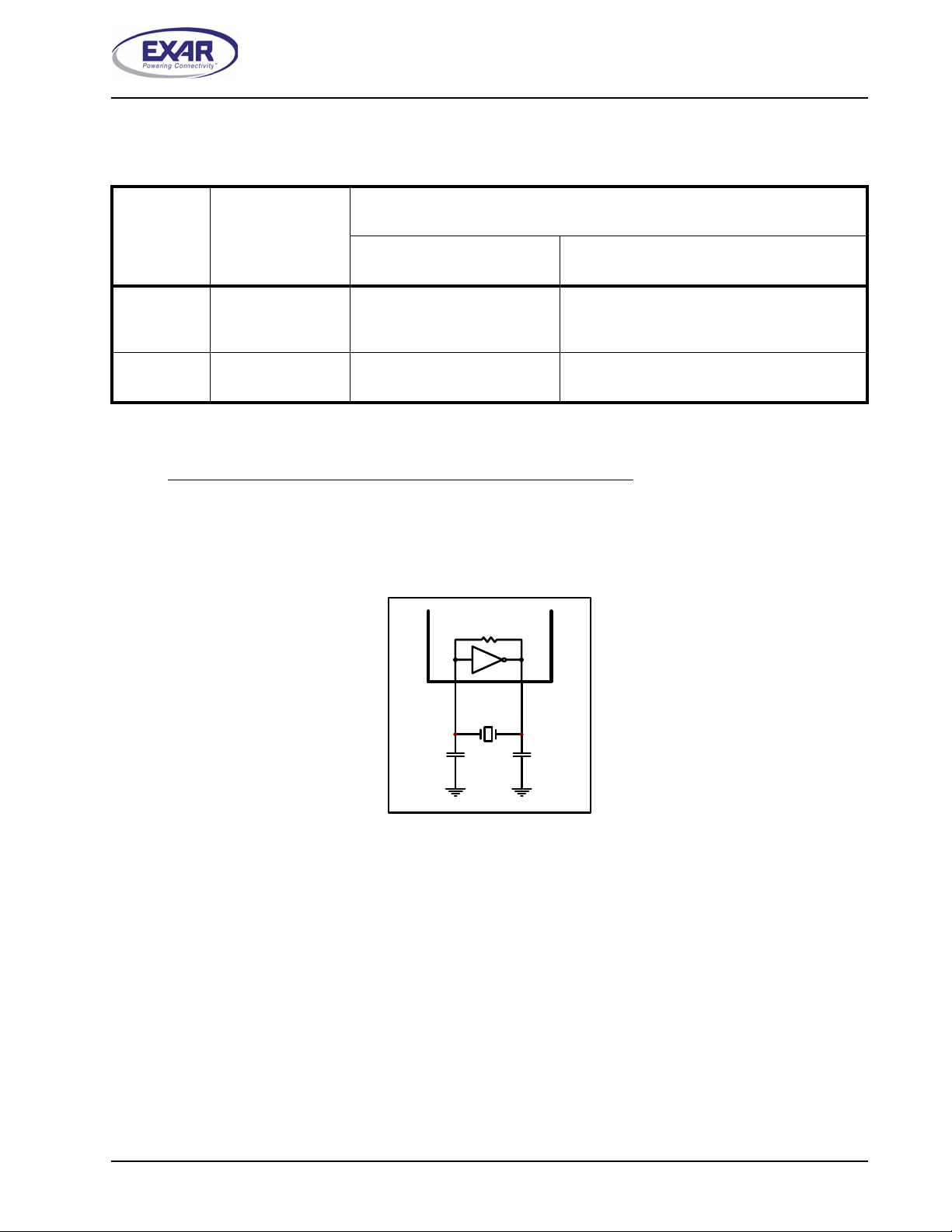
F
IGURE
6. T
YPICAL CRYSTAL CONNECTIONS
R=300K to 400K
XTAL1
C1
22-47pF
14.7456
MHz
XTAL2
C2
22-47pF
The on-chip oscillator is designed to use an industry standard microprocessor crystal (parallel resonant,
fundamental frequency with 10-22 pF capacitance load, ESR of 20-120 ohms and 100ppm frequency
tolerance) connected externally between the XTAL1 and XTAL2 pins. Typical oscillator connections are shown
in
Figure 6. Alternatively, an external clock can be connected to the XTAL1 pin to clock the internal baud rate
generator for standard or custom rates. For further reading on oscillator circuit please see application note
DAN108 on EXAR’s web site.
2.8 Programmable Baud Rate Generator with Fractional Divisor
Each UART has its own Baud Rate Generator (BRG) with a prescaler for the transmitter and receiver. The
prescaler is controlled by a software bit in the MCR register. The MCR register bit-7 sets the prescaler to divide
the input crystal or external clock by 1 or 4. The output of the prescaler clocks to the BRG. The BRG further
divides this clock by a programmable divisor between 1 and (2
16
- 0.0625) in increments of 0.0625 (1/16) to
obtain a 16X or 8X or 4X sampling clock of the serial data rate. The sampling clock is used by the transmitter
for data bit shifting and receiver for data sampling. The BRG divisor (DLL, DLM an d DLD register s) defaul ts to
the value of ’1’ (DLL = 0x01, DLM = 0x00 and DLD = 0x00) upon reset. Therefore, the BRG must be
15
Page 16
XR16M654/654D
1.62V TO 3.63V QUAD UART WITH 64-BYTE FIFO
REV. 1.0.0
programmed during initialization to the oper ating dat a rate. Th e DLL and DLM regi sters pr ovide the integer pa rt
of the divisor and the DLD register provides the fraction al p ar t of t he diviso r. Only the four lower bits of the DLD
are implemented and they are used to select a value from 0 (for setting 0000) to 0.9375 or 15/16 (for setting
1111). Programming the Baud Rate Generator Registers DLL, DLM and DLD provides the capability for
selecting the operating data rate.
Table 6 shows the standar d data rates available with a 24MHz crystal or
external clock at 16X clock rat e. If the pre-scaler is used (MCR bit-7 = 1), the output da ta rate will be 4 times
less than that shown in
Table 6. At 8X sampling rate, these data rates would double. And at 4X sampling rate,
they would quadruple. Also, when using 8X sampling mod e, please not e that the bit-t ime will have a jitt er (+/- 1/
16) whenever the DLD is non-zero and is an odd number. When using a non-standard data rate crystal or
external clock, the divisor value can be calculat ed with th e fo llo win g equ at ion (s ):
Required Divisor (decimal)=(XTAL1 clock frequency / prescaler) /(serial data rate x 16), with 16X mode, DLD[5:4]=’00’
Required Divisor (decimal)= (XTAL1 clock frequency / prescaler / (serial data rate x 8), with 8X mode, DLD[5:4] = ’01’
Required Divisor (decimal)= (XTAL1 clock frequency / prescaler / (serial data rate x 4), with 4X mode, DLD[5:4] = ’10’
The closest divisor that is obtainable in the M654 can be calculated using the following formula:
ROUND( (Required Divisor - TRUNC(Required Divisor) )*16)/16 + TRUNC(Required Divisor), where
DLM = TRUNC(Required Divisor) >> 8
DLL = TRUNC(Required Divisor) & 0xFF
DLD = ROUND( (Required Divisor-TRUNC(Required Divisor) )*16)
In the formulas above, please note that:
TRUNC (N) = Integer Part of N. For example, TRUNC (5.6) = 5.
ROUND (N) = N rounded towards the closest integer. For example, ROUND (7.3) = 7 and ROUND (9.9) = 10.
A >> B indicates right shifting the value ’A’ by ’B’ number of bits. For example, 0x78A3 >> 8 = 0x0078.
F
IGURE
7. B
AUD RATE GENERATOR
To Other
Channels
DLL, DLM and DLD
Registers
MCR Bit-7=0
(default)
Fractional Baud
Rate Generator
MCR Bit-7=1
Logic
16X or 8X or 4X
Sampling
Rate Clock
to Transmitter
and Receiver
XTAL1
XTAL2
Prescaler
Divide by 1
Crystal
Osc/
Buffer
Prescaler
Divide by 4
16
Page 17
XR16M654/654D
REV. 1.0.0
T
ABLE
6: T
YPICAL DATA RATES WITH A
Required
Output Data
Rate
400 3750 3750 E A6 0 0
2400 625 625 2 71 0 0
4800 312.5 312 8/16 1 38 8 0
9600 156.25 156 4/16 0 9C 4 0
10000 150 150 0 96 0 0
19200 78.125 78 2/16 0 4E 2 0
25000 60 60 0 3C 0 0
28800 52.0833 52 1/16 0 34 1 0.04
38400 39.0625 39 1/16 0 27 1 0
50000 30 30 0 1E 0 0
57600 26.0417 26 1/16 0 1A 1 0.08
75000 20 20 0 14 0 0
100000 15 15 0 F 0 0
115200 13.0208 13 0 D 0 0.16
153600 9.7656 9 12/16 0 9 C 0.16
200000 7.5 7 8/16 0 7 8 0
225000 6.6667 6 11/16 0 6 B 0.31
230400 6.5104 6 8/16 0 6 8 0.16
250000 6 6 0 6 0 0
300000 5 5 0 5 0 0
400000 3.75 3 12/16 0 3 C 0
460800 3.2552 3 4/16 0 3 4 0.16
500000 3 3 0 3 0 0
750000 2 2 0 2 0 0
921600 1.6276 1 10/16 0 1 A 0.16
1000000 1.5 1 8/16 0 1 8 0
D
IVISOR FOR
16x Clock
(Decimal)
O
D
BTAINABLE IN
M654
IVISOR
24 MHZ
DLM P
1.62V TO 3.63V QUAD UART WITH 64-BYTE FIFO
CRYSTAL OR EXTERNAL CLOCK AT
ALUE
V
ROGRAM
(HEX)
DLL P
ALUE
V
ROGRAM
(HEX)
DLD P
ALUE
V
16X S
ROGRAM
(HEX)
AMPLING
D
ATA ERROR
ATE
R
(%)
2.9 Transmitter
The transmitter section comprises of an 8-bit Transmit Shift Register (TSR) and 64 bytes of FIFO which
includes a byte-wide Transmit Holding Register (THR). TSR shifts out every data bit with the 16X/8X/4X
internal clock. A bit time is 16/8/4 clock periods. The transmitter sends the start-bit followed by the number of
data bits, inserts the proper parity-bit if enabled, and adds the stop-bit(s). The status of the FIFO and TSR are
reported in the Line Status Register (LSR bit-5 and bit-6).
2.9.1 Transmit Holding Register (THR) - Write Only
The transmit holding register is an 8-bit register providing a data interface to the host processor. The host
writes transmit data byte to the THR to be converted into a serial data stream including start-bit, data bits,
parity-bit and stop-bit(s). The least-significant-bit (Bit-0) becomes first data bit to go out. The THR is the input
register to the transmit FIFO of 64 bytes when FIFO operation is enabled by FCR bit-0. Every time a write
operation is made to the THR, the FIFO data pointer is automatically bumped to the next sequential data
location.
17
Page 18
XR16M654/654D
1.62V TO 3.63V QUAD UART WITH 64-BYTE FIFO
REV. 1.0.0
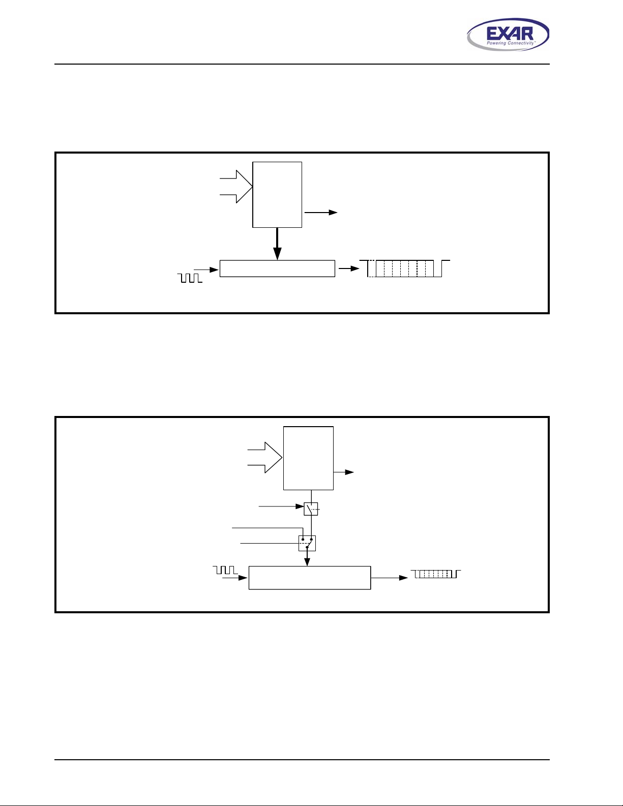
2.9.2 Transmitter Operation in non-FIFO Mode
The host loads transmit data to THR one character at a time. The THR empty flag (LSR bit-5) is set when the
data byte is transferred to TSR. THR fl ag can ge nerate a tr ansmit emp ty inter rupt (ISR bit -1) when it is enable d
by IER bit-1. The TSR flag (LSR bit-6) is set when TSR becomes completely empty.
F
IGURE
8. T
RANSMITTER OPERATION IN NON
Data
Byte
16X or 8X or 4X
Clock
( DLD[5:4] )
-FIFO M
Transmit Shift Register (TSR)
ODE
Transmit
Holding
Register
(THR)
THR Interrupt (ISR bit-1)
Enabled by IER bit-1
M
S
B
L
S
B
TXNOFIFO1
2.9.3 Transmitter Operation in FIFO Mode
The host may fill the transmit FIFO with up to 64 bytes of transmit data. The THR empty flag (LSR bit-5) is set
whenever the FIFO is empty. The THR empty flag can generate a transmit empty interrupt (ISR bit-1) when the
FIFO becomes empty. The transmit empty interrupt is enabled by IER bit-1. The TSR flag (LSR bit-6) is set
when TSR/FIFO becomes empty.
F
IGURE
9. T
RANSMITTER OPERATION IN
Auto CTS Flow Control (CTS# pin)
Flow Control Characters
(Xoff1/2 and Xon1/2 Reg.)
Auto Software Flow Co ntrol
16X or 8X or 4X Clock
(DLD[5 :4 ])
FIFO
Transmit
Data Byte
AND FLOW CONTROL MODE
Transmit
FIFO
Transmit Data Shift Register
(TSR)
THR Inte rr u p t (ISR b it-1 ) fa lls
below the programmed Trigger
Level and then when becomes
empty. FIFO is Enabled by FCR
bit-0=1
TXFIFO1
18
Page 19

XR16M654/654D
REV. 1.0.0
1.62V TO 3.63V QUAD UART WITH 64-BYTE FIFO
2.10 Receiver
The receiver section contains an 8-bit Receive Shift Register (RSR) and 64 bytes of FIFO which includes a
byte-wide Receive Holding Register (RHR). The RSR uses the 16X/8X/4X clock (DLD[5:4]) for timing. It
verifies and validates every bit on the incoming character in the middle of each data bit. On th e falling edge o f
a start or false start bit, an internal receiver counter starts counting a t the 16X/8X/4X clock rate . After 8 clocks
(or 4 if 8X or 2 if 4X) the start bit period should be at the center of the start bit. At this time the start bit is
sampled and if it is still a logic 0 it is validated. Evaluating the st ar t bit in t his manner p revent s t he receiver f rom
assembling a false character. The rest of the data bits and st op bits are sampled and validated in t his same
manner to prevent false framing. If t here we re any er ror( s), t hey are rep orted in th e LSR regist er bit s 2-4. Upon
unloading the receive data byte from RHR, the receive FIFO pointer is bumped and the error tags are
immediately updated to reflect the status of the data byte in RHR register. RHR can generate a receive data
ready interrupt upon receiving a character or delay until it reaches the FIFO trigger level. Furthermore, data
delivery to the host is guaranteed by a receive data ready time-out interrupt when data is not received for 4
word lengths as defined by LCR[1:0] plus 12 bits time. This is equivalent to 3.7-4.6 character times. The RHR
interrupt is enabled by IER bit-0. See
Figure 10 and Figure 11 below.
2.10.1 Receive Holding Register (RHR) - Read-Only
The Receive Holding Register is an 8-bit register that holds a receive data byte from the Receive Shift
Register. It provides the receive data interface to the host processor. The RHR register is part of the receive
FIFO of 64 bytes by 11-bits wide, the 3 extra bits are for the 3 error tags to be reported in LSR register. When
the FIFO is enabled by FCR bit-0, the RHR contains the first data character received by the FIFO. After the
RHR is read, the next character byte is loaded into the RHR and the errors associated with the current data
byte are immediately updated in the LSR bits 2-4.
F
IGURE
10. R
ECEIVER OPERATION IN NON
16X or 8X or 4X Clock
( DLD[5:4] )
Receive
Data By te
and Errors
-FIFO M
Receive Data Shift
Register (RSR)
Error
Tags in
LSR bits
4:2
ODE
Receive Data
Holding Register
(RHR)
Data Bit
Validation
Receive Data Characters
RHR Inte rrup t (IS R b it-2)
RXFIFO1
19
Page 20

XR16M654/654D
1.62V TO 3.63V QUAD UART WITH 64-BYTE FIFO
F
IGURE
11. R
ECEIVER OPERATION IN
16X or 8X or 4X Clock
( DLD[5:4] )
64 bytes by 11-bit wide
Receive Data
By te a n d E rrors
FIFO
FIFO
AND AUTO
Receive Data Shift
Register (RSR)
Receive
Da ta F IF O
(64-sets)
Error Tags
Receive
Data
LSR bits 4:2
Error Tags in
Da ta Bit
Va lida tion
Da ta fa l ls to
Trigger=16
Data fills to
RTS F
FIFO
56
LOW CONTROL MODE
Example
- RX FIFO trigger level selected at 16 bytes
:
8
(See Note Below)
RTS# re - a s s e rts wh e n data falls b elow th e flo w
con tr o l trig ger le v e l to r e s ta r t re mo te tr a nsmitter .
Enable by EFR bit-6=1, MCR bit-1.
RHR Interrupt (ISR bit-2) programmed for
desired FIFO trigger level.
FIFO is Enabled by FCR bit-0=1
RTS# de-asserts when data fills above the flow
control trigger level to suspend remo te transmitter.
Enable by EFR bit-6=1, MCR bit-1.
REV. 1.0.0
Receive Data Characters
RXFIFO1
2.11 Auto RTS (Hardware) Flow Control
Automatic RTS hardware flow control is used to prevent data overrun to the local receiver FIFO. The RTS#
output is used to request remote unit to suspend/resume data transmission. The auto RTS flow control
features is enabled to fit specific applicatio n req uir em e nt (see
•
Enable auto RTS flow control using EFR bit-6.
•
The auto RTS function must be started by assert ing RTS# outpu t pin (MCR bit-1 to logic 1 af ter it is enabled).
Figure 12):
If using the Auto RTS interrupt:
Enable RTS interrupt through IER bit-6 (after setting EFR bit-4). The UART issues an interrupt when the RTS#
pin makes a transition from low to high: ISR bit-5 will be set to logic 1.
2.12 Auto RTS Hysteresis
The M654 has a new feature that provides flow control trigger hysteresis while maintaining compatibility with
the XR16C850, ST16C650A and ST16C550 family of UARTs. With the Auto RTS function enabled, an interrupt
is generated when the receive FIFO reaches the selected RX trigger level. The RTS# pin will not be forced
HIGH (RTS off) until the receive FIFO reaches one trigger level above the selected trigger level in the trigger
table (
Table 12). The RTS# pin will return LOW after the RX FIFO is unloaded to one level below the selected
trigger level. Under the above described conditions, the M654 will continue to accept data until the receive
FIFO gets full. The Auto RTS function is initiated when the RTS# output pin is asserted LOW (RTS On).
T
ABLE
7: A
UTO
RX T
RIGGER LEVEL
INT PIN A
RTS (H
CTIVATION
ARDWARE
) F
RTS# DE-
(C
HARACTERS IN RX FIFO
LOW CONTROL
ASSERTED
(H
IGH
)
RTS# A
)
(C
SSERTED
HARACTERS IN RX FIFO
(LOW)
)
8 8 16 0
16 16 56 8
56 56 60 16
60 60 60 56
20
Page 21

XR16M654/654D
REV. 1.0.0
1.62V TO 3.63V QUAD UART WITH 64-BYTE FIFO
2.13 Auto CTS Flow Control
Automatic CTS flow control is used to prevent data overrun to the remot e receiver FIFO. The CTS# input is
monitored to suspend/restart the local transmitter. The auto CTS flow control feature is selected to fit specific
application requirement (see
•
Enable auto CTS flow control using EFR bit-7.
Figure 12):
If needed, the CTS interrupt can be enabled through IER bit-7 (after setting EFR bit-4). The UART issues an
interrupt when the CTS# pin is de-asserted (HIGH): ISR bit-5 will be set to 1, and UART will suspend
transmission as soon as the stop bit of the character in process is shifted out. Transmission is resumed after
the CTS# input is re-asserted (LOW), indicating more data may be sent.
F
IGURE
12. A
UTO
RTS
AND
CTS F
Local UART
UARTA
Receiver FIFO
Trigger Reached
Auto RTS
Trigger Level
Transmitter
Auto CTS
Monitor
RTSA#
CTSB#
TXB
Data Starts
RXA FIFO
Receive
INTA
(RXA FIFO
Interrupt)
The local UART (UARTA) starts data transfer by asserting RTSA# (1). RTSA# is normally connected to CTSB# (2) of
remote UART (UARTB). CTSB# allows its transmitter to send data (3). TXB data arrives and fills UARTA receive FIFO
(4). When RXA data fills up to its receive FIFO trigger level, UARTA activates its RXA data ready interrupt (5) and con
tinues to receive and put data into its FIFO. If interrupt service latency is long and data is not being unloaded, UARTA
monitors its receive data fill level to match the upper threshold of RTS delay and de-assert RTSA# (6). CTSB# follows
(7) and request UARTB transmitter to suspend data transfer. UARTB stops or finishes sending the data bits in its transmit shift register (8). When receive FIFO data in UARTA is unloaded to match the lower threshold of RTS delay (9),
UARTA re-asserts RTSA# (10), CTSB# recognizes the change (11) and restarts its transmitter and data flow again until
next receive FIFO trigger (12). This same event applies to the reverse direction when UARTA sends data to UARTB
with RTSB# and CTSA# controlling the data flow.
Data
LOW CONTROL OPERATION
RXA TXB
RTSA# CTSB#
Assert RTS# to Begin
Transmission
1
ON
2
ON
3
4
RX FIFO
Trigger Level
5
7
8
6
RTS High
Threshold
OFF
OFF
Suspend
RXBTXA
RTSB#CTSA#
Restart
9
RTS Low
Threshold
Remote UART
Trigger Reached
10
ON
11
UARTB
Transmitter
Auto CTS
Monitor
Receiver FIFO
Auto RTS
Trigger Level
ON
RX FIFO
12
Trigger Level
RTSCTS1
-
21
Page 22

XR16M654/654D
1.62V TO 3.63V QUAD UART WITH 64-BYTE FIFO
REV. 1.0.0
2.14 Auto Xon/Xoff (Software) Flow Control
When software flow control is enabled (See Table 16), the M654 compares one or two sequential receive data
characters with the programmed Xon or Xoff-1,2 character value(s). If receive character(s) (RX) match the
programmed values, the M654 will halt tran smission (TX) as soon as the current character has completed
transmission. When a match occurs, the Xoff (if enabled via IER bit-5) flag will be set and the interrupt output
pin will be activated. Following a suspension due to a match of the Xoff character, the M654 will monitor the
receive data stream for a match to the Xon-1,2 character. If a match is found, the M654 will resume operation
and clear the flags (ISR bit-4).
Reset initially sets the contents of the Xon/Xoff 8-bit flow control registers to a logic 0. Following reset the user
can write any Xon/Xoff value desired for software flow control. Different conditions can be set to detect Xon/
Xoff characters (
See Table 16) and suspend/resume transmissions. When double 8-bit Xon/Xoff characters
are selected, the M654 compares two consecutive receive characters with two software flow control 8-bit
values (Xon1, Xon2, Xoff1, Xoff2) and controls TX transmissions accordingly. Under the above described flow
control mechanisms, flow control characters are not placed (stacked) in the user accessible RX data buffer or
FIFO.
In the event that the receive buffer is overfilling and flow control needs to be executed, the M654 automatically
sends an Xoff message (when enabled) via the serial TX output to the remote modem. The M654 sends the
Xoff-1,2 characters two-character- times (= time taken to send two characte rs at the programmed baud rate )
after the receive FIFO crosses the programmed trigger level. To clear this condition, the M654 will transmit the
programmed Xon-1,2 characters as soon as receive FIFO is less t ha n on e trigg er level be low th e pr ogra mme d
trigger level.
Table 8 below explains this.
T
ABLE
8: A
UTO XON/XOFF
RX T
RIGGER LEVEL
8 8 8* 0
16 16 16* 8
56 56 56* 16
60 60 60* 56
* After the trigger level is reached, an xoff character is sent after a short span of time (= time required to send 2 characters);
for example, after 2.083ms has elapsed for 9600 baud and 10-bit word length setting.
INT PIN A
CTIVATION
(S
OFTWARE
X
OFF CHARACTER(S
CHARACTERS IN RX FIFO
(
) F
LOW CONTROL
) S
ENT
)
XON C
HARACTER(S
CHARACTERS IN RX FIFO
(
) S
ENT
)
2.15 Special Character Detect
A special character detect feature is provided to detect an 8-bit character when bit-5 is set in the Enhanced
Feature Register (EFR). When this character (Xoff2) is detected, it will be placed in the FIFO along with normal
incoming RX data.
The M654 compares each incoming receive character with Xoff-2 data. If a match exists, the received data will
be transferred to the RX FIFO and ISR bit-4 will be set to indicate detection of special character. Although the
Internal Register Table shows Xon, Xoff Registers with eight bits of character information, the actual number of
bits is dependent on the programmed word length. Line Control Register (LCR) bits 0-1 defines the number of
character bits, i.e., either 5 bits, 6 bits, 7 bits, or 8 bits. The word length selected by LCR bits 0-1 also
determines the number of bits that will be used for the special character comparison. Bit-0 in the Xon, Xoff
Registers corresponds with the LSB bit for the receive character.
22
Page 23

XR16M654/654D
REV. 1.0.0
1.62V TO 3.63V QUAD UART WITH 64-BYTE FIFO
2.16 Infrared Mode
The M654 UART includes the infrared encode r and de coder compatible to the IrDA (Infrared Dat a Associ ation)
version 1.0. The IrDA 1.0 standard that stipulates the infrared encoder sends out a
3/16 of a bit wide HIGHpulse for each “0” bit in the transmit dat a str eam. This signal encoding red uces the on-ti me of the infrar ed LED,
hence reduces the power consumption. See
Figure 13 below.
The infrared encoder and decoder are enable d by settin g MCR reg ist er bit -6 to a ‘1’. When t he infrar ed fe at ure
is enabled, the transmit data output, TX, idles at logic zero level. Likewise, the RX input assumes an idle level
of logic zero from a reset and power up, see
Figure 13.
Typically, the wireless infrared decoder receives the input pulse from the infrared sensing diode on the RX pin.
Each time it senses a light pulse, it returns a logic 1 to the data bit stream.
F
IGURE
13. I
NFRARED TRANSMIT DATA ENCODING AND RECEIVE DATA DECODING
Character
Data B its
3/16 Bit Time
TX Data
Transmit
IR Pulse
(TX Pin)
Start
11 111
0000 0
Bit Time
Stop
1/2 Bit Time
IrEnco der-1
Receive
IR Pulse
(RX pin)
RX Data
Bit Time
1/16 Clock Delay
11 111
0000 0
Start
Data Bits
Character
Stop
IRdecoder-1
23
Page 24

XR16M654/654D
1.62V TO 3.63V QUAD UART WITH 64-BYTE FIFO
REV. 1.0.0
2.17 Sleep Mode with Auto Wake-Up
The M654 supports low voltage system designs, hence, a sleep mode is included to reduce its power
consumption when the chip is not actively used.
All of these conditions must be satisfied for the M654 to enter sleep mode:
■
no interrupts pending for all four channels of the M654 (ISR bit-0 = 1)
■
sleep mode of all channels are enabled (IER bit-4 = 1)
■
modem inputs are not toggling (MSR bits 0-3 = 0)
■
RX input pins are idling HIGH
The M654 stops its crystal oscillator to conserve power in the sleep mode. User can check the XTAL2 pin for
no clock output as an indication that the device has entered the sleep mode.
The M654 resumes normal operation by any of the following:
■
a receive data start bit transition (HIGH to LOW)
■
a data byte is loaded to the transmitter, THR or FIFO
■
a change of logic state on any of the modem or general purpose serial inputs: CTS#, DSR#, CD#, RI#
If the M654 is awakened by any one of the above co nd itions, it will r et urn t o the sle ep mode au to mati cally after
all interrupting conditions have been se rviced and cleared. If the M654 is awakened by the modem inputs, a
read to the MSR is required to reset the modem inputs. In any case, the sleep mode will not be entered while
an interrupt is pending from a ny chan nel. The M654 w ill stay in the slee p mod e of op eration u ntil it is dis abled
by setting IER bit-4 to a logic 0.
If the address lines, data bus lines, IOW#, IOR#, CSA#, CSB#, CSC#, CSD# and modem input lines remain
steady when the M654 is in sleep mode, the maximum cur rent will b e in the micr oamp range as specified in the
DC Electrical Characteristics on
page 42. If the input lines are floating or are toggling while the M654 is in
sleep mode, the current can be up to 100 times more. If any of those signals are toggling or floating, then an
external buffer would be required to keep the address, data and control lines steady to achieve the low current.
A word of caution: owing to the starting up delay of the crystal oscillator after waking up from sleep mode, the
first few receive characters may be lost. Also, make sure the RX A-D pins are idling HIGH or “marking”
condition during sleep mode. This ma y n ot occur when the external interface transceivers (RS-232, RS-485 or
another type) are also put to sleep mode and cannot maintain the “marking” condition. To avoid this, the
system design engineer can use a 47k ohm pull-up resistor on each of the RX A-D inputs.
2.18 Internal Loopback
The M654 UART provides an internal loopback capability for system diagnostic purposes. The internal
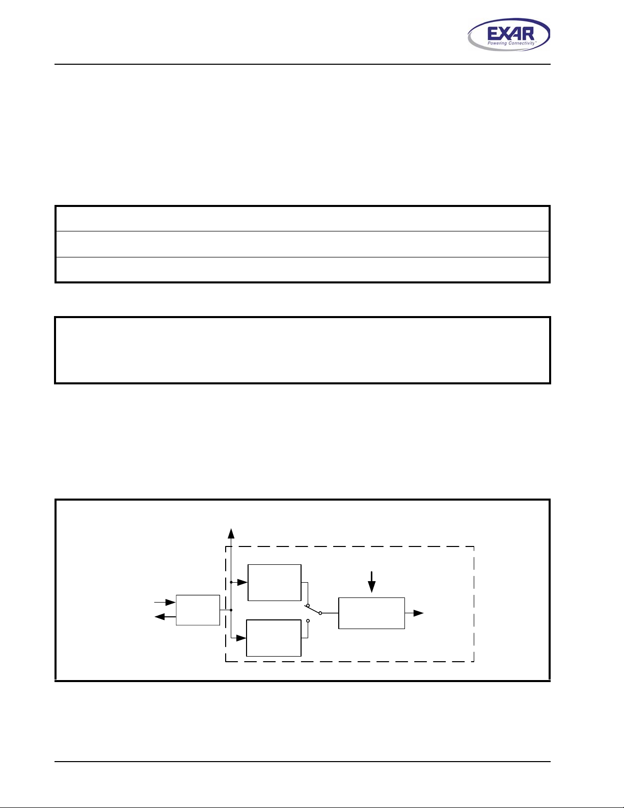
loopback mode
is enabled by setting MCR register bit-4 to logi c 1. All regular UAR T functions op erate normally.
Figure 14 shows how the modem port signals are re-configured. Transmit data from the transmit shift register
output is internally routed to the receive shift register input allowing the system to receive the same data that it
was sending. The TX pin is held HIGH or mark condition while RTS# and DTR# are de-asserted, and CTS#,
DSR# CD# and RI# inputs are ignored. Caution: the RX input must be held HIGH during loopback test else
upon exiting the loopback test the UART may detect and report a false “break” signal.
24
Page 25

XR16M654/654D
REV. 1.0.0
F
IGURE
14. I
NTERNAL LOOP BACK IN CHANNELS
Transmit Shift Register
Receive Shift Register
(THR/FIFO)
(RHR/FIFO)
A - D
MCR bit-4=1
RTS#
CTS#
1.62V TO 3.63V QUAD UART WITH 64-BYTE FIFO
VCC
TX A-D
RX A-D
VCC
RTS# A-D
CTS# A-D
VCC
Internal Data Bus Lines and Control Signals
Modem / General Purpose Control Logic
DTR#
DSR#
RI#
CD#
OP1#
OP2#
DTR# A-D
DSR# A-D
RI# A-D
CD# A-D
25
Page 26

XR16M654/654D
1.62V TO 3.63V QUAD UART WITH 64-BYTE FIFO
REV. 1.0.0
3.0 UART INTERNAL REGISTERS
Each UART channel in the M654 has its own set of configuration registers selected by address lines A0, A1
and A2 with a specific channel selected (See
Table 1 and Table 2). The complete register set is shown on
Table 9 and Table 10.
.
T
ABLE
9: UART CHANNEL A AND B UART INTERNAL REGISTERS
A2,A1,A0 A
DDRESSES
0 0 0 RHR - Receive Holding Register
R
EGISTER
16C550 C
THR - Transmit Holding Register
OMPATIBLE REGISTERS
R
EAD/WRITE
Read-only
Write-only
0 0 0 DLL - Divisor LSB Read/Write
0 1 0 DLD - Divisor Fractional Read/Write
0 0 1 IER - Interrupt Enable Register Read/Write
0 1 0 ISR - Interrupt Status Register
FCR - FIFO Control Register
Read-only
Write-only
LCR[7] = 1, LCR ≠ 0xBF0 0 1 DLM - Divisor MSB Read/Write
C
OMMENTS
LCR[7] = 0
LCR[7] = 0
0 1 1 LCR - Line Control Register Read/Write
1 0 0 MCR - Modem Control Register Read/Write
1 0 1 LSR - Line Status Register Read-only
LCR[7] = 0
1 1 0 MSR - Modem Status Register Read-only
1 1 1 SPR - Scratch Pad Register Read/Write
E
NHANCED REGISTERS
0 1 0 EFR - Enhanced Function Reg Read/Write
1 0 0 Xon-1 - Xon Character 1 Read/Write
1 0 1 Xon-2 - Xon Character 2 Read/Write
LCR = 0xBF
1 1 0 Xoff-1 - Xoff Character 1 Read/Write
1 1 1 Xoff-2 - Xoff Character 2 Read/Write
X X X FSTAT - FIFO Status Register Read-only FSRS# pin is LOW
26
Page 27

XR16M654/654D
REV. 1.0.0
A
DDRESS
A2-A0
T
ABLE
10: INTERNAL REGISTERS DESCRIPTION.
R
EG
R
EAD
/
N
AME
W
RITE
BIT-7 BIT-6 BIT-5 BIT-4 BIT-3 BIT-2 BIT-1 BIT-0 C
1.62V TO 3.63V QUAD UART WITH 64-BYTE FIFO
S
HADED BITS ARE ENABLED WHEN
16C550 Compatible Registers
0 0 0 RHR RD Bit-7 Bit-6 Bit-5 Bit-4 Bit-3 Bit-2 Bit-1 Bit-0
0 0 0 THR WR Bit-7 Bit-6 Bit-5 Bit-4 Bit-3 Bit-2 Bit-1 Bit-0
0 0 1 IER RD/WR 0/ 0/ 0/ 0/ Modem
CTS#
Int.
Enable
0 1 0 ISR RD FIFOs
Enabled
0 1 0 FCR WR R X F I F O
Trigger
RTS#
Int.
Enable
FIFOs
Enabled
R X FI F O
Trigger
Xoff Int.
Enable
Sleep
Mode
Enable
0/ 0/ INT
INT
Source
Bit-5
INT
Source
Bit-4
0/ 0/ DMA
TX FIFO
Trigger
TX FIF O
Trigger
Stat. Int.
Enable
Source
Bit-3
Mode
Enable
RX Line
Stat.
Int.
Enable
INT
Source
Bit-2
TX
FIFO
Reset
TX
Empty
Int
Enable
INT
Source
Bit-1
RX
FIFO
Reset
EFR BIT-4=1
RX
Data
Int.
Enable
INT
LCR[7] = 0
Source
Bit-0
FIFOs
Enable
OMMENT
0 1 1 LCR RD/WR Divisor
Enable
1 0 0 MCR RD/WR 0/ 0/ 0/ Internal
BRG
Pres-
caler
1 0 1 LSR RD RX FIFO
Global
Error
Set TX
Break
IR Mode
ENable
THR &
TSR
Empty
Set
Parity
XonAny
THR
Empty
Even
Parity
Parity
Enable
INT Out-
Lopback
Enable
put
Enable
(OP2#)
RX Break RX Fram-
ing Error
Stop
Bits
Rsvd
(OP1#)
RX
Parity
Error
Word
Length
Bit-1
RTS#
Output
Control
RX
Over-
run
Word
Length
Bit-0
DTR#
Output
Control
RX
Data
Ready
LCR[7] = 0
Error
1 1 0 MSR RD CD#
Input
RI#
Input
DSR#
Input
CTS#
Input
Delta
CD#
Delta
RI#
Delta
DSR#
Delta
CTS#
1 1 1 SPR RD/WR Bit-7 Bit-6 Bit-5 Bit-4 Bit-3 Bit-2 Bit-1 Bit-0
Baud Rate Generator Divisor
0 0 0 DLL RD/WR Bit-7 Bit-6 Bit-5 Bit-4 Bit-3 Bit-2 Bit-1 Bit-0 LCR[7]=1
0 0 1 DLM RD/WR Bit-7 Bit-6 Bit-5 Bit-4 Bit-3 Bit-2 Bit-1 Bit-0
LCR≠0xBF
0 1 0 DLD RD/WR Rsvd Rsvd 4X Mode 8X Mode Bit-3 Bit-2 Bit-1 Bit-0 LCR[7] = 1
LCR≠0xBF
EFR[4] = 1
27
Page 28

XR16M654/654D
1.62V TO 3.63V QUAD UART WITH 64-BYTE FIFO
T
ABLE
10: INTERNAL REGISTERS DESCRIPTION.
A
DDRESS
A2-A0
0 1 0 EFR RD/WR Auto
1 0 0 XON1 RD/WR Bit-7 Bit-6 Bit-5 Bit-4 Bit-3 Bit-2 Bit-1 Bit-0
1 0 1 XON2 RD/WR Bit-7 Bit-6 Bit-5 Bit-4 Bit-3 Bit-2 Bit-1 Bit-0
1 1 0 XOFF1 RD/WR Bit-7 Bit-6 Bit-5 Bit-4 Bit-3 Bit-2 Bit-1 Bit-0
1 1 1 XOFF2 RD/WR Bit-7 Bit-6 Bit-5 Bit-4 Bit-3 Bit-2 Bit-1 Bit-0
X X X FSTAT RD RX-
N
R
EG
AME
R
W
EAD
RITE
/
BIT-7 BIT-6 BIT-5 BIT-4 BIT-3 BIT-2 BIT-1 BIT-0 C
Enhanced Registers
CTS#
Enable
RDYD#
Auto
RTS#
Enable
RX-
RDYC#
Special
Char
Select
RX-
RDYB#
S
Enable
IER [7:4],
ISR [5:4],
FCR[5:4],
MCR[7:5],
DLD
RX-
RDYA#
HADED BITS ARE ENABLED WHEN
Software
Flow
Cntl
Bit-3
TX-
RDYD#
Software
Flow
Cntl
Bit-2
TX-
RDYC#
Software
Flow
Cntl
Bit-1
TX-
RDYB#
REV. 1.0.0
EFR BIT-4=1
Software
Flow
Cntl
Bit-0
LCR=0XBF
FSRS# pin is
TX-
RDYA#
a logic 0. No
address lines
required.
OMMENT
4.0 INTERNAL REGISTER DESCRIPTIONS
4.1 Receive Holding Register (RHR) - Read- Only
SEE”RECEIVER” ON PAGE 19.
4.2 Transmit Holding Register (THR) - Write-Only
SEE”TRANSMITTER” ON PAGE 17.
4.3 Interrupt Enable Register (IER) - Read/Write
The Interrupt Enable Register (IER) masks the interrupts from receive data ready, transmit empty, line status
and modem status registers. These interrupts are reported in the Interrupt Status Register (ISR).
4.3.1 IER versus Receive FIFO Interrupt Mode Operation
When the receive FIFO (FCR BIT-0 = 1) and receive interrupts (IER BIT-0 = 1) are enabled, the RHR inter rupt s
(see ISR bits 2 and 3) status will reflect the following:
A. The receive data available interrupts are issued to the host when the FIFO has reached the programmed
trigger level. It will be cleared when the FIFO drops below the programmed trigger level.
B. FIFO level will be reflected in the ISR register when the FIFO trigger level is reached. Both the ISR register
status bit and the interrupt will be cleared when the FIFO drops below the trigger level.
C. The r eceive d ata ready bit (LSR BIT-0) is set as soon as a character is transferr ed f rom th e shift register to
the receive FIFO. It is reset when the FIFO is empty.
28
Page 29

XR16M654/654D
REV. 1.0.0
4.3.2 IER versus Receive/Transmit FIFO Polled Mode Operation
When FCR BIT-0 equals a logic 1 for FIFO enable; resetting IER bits 0-3 enables the XR16M654 in the FIFO
polled mode of operation. Since the receiver and transmitter have separate bits in the LSR either or both can
be used in the polled mode by selecting respective transmit or receive control bit(s).
A. LSR BIT-0 indicates there is data in RHR or RX FIFO.
B. LSR BIT-1 indicates an overrun error has occurred and that data in the FIFO may not be valid.
C. LSR BIT 2-4 provides the type of receive data errors encountered for the data byte in RHR, if any.
D. LSR BIT-5 indicates THR is empty.
E. LSR BIT-6 indicates when both the transmit FIFO and TSR are empty.
F. LSR BIT-7 indicates a data error in at least one character in the RX FIFO.
IER[0]: RHR Interrupt Enable
The receive data ready interrupt will be issued when RHR has a dat a cha ra cter in the no n- FIF O mode or when
the receive FIFO has reached the programmed trigger level in the FIFO mode.
Logic 0 = Disable the receive data ready interrupt (default).
Logic 1 = Enable the receiver data ready interrupt.
IER[1]: THR Interrupt Enable
This bit enables the Transmit Ready interrupt which is issued whenever the THR becomes empty in the nonFIFO mode or when data in the FIFO falls below the programmed trigger level in the FIFO mode. If the THR is
empty when this bit is enabled, an interrupt will be generated.
1.62V TO 3.63V QUAD UART WITH 64-BYTE FIFO
Logic 0 = Disable Transmit Ready interrupt (default).
Logic 1 = Enable Transmit Ready interrupt.
IER[2]: Receive Line Status Interrupt Enable
If any of the LSR register bits 1, 2, 3 or 4 is a logic 1, it will generate an interrupt to inform the host controller
about the error status of the current data byte in FIFO. LSR bit-1 generates an interrupt immediately when an
overrun occurs. LSR bits 2-4 generate an interrupt when the character in the RHR has an error.
•
Logic 0 = Disable the receiver line status interrupt (default).
•
Logic 1 = Enable the receiver line status interrupt.
IER[3]: Modem Status Interrupt Enable
•
Logic 0 = Disable the modem status register interrupt (default).
•
Logic 1 = Enable the modem status register interrupt.
IER[4]: Sleep Mode Enable (requires EFR[4] = 1)
•
Logic 0 = Disable Sleep Mode (default).
•
Logic 1 = Enable Sleep Mode. See Sleep Mode section for further details.
IER[5]: Xoff Interrupt Enable (requires EFR[4]=1)
•
Logic 0 = Disable the software flow control, receive Xoff interrupt. (default)
•
Logic 1 = Enable the software flow control, receive Xoff interrupt. See Software Flow Control section for
details.
29
Page 30

XR16M654/654D
1.62V TO 3.63V QUAD UART WITH 64-BYTE FIFO
IER[6]: RTS# Output Interrupt Enable (requires EFR[4]=1)
•
Logic 0 = Disable the RTS# interrupt (default).
•
Logic 1 = Enable the RTS# interrupt. The UART issues an interrupt when the RTS# pin makes a transition
from LOW to HIGH (if enabled by EFR bit-6).
IER[7]: CTS# Input Interrupt Enable (requires EFR[4]=1)
•
Logic 0 = Disable the CTS# interrupt (default).
•
Logic 1 = Enable the CTS# interrupt. The UART issues an interrupt when CTS# pin makes a transition from
LOW to HIGH (if enabled by EFR bit-7).
4.4 Interrupt Status Register (ISR) - Read-Only
The UART provides multiple levels of prioritized interrupts to minimize external software interaction. The
Interrupt Status Register (ISR) provides the user with six interrupt status bits. Performing a read cycle on the
ISR will give the user the current highest pending interrupt level to be serviced, others are queued up to be
serviced next. No other interrupts are acknowledged until the pending interrupt is serviced. The Interrupt
Source Table,
associated with each of these interrupt levels.
4.4.1 Interrupt Generation:
•
LSR is by any of the LSR bits 1, 2, 3 and 4.
•
RXRDY is by RX trigger level.
Table 11, shows the data values (bit 0-5) for the interrupt priority levels and the interrupt sources
REV. 1.0.0
•
RXRDY Time-out is by a 4-char plus 12 bits delay timer.
•
TXRDY is by TX trigger level or TX FIFO empty.
•
MSR is by any of the MSR bits 0, 1, 2 and 3.
•
Receive Xoff/Special character is by detection of a Xoff or Special character.
•
CTS# is when the remote transmitter toggles t he input pin (from LOW to HIGH) during au to CTS flow control.
•
RTS# is when its receiver toggles the output pin (from LOW to HIGH) during auto RTS flow control.
4.4.2 Interrupt Clearing:
•
LSR interrupt is cleared by a read to the LSR register.
•
RXRDY interrupt is cleared by reading data until FIFO falls below the t rigger level.
•
RXRDY Time-out interrupt is cleared by reading RHR.
•
TXRDY interrupt is cleared by a read to the ISR register or writing to THR.
•
MSR interrupt is cleared by a read to the MSR register.
•
Xoff interrupt is cleared by a read to the ISR register or when XON character(s) is received.
•
Special character interrupt is cleared by a read to ISR register or after next character is received.
•
RTS# and CTS# flow control interrupts are cleared by a read to the MSR register.
30
Page 31

XR16M654/654D
REV. 1.0.0
]
T
ABLE
11: I
NTERRUPT SOURCE AND PRIORITY LEVEL
P
RIORITY
L
EVEL
1 0 0 0 1 1 0 LSR (Receiver Line Status Register)
2 0 0 1 1 0 0 RXRDY (Receive Data Time-out)
3 0 0 0 1 0 0 RXRDY (Received Data Ready)
4 0 0 0 0 1 0 TXRDY (Transmit Ready)
5 0 0 0 0 0 0 MSR (Modem Status Register)
6 0 1 0 0 0 0 RXRDY (Received Xoff or Special character)
7 1 0 0 0 0 0 CTS#, RTS# change of state
- 0 0 0 0 0 1 None (default)
BIT-5 BIT-4 BIT-3 BIT-2 BIT-1 BIT-0
ISR R
EGISTER STATUS BITS
1.62V TO 3.63V QUAD UART WITH 64-BYTE FIFO
S
OURCE OF INTERRUPT
ISR[0]: Interrupt Status
•
Logic 0 = An interrupt is pending and the ISR contents may be used as a pointer to the appropriate interrupt
service routine.
•
Logic 1 = No interrupt pending (default condition).
ISR[3:1]: Interrupt Status
These bits indicate the source for a pending interrupt at interrupt priority levels (See Interrupt Source
Table 11).
ISR[4]: Interrupt Status (requires EFR bit-4 = 1)
This bit is enabled when EFR bit-4 is set to a logic 1. IS R bit-4 indicates t hat the receiver det ected a dat a match
of the Xoff character(s) or a special character.
ISR[5]: Interrupt Status (requires EFR bit-4 = 1)
ISR bit-5 indicates that CTS# or RTS# has changed state from LOW to HIGH.
ISR[7:6]: FIFO Enable Status
These bits are set to a logic 0 when the FIFOs are disabled. They are set to a logic 1 when the FIFOs are
enabled.
4.5 FIFO Control Register (FCR) - Write-Only
This register is used to enable the FIFOs, clear the FIFOs, set the transmit/receive FIFO trigger levels, and
select the DMA mode. The DMA, and FIFO modes are defined as follows:
FCR[0]: TX and RX FIFO Enable
•
Logic 0 = Disable the transmit and receive FIFO (default).
•
Logic 1 = Enable the transmit and receive FIFOs. This bit must be set to logic 1 when other FCR bits are
written or they will not be programmed.
31
Page 32

XR16M654/654D
1.62V TO 3.63V QUAD UART WITH 64-BYTE FIFO
REV. 1.0.0
FCR[1]: RX FIFO Reset
This bit is only active when FCR bit-0 is a ‘1’.
•
Logic 0 = No receive FIFO reset (default)
•
Logic 1 = Reset the receive FIFO pointers and FIFO level counter logic (the receive shift register is not
cleared or altered). This bit will return to a logic 0 after resetting the FIFO.
FCR[2]: TX FIFO Reset
This bit is only active when FCR bit-0 is a ‘1’.
•
Logic 0 = No transmit FIFO reset (default).
•
Logic 1 = Reset the transmit FIFO pointers and FIFO level counter logic (the transmit shift register is not
cleared or altered). This bit will return to a logic 0 after resetting the FIFO.
FCR[3]: DMA Mode Select
Controls the behavior of the -TXRDY and -RXRDY pins. See DMA operation section for details.
•
Logic 0 = Normal Operation (default).
•
Logic 1 = DMA Mode.
FCR[5:4]: Transmit FIFO Trigger Select (requires EFR bit-4 = 1)
(logic 0 = default, TX trigger level = one)
These 2 bits set the trigger level for the transmit FIFO. The UART will issue a transmit interrupt when the
number of characters in the FIFO falls below the selected trigger level, or when it gets empty in case that the
FIFO did not get filled over the trigger level on last re-load.
Table 12 below shows the selections.
FCR[7:6]: Receive FIFO Trigger Select
(logic 0 = default, RX trigger level =1)
These 2 bits are used to set the trigger level for the receive FIFO. The UART will issue a receive interrupt when
the number of the characters in the FIFO c rosse s the trig ge r lev el.
T
ABLE
12: T
FCR
BIT-7
0
0
1
1
RANSMIT AND RECEIVE
FCR
BIT-6
FCR
BIT-5
0
0
1
1
0
1
0
1
FCR
BIT
-4
0
1
0
1
FIFO T
R
T
Table 12 shows the complete selections.
RIGGER LEVEL SELECTION
ECEIVE
T
RIGGER
EVEL
L
8
16
56
60
RANSMIT
RIGGER
T
L
EVEL
8
16
32
56
32
Page 33

XR16M654/654D
REV. 1.0.0
1.62V TO 3.63V QUAD UART WITH 64-BYTE FIFO
4.6 Line Control Register (LCR) - Read/Write
The Line Control Register is used to specify the asynchronous data communication format. The word or
character length, the number of stop bits, and the parity are selected by writing the appropriate bits in this
register.
LCR[1:0]: TX and RX Word Length Select
These two bits specify the word length to be transmitted or received.
BIT-1 BIT-0 W
0 0 5 (default)
0 1 6
1 0 7
1 1 8
ORD LENGTH
LCR[2]: TX and RX Stop-bit Length Select
The length of stop bit is specified by this bit in conjunction with the programmed word length.
S
W
ORD
BIT-2
0 5,6,7,8 1 (default)
1 5 1-1/2
1 6,7,8 2
LENGTH
TOP BIT LENGTH
(BIT
TIME(S
))
LCR[3]: TX and RX Parity Select
Parity or no parity can be selected via this bit. The parity bit is a simple way used in communications for data
integrity check. See
•
Logic 0 = No parity.
•
Logic 1 = A parity bit is generated during the transmission while the receiver checks for parity error of the
Table 13 for parity selection summary below.
data character received.
LCR[4]: TX and RX Parity Select
If the parity bit is enabled with LCR bit-3 set to a logic 1, LCR BIT-4 selects the even or odd parity format.
•
Logic 0 = ODD Parity is generated by forcing an odd number of logic 1’s in the transmitted character. The
receiver must be programmed to check the same format (default).
•
Logic 1 = EVEN Parity is generated by forcing an even number of logic 1’s in the transmitted character. The
receiver must be programmed to check the same format.
33
Page 34

XR16M654/654D
1.62V TO 3.63V QUAD UART WITH 64-BYTE FIFO
LCR[5]: TX and RX Parity Select
If the parity bit is enabled, LCR BIT-5 selects the forced parity format.
•
LCR BIT-5 = logic 0, parity is not forced (default).
•
LCR BIT-5 = logic 1 and LCR BIT-4 = logic 0, parity bit is forced to a logical 1 for the transmit and receive
data.
•
LCR BIT-5 = logic 1 and LCR BIT-4 = logic 1, parity bit is forced to a logical 0 for the transmit and receive
data.
T
ABLE
13: P
ARITY SELECTION
LCR BIT-5 LCR BIT-4 LCR BIT-3 P
X X 0 No parity
0 0 1 Odd parity
0 1 1 Even parity
1 0 1 Force parity to mark, HIGH
1 1 1 Forced parity to space, LOW
LCR[6]: Transmit Break Enable
ARITY SELECTION
REV. 1.0.0
When enabled, the Break control bit causes a break condition to be transmitted (the TX output is forced to a
“space’, logic 0, state). This condition remains, until disabled by setting LCR bit-6 to a logic 0.
•
Logic 0 = No TX break condition. (default)
•
Logic 1 = Forces the transmitter output (TX) to a “space”, logic 0, for alerting the remote receiver of a line
break condition.
LCR[7]: Baud Rate Divisors Enable
Baud rate generator divisor (DLL/DLM/DLD) enable.
•
Logic 0 = Data registers are selected. (default)
•
Logic 1 = Divisor latch registers are selected.
4.7 Modem Control Register (MCR) or General Purpose Outputs Control - Read/Write
The MCR register is used for controlling the serial/modem interface signals or general purpose inputs/outputs.
MCR[0]: DTR# Output
The DTR# pin is a modem control output. If the modem interface is not used, this output may be used as a
general purpose output.
•
Logic 0 = Force DTR# output HIGH (default).
•
Logic 1 = Force DTR# output LOW.
MCR[1]: RTS# Output
The RTS# pin is a modem control output and may be used for automatic hardware flow control by enabled by
EFR bit-6. If the modem interface is not used, this output may be used as a general purpose output.
•
Logic 0 = Force RTS# output HIGH (default).
•
Logic 1 = Force RTS# output LOW.
34
Page 35

XR16M654/654D
REV. 1.0.0
MCR[2]: Reserved
OP1# is not available as an output pin on the M654. But it is available for use during Internal Loopback Mode.
In the Loopback Mode, this bit is used to write the state of the modem RI# interface signal.
MCR[3]: INT Output Enable
Enable or disable INT outputs to becom e active or in th ree-state. Th is func tion is as sociat ed with t he INTSE L
input, see below table for details. This bit is also used to control the OP2# signal during internal loopback
mode.
•
•
INTSEL pin must be LOW during 68 mode.
Logic 0 = INT (A-D) outputs disabled (three state) in the 16 mode (default). During internal loopback mode,
OP2# is HIGH.
Logic 1 = INT (A-D) outputs enabled (active) in the 16 mode. During internal loopback mode, OP2# is LOW.
T
ABLE
14: INT O
INTSEL
P
MCR
IN
BIT-3
0 0 Three-State
0 1 Active
1 X Active
1.62V TO 3.63V QUAD UART WITH 64-BYTE FIFO
UTPUT MODES
INT A-D O
UTPUTS IN
16 M
ODE
MCR[4]: Internal Loopback Enable
•
Logic 0 = Disable loopback mode (default).
•
Logic 1 = Enable local loopback mode, see loopback section and Figure 14.
MCR[5]: Xon-Any Enable (requires EFR bit-4 = 1)
•
Logic 0 = Disable Xon-Any function (for 16C550 compatibility, default).
•
Logic 1 = Enable Xon-Any function. In this mode, any RX character received will resume transmit operation.
The RX character will be loaded into the RX FIFO , unless the RX character is an Xon or Xoff character and
the M654 is programmed to use the Xon/Xoff flow control.
MCR[6]: Infrared Encoder/Decoder Enable (requires EFR bit-4 = 1)
•
Logic 0 = Enable the standard modem receive and transmit input/output interface. (Default)
•
Logic 1 = Enable infrared IrDA receive and transmit inputs/outputs. The TX/RX ou tp ut /i npu t ar e ro ut ed to the
infrared encoder/decoder. The data input and output levels conform to the IrDA infrared interface
requirement. The RX FIFO may need to be flushed upon enable. While in this mode, the infrared TX output
will be LOW during idle data conditions.
MCR[7]: Clock Prescaler Select (requires EFR bit-4 = 1)
•
Logic 0 = Divide by one. The input clock from the crysta l or external clock is fed directly to the Pr ogrammabl e
Baud Rate Generator without further modification, i.e., divide by one (default).
•
Logic 1 = Divide by four. The prescaler divides the input clock from the crystal or external clock by four and
feeds it to the Programmable Baud Rate Generator, hence, data rates become one forth.
35
Page 36

XR16M654/654D
1.62V TO 3.63V QUAD UART WITH 64-BYTE FIFO
4.8 Line Status Register (LSR) - Read Only
This register provides the status of data transfers between the UART and the host. If IER bit-2 is enabled, LSR
bit 1 will generate an interrupt immediately and LSR bits 2-4 will generate an interrupt when a character with an
error is in the RHR.
LSR[0]: Receive Data Ready Indicator
•
Logic 0 = No data in receive holding register or FIFO (default).
•
Logic 1 = Data has been received and is saved in the receive holding register or FIFO.
LSR[1]: Receiver Overrun Flag
•
Logic 0 = No overrun error (default).
•
Logic 1 = Overrun error. A data overrun error condition occurred in the receive shift register. This happens
when additional data arrives while the FIFO is full. In this case the previous data in the receive shift register
is overwritten. Note that under this condition the data byte in the receive shift register is not transferred into
the FIFO, therefore the data in the FIFO is not corr up te d by the error.
LSR[2]: Receive Data Parity Error Tag
•
Logic 0 = No parity error (default).
•
Logic 1 = Parity error. The receive character in RHR does not have correct parity information and is suspect.
This error is associated with the character available for reading in RHR.
REV. 1.0.0
LSR[3]: Receive Data Framing Error Tag
•
Logic 0 = No framing error (default).
•
Logic 1 = Framing error. The receive character did not have a valid stop bit(s). This error is associated with
the character available for reading in RHR.
LSR[4]: Receive Break Tag
•
Logic 0 = No break condition (default).
•
Logic 1 = The receiver received a break signal (RX was LOW for at least one character fr ame time). In the
FIFO mode, only one break character is loaded into the FIFO. The break indication remains until the RX
input returns to the idle condition, “mark” or HIGH.
LSR[5]: Transmit Holding Register Empty Flag
This bit is the Transmit Holding Re gister Empty indi cator. The THR bit is set to a logic 1 when the last data byte
is transferred from the transmit holding register to the transmit shift register. The bit is reset to logic 0
concurrently with the data loading to the transmit holding register by the host. In the FIFO mode this bit is set
when the transmit FIFO is empty, it is cleared when the transmit FIFO contains at least 1 byte.
LSR[6]: THR and TSR Empty Flag
This bit is set to a logic 1 whenever the transmitter goes idle. It is set to logic 0 whenever either the THR or
TSR contains a data character. In the FIFO mode this bit is set to a logic 1 whenever the transmit FIFO and
transmit shift register are both empty.
LSR[7]: Receive FIFO Data Error Flag
•
Logic 0 = No FIFO error (default).
•
Logic 1 = A global indicator for the sum of all error bit s in t he RX FIFO. At least one p ar ity err or, framing error
or break indication is in the FIFO data. This bit clears when there is no more error(s) in any of the bytes in the
RX FIFO.
36
Page 37

XR16M654/654D
REV. 1.0.0
4.9 Mode m Status Regist er (MSR) - Rea d On ly
This register provides the current state of the modem interface input signals. Lower four bits of this register are
used to indicate the changed information. These bits are set to a logic 1 whenever a signal from the modem
changes state. These bits may be used for general purpose inputs when they are not used with modem
signals.
MSR[0]: Delta CTS# Input Flag
•
Logic 0 = No change on CTS# input (default).
•
Logic 1 = The CTS# input has changed state since the last time it was monitored. A modem status interrupt
will be generated if MSR interrupt is enabled (IER bit-3).
MSR[1]: Delta DSR# Input Flag
•
Logic 0 = No change on DSR# input (default).
•
Logic 1 = The DSR# input has changed state since the last time it was mo nitored. A mo dem status inte rrupt
will be generated if MSR interrupt is enabled (IER bit-3).
MSR[2]: Delta RI# Input Flag
•
Logic 0 = No change on RI# input (default).
•
Logic 1 = The RI# input has changed from LOW to HIGH, ending of the ringing signal. A modem status
interrupt will be generated if MSR interrupt is enabled (IER bit-3).
1.62V TO 3.63V QUAD UART WITH 64-BYTE FIFO
MSR[3]: Delta CD# Input Flag
•
Logic 0 = No change on CD# input (default).
•
Logic 1 = Indicates that the CD# input has changed state since the last time it was monitored. A modem
status interrupt will be generated if MSR interrupt is enabled (IER bit-3).
MSR[4]: CTS Input Status
CTS# pin may function as automatic hardware flow control signal input if it is enabled and selected by Auto
CTS (EFR bit-7). Auto CTS flow control allows starting and stopping of local data transmissions based on the
modem CTS# signal. A HIGH on the CTS# pin will stop UAR T tr ansmit ter as soon as the cur rent ch aracter h as
finished transmission, and a LOW will resum e data transmission. Normally MSR bit-4 bit is the compliment of
the CTS# input. However in the loopback mode, this bit is equivalent to the RTS# bit in the MCR register. The
CTS# input may be used as a general purpose input when the modem interface is not used.
MSR[5]: DSR Input Status
Normally this bit is the complement of the DSR# input. In the loopback mode, this bit is equiva len t to th e DTR#
bit in the MCR register. The DSR# input may be used as a general purpose input when the modem interface is
not used.
MSR[6]: RI Input Status
Normally this bit is the complement of the RI# input. In the loopback mode this bit is equivalent to bit-2 in th e
MCR register. The RI# input may be used as a general purpose input when the modem interfa ce is not us ed .
MSR[7]: CD Input Status
Normally this bit is the complement of the CD# inpu t. In the loopba ck mode th is bit is equivalen t to bit-3 in the
MCR register. The CD# input may be used as a general purpose input when the modem interfa ce is not us ed .
4.10 Scratch Pad Register (SPR) - Read/Write
This is a 8-bit general purpose register for the user to store temporary data. The content of this register is
preserved during sleep mode but becomes 0xFF (default) after a reset or a power off-on cycle.
37
Page 38

XR16M654/654D
1.62V TO 3.63V QUAD UART WITH 64-BYTE FIFO
REV. 1.0.0
4.11 Baud Rate Generator Registers (DLL and DLM) - Read/Write
These registers make-up the value of the baud ra te divisor. The concatenation of the contents of DLM and DLL
gives the 16-bit divisor value. Then the value is added to DLD[3:0]/16 to achieve the fractional baud rate
divisor. DLD must be enabled via EFR bit-4 before it can be accessed. See
Table 15 below and See ”Section
2.8, Programmable Baud Rate Generator with Fractional Divisor” on page 15.
DLD[5:4]: Sampling Rate Select
These bits select the dat a sa mpli ng rat e. By def ault, t he d at a samp ling rat e is 16X. The ma ximum dat a rat e will
double if the 8X mode is selected and will quadruple if the 4X mode is selected. See
T
ABLE
15: S
AMPLING RATE SELECT
DLD[5] DLD[4] S
0 0 16X
0 1 8X
1 X 4X
Table 15 below.
AMPLING RATE
DLD[7:6]: Reserved
4.12 Enhanced Feature Register (EFR) - Read/Write
Enhanced features are enabled or disabled using this register. Bit 0-3 provide single or dual consecutive
character software flow control selection (see
Table 16). When the Xon1 and Xon2 and Xoff1 and Xoff2 modes
are selected, the double 8-bit words are concatenated into two sequential characters. Caution: note that
whenever changing the TX or RX flow control bits, always reset all bits back to logic 0 (disable) before
programming a new setting.
EFR[3:0]: Software Flow Control Select
Single character and dual sequential characters software flow control is supported. Combinations of software
flow control can be selected by programming these bits.
38
Page 39

XR16M654/654D
REV. 1.0.0
EFR
C
ONT
1.62V TO 3.63V QUAD UART WITH 64-BYTE FIFO
T
ABLE
16: S
OFTWARE FLOW CONTROL FUNCTIONS
BIT
-3
-3
0 0 0 0 No TX and RX flow control (default and reset)
0 0 X X No transmit flow control
1 0 X X Transmit Xon1, Xoff1
0 1 X X Transmit Xon2, Xoff2
1 1 X X Transmit Xon1 and Xon2, Xoff1 and Xoff2
X X 0 0 No receive flow con trol
X X 1 0 Receiver compares Xon1, Xoff1
X X 0 1 Receiver compares Xon2, Xoff2
1 0 1 1 Transmit Xon1, Xoff1
0 1 1 1 Transmit Xon2, Xoff2
EFR
C
ONT
BIT
-2
-2
EFR
C
ONT
BIT
-1
-1
EFR
C
ONT
BIT
-0
T
-0
RANSMIT AND RECEIVE SOFTWARE FLOW CONTROL
Receiver compares Xon1 or Xon2, Xoff1 or Xoff2
Receiver compares Xon1 or Xon2, Xoff1 or Xoff2
1 1 1 1 Transmit Xon1 and Xon2, Xoff1 and Xoff2,
Receiver compares Xon1 and Xon2, Xoff1 and Xoff2
0 0 1 1 No transmit flow control,
Receiver compares Xon1 and Xon2, Xoff1 and Xoff2
EFR[4]: Enhanced Function Bits Enable
Enhanced function control bit. This bit enables IER bits 4-7, ISR bits 4-5, FCR bits 4-5, MCR bits 5-7, and DLD
to be modified. After modifying any enhanced bits, EFR bit-4 can be set to a logic 0 to latch the new values.
This feature prevents legacy sof twar e fr om alter ing or overwrit ing the enhan ced fun ctions on ce set. Normally, it
is recommended to leave it enabled, logic 1.
•
Logic 0 = modification disable/latch enhanced features. IER bits 4-7, ISR bits 4-5, FCR bits 4-5, MCR bits 57, and DLD are saved to retain the user settings. After a reset, the IER bits 4-7, ISR bits 4-5, FCR bits 4-5,
and MCR bits 5-7, and DLD are set to a logic 0 to be compatible with ST16C550 mode (default).
•
Logic 1 = Enables the above-mentioned register bits to be modified by the user.
EFR[5]: Special Character Detect Enable
•
Logic 0 = Special Character Detect Disabled (default).
•
Logic 1 = Special Character Detect Enabled. The UART compares each incoming receive character with
data in Xoff-2 register. If a match exists, the receive data will be transferred to FIFO and ISR bit-4 will be set
to indicate detection of the special character. Bit-0 corresponds with the LSB bit of the receive character. If
flow control is set for comparing Xon1, Xoff1 (EFR [1:0]= ‘10’) then flow control
and special character work
normally. However, if flow control is set for comparing Xon2, Xoff2 (EFR[1:0]= ‘01’) then flow control works
normally, but Xoff2 will
not go to the FIFO, and will generate an Xoff interrupt and a special character
interrupt, if enabled via IER bit-5.
39
Page 40

XR16M654/654D
1.62V TO 3.63V QUAD UART WITH 64-BYTE FIFO
EFR[6]: Auto RTS Flow Control Enable
RTS# output may be used for hardware flow control by setting EFR bit-6 to logic 1. When Auto RTS is
selected, an interrupt will be generated when the receive FIFO is filled to the programmed trigger level and
RTS de-asserts HIGH at the next upper trigger level/hysteresis level. RTS# will return LOW when FIFO data
falls below the next lower trigger level/hysteresis level. The RTS# output must be asserted (LOW) before the
auto RTS can take effect. RTS# pin will function as a general purpose output when hardware flow control is
disabled.
•
Logic 0 = Automatic RTS flow control is disabled (default).
•
Logic 1 = Enable Automatic RTS flow control.
EFR[7]: Auto CTS Flow Control Enable
Automatic CTS Flow Control.
•
Logic 0 = Automatic CTS flow control is disabled (default).
•
Logic 1 = Enable Automatic CTS fl ow control. D ata transmission s tops when CTS# input de-asser ts to logic
1. Data transmission resumes when CTS# returns to a logic 0.
4.13 Software Flow Control Registers (XOFF1, XOFF2, XON1, XON2) - Read/Write
These registers are used as the programmable software flow control characters xoff1, xoff2, xon1, and xon2.
For more details, see
4.14 FIFO Status Register (FSTAT) - Read/Write
Table 8.
REV. 1.0.0
This register is applicable only to the 100 pin QFP XR16M654. The FIFO Status Register provides a status
indication for each of the transmit and receive FIFO. These status bits contain the inverted logic states of the
TXRDY# A-D outputs and the (un-inverted) logic states of the RXRDY# A-D outputs. The contents of the
FSTAT register are placed on the data bus when the FSRS# pin (pin 76) is a logic 0. Also see FSRS# pin
description.
FSTAT[3:0]: TXRDY# A-D Status Bits
Please see Table 5 for the interpretation of the TXRDY# signals.
FSTAT[7:4]: RXRDY# A-D Status Bits
Please see Table 5 for the interpretation of the RXRDY# signals.
40
Page 41

XR16M654/654D
REV. 1.0.0
1.62V TO 3.63V QUAD UART WITH 64-BYTE FIFO
T
ABLE
17: UART RESET CONDITIONS FOR CHANNELS A-D
REGISTERS RESET STATE
DLM, DLL DLM = 0x00 and DLL = 0x01. Only resets to these val-
ues during a power up. They do not reset when the
Reset Pin is asserted.
DLD Bits 7-0 = 0x00
RHR Bits 7-0 = 0xXX
THR Bits 7-0 = 0xXX
IER Bits 7-0 = 0x00
FCR Bits 7-0 = 0x00
ISR Bits 7-0 = 0x01
LCR Bits 7-0 = 0x00
MCR Bits 7 - 0 = 0x0 0
LSR Bits 7-0 = 0x60
MSR Bits 3-0 = Logic 0
Bits 7-4 = Logic levels of the inputs inverted
SPR Bits 7-0 = 0xFF
EFR Bits 7-0 = 0x00
XON1 Bits 7-0 = 0x00
XON2 Bits 7-0 = 0x00
XOFF1 Bits 7-0 = 0x00
XOFF2 Bits 7-0 = 0x00
FSTAT Bits 7-0 = 0xFF
I/O SIGNALS RESET STATE
TX HIGH
IRTX LOW
RTS# HIGH
DTR# HIGH
RXRDY# HIGH
TXRDY# LOW
INT
(16 Mode)
XR16M654 = Three-State Condition (INTSEL = LOW)
XR16M654 = LOW (INTSEL = HIGH)
XR16M654D = LOW
IRQ#
(68 Mode)
Three-State Condition (INTSEL = LOW)
41
Page 42

XR16M654/654D
1.62V TO 3.63V QUAD UART WITH 64-BYTE FIFO
ABSOLUTE MAXIMUM RATINGS
Power Supply Range 4 Volts
Voltage at Any Pin GND-0.3 V to 4 V
Operating Temperature
Storage Temperature
-40o to +85oC
-65o to +150oC
Package Dissipation 500 mW
TYPICAL PACKAGE THERMAL RESISTANCE DATA
Thermal Resistance (48-QFN)
Thermal Resistance (64-LQFP)
Thermal Resistance (68-PLCC)
Thermal Resistance (80-LQFP)
Thermal Resistance (100-QFP)
(MARGIN OF ERROR: ± 15%)
theta-ja = 28oC/W, theta-jc = 10.5oC/W
theta-ja = 49oC/W, theta-jc = 10oC/W
theta-ja = 39oC/W, theta-jc = 17oC/W
theta-ja = 37oC/W, theta-jc = 7oC/W
theta-ja = 45oC/W, theta-jc = 12oC/W
ELECTRICAL CHARACTERISTICS
REV. 1.0.0
DC ELECTRICAL CHARACTERISTICS
U
NLESS OTHERWISE NOTED
S
YMBOL
V
ILCK
V
IHCK
V
IL
V
IH
V
OL
V
OH
I
IL
I
IH
C
IN
I
CC
I
SLEEP
Clock Input Low Level -0.3 0.3 -0.3 0.4 -0.3 0.6 V
Clock Input High Level 1.4 VCC 2.0 VCC 2.4 VCC V
Input Low Voltage -0.3 0.2 -0.3 0.5 -0.3 0.7 V
Input High Voltage 1.4 VCC 1.8 VCC 2.0 VCC V
Output Low Voltage
Output High Voltage
Input Low Leakage Current ±15 ±15 ±15 uA
Input High Leakage Current ±15 ±15 ±15 uA
Input Pin Capacitance 5 5 5 pF
Power Supply Current 1 1.5 2 mA Ext Clk = 2MHz
Sleep Current 150 200 250 uA See Test 1
P
ARAMETER
: TA = -40O TO +85OC, VCC IS 1.62 TO 3.63V
L
IMITS
1.8V
MIN M
1.4
0.4
AX
L
IMITS
2.5V
MIN M
1.8
0.4
AX
L
IMITS
3.3V
MIN M
U
NITS
AX
0.4 V
V
V
C
ONDITIONS
IOL = 6 mA
IOL = 4 mA
IOL = 1.5 mA
2.0 VVIOH = -4 mA
IOH = -2 mA
IOH = -200 uA
Test 1: The fol lowing inputs remain steady at VCC or GND state to minimize Sleep current: A0-A2, D0-D7, IO R#, IOW#,
CSA#, CSB#, CSC#, and CSD#. Also, RXA, RXB, RXC, and RXD inputs must idle at HIGH while asleep.
42
Page 43

XR16M654/654D
REV. 1.0.0
1.62V TO 3.63V QUAD UART WITH 64-BYTE FIFO
AC ELECTRICAL CHARACTERISTICS
TA = -40O TO +85OC, VCC IS 1.62 TO 3.63V, 70 PF
S
YMBOL
XTAL1 UART Crystal Frequency 24 24 24 MHz
ECLK External Clock Frequency 32 50 64 MHz
T
T
ECLK
T
AS
T
AH
T
CS
T
RD
T
DY
RDV
External Clock Time Period 15 10 7 ns
Address Setup Time (16 Mode ) 0 0 0 ns
Address Hold Time (16 Mode) 0 0 0 ns
Chip Select Width (16 Mode) 100 65 50 ns
IOR# Strobe Width (16 Mode) 100 65 50 ns
Read Cycle Delay (16 Mode) 100 65 50 ns
Data Access Time (16 Mode) 95 60 45 ns
P
ARAMETER
LOAD WHERE APPLICABLE
L
IMITS
1.8V ± 10%
MIN M
AX
2.5V ± 10%
MIN M
L
IMITS
AX
L
IMITS
3.3V ± 10%
MIN M
AX
U
NIT
T
T
T
T
T
T
T
T
T
T
T
DD
WR
T
DY
T
DS
T
DH
ADS
ADH
RWS
RDA
RDH
WDS
WDH
RWH
CSL
Data Disable Time (16 Mode) 15 15 15 ns
IOW# Strobe Width (16 Mode) 100 65 50 ns
Write Cycle Delay (16 Mode) 100 65 50 ns
Data Setup Time (16 Mode) 15 10 10 ns
Data Hold Time (16 Mode) 3 3 3 ns
Address Setup (68 Mode) 0 0 0 ns
Address Hold (68 Mode) 0 0 0 ns
R/W# Setup to CS# (68 Mode) 0 0 0 ns
Data Access Time (68 mode) 95 60 45 ns
Data Disable Time (68 mode) 15 15 15 ns
Write Data Setup (68 mode) 15 10 10 ns
Write Data Hold (68 Mode) 3 5 5 ns
CS# De-asserted to R/W# De-
3 3 3 ns
asserted (68 Mode)
CS# Strobe Width (68 Mode) 100 65 50 ns
T
T
T
CSD
WDO
MOD
CS# Cycle Delay (68 Mode) 100 65 50 ns
Delay From IOW# To Output 50 50 50 ns
Delay T o Set Interrupt From MODEM
50 50 50 ns
Input
43
Page 44

XR16M654/654D
1.62V TO 3.63V QUAD UART WITH 64-BYTE FIFO
AC ELECTRICAL CHARACTERISTICS
O
TA = -40
S
YMBOL
T
RSI
T
SSI
T
RRI
T
SI
T
INT
T
WRI
T
SSR
T
RR
T
WT
TO +85OC, VCC IS 1.62 TO 3.63V, 70 PF
P
ARAMETER
Delay To Reset Interrupt From IOR# 50 50 50 ns
Delay From Stop To Set Interrupt 1 1 1 Bclk
Delay From IOR# To Reset Interrupt 45 45 45 ns
Delay From Start To Interrupt 45 45 45 ns
Delay From Initial INT Reset To
Transmit Start
Delay From IOW# To Reset Interrupt 45 45 45 ns
Delay From Stop To Set RXRDY# 1 1 1 Bclk
Delay From IOR# To Reset RXRDY# 45 45 45 ns
Delay From IOW# To Set TXRDY# 45 45 45 ns
LOAD WHERE APPLICABLE
M
REV. 1.0.0
L
IMITS
1.8V ± 10%
IN
M
AX
L
IMITS
2.5V ± 10%
IN
M
M
AX
L
IMITS
3.3V ± 10%
IN
M
M
AX
U
NIT
8 24 8 24 8 24 Bclk
T
SRT
Delay From Center of Start To Reset
8 8 8 Bclk
TXRDY#
T
RST
Reset Pulse Width 40 40 40 ns
Bclk Baud Clock 16X or 8X or 4X of data rate Hz
F
IGURE
15. C
LOCK TIMING
CLK
EXTERNAL
CLOCK
OSC
CLK
44
Page 45

XR16M654/654D
REV. 1.0.0
F
IGURE
IO W #
IO W
RTS#
DTR#
CD#
CTS#
DSR#
IN T
IO R #
RI#
F
IGURE
16. M
ODEM INPUT/OUTPUT TIMING FOR CHANNELS
Active
Change of state
17. 16 M
ODE
(I
NTEL
) D
ATA BUS READ TIMING FOR CHANNELS
T
WDO
Change of state
T
MOD
1.62V TO 3.63V QUAD UART WITH 64-BYTE FIFO
A-D
T
RSI
Change of state
T
MOD
Active
A c tive A c tiv e
T
MOD
Change of state
Change of state
Active Active
Active
A-D
A0-A7
CS#
IOR#
D0-D7
Valid Address Valid Address
T
AS
T
CS
T
RD
T
RDV
T
AH
T
DY
T
DD
T
AS
T
CS
T
RD
T
RDV
T
AH
T
DD
Valid Data Valid Data
RDTm
45
Page 46

XR16M654/654D
1.62V TO 3.63V QUAD UART WITH 64-BYTE FIFO
F
IGURE
18. 16 M
A0-A7
CS#
IOW#
D0-D7
ODE
(I
NTEL
T
AS
) D
ATA BUS WRITE TIMING FOR CHANNELS
Valid Address Valid Address
T
CS
T
WR
T
DS
Valid Data Valid Data
REV. 1.0.0
A-D
T
T
AH
T
DY
T
DH
AS
T
CS
T
WR
T
DS
T
AH
T
DH
F
IGURE
19. 68 M
A0-A7
CS#
R/W#
ODE
(M
OTOROLA
TRWS
TADS
TRDA
) D
ATA BUS READ TIMING FOR CHANNELS
A-D
Valid Address Valid Address
TADHTCSL
TCSD
TRWH
TRDH
16Write
D0-D7
Valid Data
Valid Data
68Read
46
Page 47

XR16M654/654D
REV. 1.0.0
F
IGURE
A0-A7
CS#
R/W#
D0-D7
20. 68 M
ODE
(M
OTOROLA
T
RWS
T
ADS
1.62V TO 3.63V QUAD UART WITH 64-BYTE FIFO
) D
ATA BUS WRITE TIMING FOR CHANNELS
Valid Address Valid Address
T
T
RWH
T
ADH
WDH
T
CSD
T
CSL
T
WDS
Valid Data
A-D
Valid Data
68Write
F
IGURE
21. R
ECEIVE READY
RX
INT
RXRDY#
IOR#
(Reading data
out of RHR)
Start
Bit
& I
NTERRUPT TIMING
D0:D7
Stop
Bit
in RHR
T
RR
[NON-FIFO M
T
SSR
1 Byte
T
SSR
Active
Data
Ready
D0:D7
ODE] FOR CHANNELS
T
SSR
1 Byte
in RHR
T
SSR
Active
Data
Ready
T
RR
A-D
D0:D7
in RHR
T
T
RR
T
SSR
1 Byte
SSR
Active
Data
Ready
RXNFM
47
Page 48

XR16M654/654D
1.62V TO 3.63V QUAD UART WITH 64-BYTE FIFO
F
IGURE
22. T
RANSMIT READY
TX
(Unloading)
IER[1]
enabled
INT*
TXRDY#
IOW#
(Loading data
into THR)
Start
T
WRI
T
WT
& I
NTERRUPT TIMING
Bit
D0:D7
Stop
Bit
ISR is read ISR is readISR is read
T
WRI
T
SRT
T
WT
[NON-FIFO M
D0:D7
T
SRT
ODE] FOR CHANNELS
T
WRI
T
WT
A-D
D0:D7
T
SRT
REV. 1.0.0
*INT is cleared when the ISR is read or when data is loaded into the THR.
F
IGURE
23. R
ECEIVE READY
RX
INT
RXRDY#
First Byte is
Received in
RX FIFO
IOR#
(Reading data out
of RX FIFO)
Start
Bit
S
D0:D7
Stop
Bit
& I
NTERRUPT TIMING
S
D0:D7
T
T
SSR
RX FIFO fills up to RX
Trigger Level or RX Data
D0:D7
T
SSI
Timeout
[FIFO M
S
D0:D7
ODE
T
, DMA D
S
D0:D7
ISABLED] FOR CHANNELS
S
T
T
D0:D7
RRI
T
S
D0:D7
RX FIFO drops
below RX
Trigger Level
T
FIFO
Empties
T
RR
TXNonFIFO
A-D
48
RXINTDMA#
Page 49

XR16M654/654D
REV. 1.0.0
F
IGURE
RX
INT
RXRDY#
IOR#
(Reading data out
of RX FIFO)
24. R
ECEIVE READY
Start
Bit
S
Stop
Bit
D0:D7
RX FIFO fills up to RX
Trigger Level or RX Data
& I
NTERRUPT TIMING
S
D0:D7
T
Timeout
D0:D7
T
SSI
[FIFO M
S
D0:D7
T
SSR
1.62V TO 3.63V QUAD UART WITH 64-BYTE FIFO
ODE
, DMA E
S
T
NABLED] FOR CHANNELS
D0:D7
S
T
T
D0:D7
RRI
T
S
D0:D7
RX FIFO drops
below RX
Trigger Level
A-D
T
FIFO
Empties
T
RR
F
IGURE
25. T
TX
(Unloading)
INT*
TXRDY#
RANSMIT READY
TX FIFO
Empty
IER[1]
enabled
Data in
TX FIFO
& I
NTERRUPT TIMING
S
D0:D7
ISR is read
TX FIFO fills up
to trigger level
T
WT
Stop
Bit
T
Start
Bit
D0:D7
[FIFO M
S
D0:D7
TS
T
WRI
ODE
T
, DMA M
T
S
D0:D7
T
SI
RXFIFODMA
ODE DISABLED] FOR CHANNELS
Last Data Byte
Transmitted
S
T
ISR is read
TX FIFO drops
below trigger level
D0:D7
T
S
D0:D7
TX FIFO
Empty
T
SRT
A-D
T
IOW#
(Loading data
into FIFO)
*INT is cleared when the ISR is read or when TX FIFO fills up to the trigger level.
49
TXDMA#
Page 50

XR16M654/654D
1.62V TO 3.63V QUAD UART WITH 64-BYTE FIFO
F
IGURE
26. T
TX
(Unloading)
INT*
TXRDY#
IOW#
(Loading data
into FIFO)
RANSMIT READY
Start
Bit
S
IER[1]
enabled
D0:D7
& I
NTERRUPT TIMING
Stop
Bit
S
D0:D7
T
ISR Read
T
TX FIFO fills up
to trigger level
[FIFO M
D0:D7
S
D0:D7
T
WRI
TX FIFO
Full
ODE
T
, DMA M
T
SRT
ODE ENABLED] FOR CHANNELS
Last Data Byte
Transmitted
D0:D7S
S
D0:D7
T
T
WT
T
T
SI
TX FIFO drops
below trigger le vel
At least 1
empty location
D0:D7S
ISR Read
in FIFO
REV. 1.0.0
A-D
T
*INT cleared when the ISR is read or when TX FIFO fi lls up to trigger level.
TXDMA
50
Page 51

XR16M654/654D
REV. 1.0.0
1.62V TO 3.63V QUAD UART WITH 64-BYTE FIFO
PACKAGE DIMENSIONS
48 LEAD QUAD FLAT NO LEAD (7 x 7 x 0.9 mm, 0.50 mm pitch QFN)
Note: The actual center pad is
metallic and the size (D2) is
device-dependent with a typical
tolerance of 0.3mm. The lead
may be half-etched terminal.
Note: The control dimension is the millimeter column
INCHES MILLIMETERS
SYMBOL MIN MAX MIN MAX
A 0.031 0.039 0.80 1.00
A1 0.000 0.002 0.00 0.05
A3 0.006 0.010 0.15 0.25
D 0.270 0.281 6.85 7.15
D2 0.201 0.209 5.10 5.30
b 0.007 0.012 0.18 0.30
e 0.0197 BSC 0.50 BSC
L 0.012 0.020 0.30 0.50
k 0.008 - 0.20 -
51
Page 52

XR16M654/654D
1.62V TO 3.63V QUAD UART WITH 64-BYTE FIFO
64 LEAD LOW-PROFILE QUAD FLAT PACK (10 x 10 x 1.4 mm LQFP)
D
D
1
48 33
49
64
116
REV. 1.0.0
32
DD
1
17
B
Seating Plane
A
2
A
A
1
e
Note: The control dimension is the millimeter column
INCHES MILLIMETERS
SYMBOL MIN MAX MIN MAX
A 0.055 0.063 1.40 1.60
A1 0.002 0.006 0.05 0.15
A2 0.053 0.057 1.35 1.45
B 0.007 0.011 0.17 0.27
C 0.004 0.008 0.09 0.20
D 0.465 0.480 11.80 12.20
D1 0.390 0.398 9.90 10.10
e 0.020 BSC 0.50 BSC
C
α
L
L 0.018 0.030 0.45 0.75
α 0° 7° 0° 7°
52
Page 53

XR16M654/654D
REV. 1.0.0
68 LEAD PLASTIC LEADED CHIP CARRIER (PLCC)
D
D
1
1
268
D D
1
D
3
1.62V TO 3.63V QUAD UART WITH 64-BYTE FIFO
D
45° x H
3
C
45° x H
2
1
A
A
1
Seating Plane
A
2
B
1
B
e
R
D
2
Note: The control dimension is the inch column
INCHES MILLIMETERS
SYMBOL MIN MAX MIN MAX
A 0.165 0.200 4.19 5.08
A
1
A
2
B 0.013 0.021 0.33 0.53
B
1
C 0.008 0.013 0.19 0.32
D 0.985 0.995 25.02 25.27
D
1
D
2
D
3
e 0.050 BSC 1.27 BSC
H
1
H
2
0.090 0.130 2.29 3.30
0.020 ---. 0.51 ---
0.026 0.032 0.66 0.81
0.950 0.958 24.13 24.33
0.890 0.930 22.61 23.62
0.800 typ. 20.32 typ.
0.042 0.056 1.07 1.42
0.042 0.048 1.07 1.22
R 0.025 0.045 0.64 1.14
53
Page 54

XR16M654/654D
1.62V TO 3.63V QUAD UART WITH 64-BYTE FIFO
80 LEAD PLASTIC QUAD FLAT PACK (12 mm x 12 mm LQFP, 1.4 mm Form)
p
REV. 1.0.0
Note: T h e cont rol di m e nsio n i s in the m i l l i m eter col um n
INCHES MILLIMETERS
SYMBOL MI N MAX MIN MAX
A 0.055 0.063 1.40 1.60
A1 0.002 0.006 0.05 0.15
A2 0.053 0.057 1.35 1.45
B 0.007 0.011 0.17 0.27
C 0.004 0.008 0.09 0.20
D 0.543 0.559 13.80 14.20
D1 0.465 0.480 11.80 12.20
e 0.0197 BSC 0.50 BSC
L 0.018 0.030 0.45 0.75
α
0° 7° 0° 7°
54
Page 55

XR16M654/654D
REV. 1.0.0
1.62V TO 3.63V QUAD UART WITH 64-BYTE FIFO
100 LEAD PLASTIC QUAD FLAT PACK (14 mm x 20 mm QFP, 1.95 mm Form)
D
D
1
80 51
81
100
130
p
50
E
E
1
31
Seating Plane
A
2
A
A
1
B
e
Note: The control dimension is the millimeter column
INCHES MILLIMETERS
SYMBOL MIN MAX MIN MAX
A 0.102 0.134 2.60 3.40
A
1
A
2
0.002 0.014 0.05 0.35
0.100 0.120 2.55 3.05
B 0.009 0.015 0.22 0.38
C 0.004 0.009 0.11 0.23
D 0.931 0.951 23.65 24.15
D
1
0.783 0.791 19.90 20.10
E 0.695 0.715 17.65 18.15
C
α
L
E
1
0.547 0.555 13.90 14.10
e 0.0256 BSC 0.65 BSC
L 0.029 0.040 0.73 1.03
α 0° 7° 0° 7°
55
Page 56

XR16M654/654D
1.62V TO 3.63V QUAD UART WITH 64-BYTE FIFO
REVISION HISTORY
D
ATE
August 2007 Rev P1.0.0 Preliminary Datasheet.
May 2008 Rev 1.0.0 Final Datasheet. Updated DC and AC Electrical characteristics.
R
EVISION
D
ESCRIPTION
REV. 1.0.0
NOTICE
EXAR Corporation reserves the right to make changes to the products contained in this publication in order to
improve design, performance or reliability. EXAR Corporation assumes no responsibility for the use of any
circuits described herein, conveys no lice nse under an y p atent or ot her right , and makes no rep resent atio n that
the circuits are free of patent infringement. Charts and schedules contained here in are only for illustration
purposes and may vary depending upon a user’s specific application. While the information in this publication
has been carefully checked; no responsibility, however, is assumed for inaccuracies.
EXAR Corporation does not recommend the use of any of its products in life support applications where the
failure or malfunction of the product can reasonably be expected to cause failure of the life support system or
to significantly affect its saf ety o r effectiveness. Products are not authorized for use in such app lica tions u nless
EXAR Corporation receives, in writing, assurances to its satisfaction that: (a) the risk of injury or damage has
been minimized; (b) the user assumes all such risks; (c) potential liability of EXAR Corporation is adequately
protected under the circumstances.
Copyright 2008 EXAR Corporation
Datasheet May 2008.
Send your UART technical inquiry with technical details to hotline: uarttechsupport@exar.com.
Reproduction, in part or whole, without the prior written consent of EXAR Corporation is prohibited.
56
Page 57

XR16M654/654D
REV. 1.0.0
1.62V TO 3.63V QUAD UART WITH 64-BYTE FIFO
TABLE OF CONTENTS
GENERAL DESCRIPTION................................................................................................ 1
F
EATURES
A
PPLICATIONS
F
F
F
F
PIN DESCRIPTIONS ........................................................................................................ 5
ORDERING INFORMATION
1.0 PRODUCT DESCRIPTION ........................................... ......................................................................... 11
2.0 FUNCTIONAL DESCRIPTIONS ...................................... .... ... ... ... .... ... ... ... ... .... ... ... ... .... ... ... ... ... ............ 12
2.1 CPU INTERFACE .............................................................................................................................................. 12
F
2.2 DEVICE RESET................................................................................................................................................. 13
2.3 CHANNEL SELECTION .................................................................................................................................... 13
T
T
2.4 CHANNELS A-D INTERNAL REGISTERS....................................................................................................... 14
2.5 INT OUPUTS FOR CHANNELS A-D................................................................................................................. 14
T
T
2.6 DMA MODE ....................................................................................................................................................... 14
T
2.7 CRYSTAL OSCILLATOR OR EXTERNAL CLOCK INPUT.............................................................................. 15
F
2.8 PROGRAMMABLE BAUD RATE GENERATOR WITH FRACTIONAL DIVISOR........................................... 15
F
T
2.9 TRANSMITTER.................................................................................................................................................. 17
F
F
2.10 RECEIVER....................................................................................................................................................... 19
F
F
2.11 AUTO RTS (HARDWARE) FLOW CONTROL................................................................................................ 20
2.12 AUTO RTS HYSTERESIS ............................................................................................................................... 20
T
2.13 AUTO CTS FLOW CONTROL......................................................................................................................... 21
F
2.14 AUTO XON/XOFF (SOFTWARE) FLOW CONTROL...................................................................................... 22
T
2.15 SPECIAL CHARACTER DETECT.................................................................................................................. 22
2.16 INFRARED MODE........................................................................................................................................... 23
F
2.17 SLEEP MODE WITH AUTO WAKE-UP .......................................................................................................... 24
2.18 INTERNAL LOOPBACK................................................................................................................................. 24
F
3.0 UART INTERNAL REGISTERS............................................................................................................. 26
T
T
4.0 INTERNAL REGISTER DESCRIPTIONS.............................................................................................. 28
4.1 RECEIVE HOLDING REGISTER (RHR) - READ- ONLY.................................................................................. 28
4.2 TRANSMIT HOLDING REGISTER (THR) - WRITE-ONLY............................................................................... 28
4.3 INTERRUPT ENABLE REGISTER (IER) - READ/WRITE ................................................................................ 28
.................................................................................................................................................... 1
.............................................................................................................................................. 1
IGURE
1. XR16M654 B
IGURE
2. PIN OUT A
IGURE
3. PIN OUT A
IGURE
4. PIN OUT A
LOCK DIAGRAM
SSIGNMENT FOR
SSIGNMENT FOR
SSIGNMENT FOR
.......................................................................................................................................... 1
100-
PIN
QFP P
68 48-
PIN
PLCC P
PIN
QFN P
ACKAGES IN
ACKAGES IN
ACKAGE AND
16
16
80-
AND
AND
PIN
LQFP P
68 M
68 M
ODE
....................................................................... 2
ODE AND
64-
PIN
LQFP P
ACKAGE
............................................................... 4
ACKAGES
......................... 3
............................................................................................................................... 5
IGURE
5. XR16M654 T
ABLE
1: C
HANNEL
ABLE
2: C
HANNEL
ABLE
3: INT PIN O
ABLE
4: INT PIN O
ABLE
5: TXRDY#
IGURE
6. T
YPICAL CRYSTAL CONNECTIONS
IGURE
7. B
AUD RATE GENERATOR
ABLE
6: T
YPICAL DATA RATES WITH A
2.9.1 TRANSMIT HOLDING REGISTER (THR) - WRITE ONLY........................................................................................... 17
2.9.2 TRANSMITTER OPERATION IN NON-FIFO MODE.................................................................................................... 18
IGURE
8. T
RANSMITTER OPERATION IN NON
2.9.3 TRANSMITTER OPERATION IN FIFO MODE ............................................................................................................. 18
IGURE
9. T
RANSMITTER OPERATION IN
2.10.1 RECEIVE HOLDING REGISTER (RHR) - READ-ONLY ............................................................................................ 19
IGURE
10. R
ECEIVER OPERATION IN NON
IGURE
11. R
ECEIVER OPERATION IN
ABLE
7: A
UTO
RTS (H
IGURE
12. A
UTO
ABLE
8: A
UTO XON/XOFF
IGURE
13. I
NFRARED TRANSMIT DATA ENCODING AND RECEIVE DATA DECODING
IGURE
14. I
NTERNAL LOOP BACK IN CHANNELS
ABLE
9: UART CHANNEL A AND B UART INTERNAL REGISTERS ..................................................................................... 26
ABLE
10: INTERNAL REGISTERS DESCRIPTION. S
4.3.1 IER VERSUS RECEIVE FIFO INTERRUPT MODE OPERATION ............................................................................... 28
YPICAL INTEL/MOTOROLA DATA BUS INTERCONNECTIONS
A-D S
ELECT IN
16 M
ODE
................................................................................................................................. 13
A-D S
ELECT IN
68 M
ODE
................................................................................................................................. 13
PERATION FOR TRANSMITTER FOR CHANNELS
PERATION FOR RECEIVER FOR CHANNELS
AND
RXRDY# O
UTPUTS IN
FIFO
A-D ................................................................................................. 14
AND
DMA M
.................................................................................................................................. 15
............................................................................................................................................... 16
RTS
ARDWARE
AND
CTS F
(S
OFTWARE
24 MHZ
FIFO
) F
LOW CONTROL
LOW CONTROL OPERATION
CRYSTAL OR EXTERNAL CLOCK AT
-FIFO M
ODE
.............................................................................................................. 18
FIFO
AND FLOW CONTROL MODE
-FIFO M
ODE
.................................................................................................................. 19
AND AUTO
RTS F
........................................................................................................................ 20
) F
LOW CONTROL
............................................................................................................... 22
LOW CONTROL MODE
....................................................................................................... 21
A - D................................................................................................................... 25
HADED BITS ARE ENABLED WHEN
.......................................................................... 12
A-D ........................................................................................... 14
ODE FOR CHANNELS
A-D ........................................................... 15
16X S
AMPLING
................................................... 17
..................................................................................... 18
....................................................................... 20
.......................................................................... 23
EFR BIT-4=1 ....................................... 27
1
Page 58

XR16M654/654D
1.62V TO 3.63V QUAD UART WITH 64-BYTE FIFO
REV. 1.0.0
4.3.2 IER VERSUS RECEIVE/TRANSMIT FIFO POLLED MODE OPERATION.................................................................. 29
4.4 INTERRUPT STATUS REGISTER (ISR) - READ-ONLY .................................................................................. 30
4.4.1 INTERRUPT GENERATION: ........................................................................................................................................ 30
4.4.2 INTERRUPT CLEARING: ............................................................................................................................................. 30
T
ABLE
11: I
NTERRUPT SOURCE AND PRIORITY LEVEL
..................................................................................................................... 31
4.5 FIFO CONTROL REGISTER (FCR) - WRITE-ONLY......................................................................................... 31
T
ABLE
12: T
RANSMIT AND RECEIVE
FIFO T
RIGGER LEVEL SELECTION
............................................................................................ 32
4.6 LINE CONTROL REGISTER (LCR) - READ/WRITE......................................................................................... 33
T
ABLE
13: P
ARITY SELECTION
........................................................................................................................................................ 34
4.7 MODEM CONTROL REGISTER (MCR) OR GENERAL PURPOSE OUTPUTS CONTROL - READ/WRITE.. 34
T
ABLE
14: INT O
UTPUT MODES
..................................................................................................................................................... 35
4.8 LINE STATUS REGISTER (LSR) - READ ONLY.............................................................................................. 36
4.9 MODEM STATUS REGISTER (MSR) - READ ONLY....................................................................................... 37
4.10 SCRATCH PAD REGISTER (SPR) - READ/WRITE ....................................................................................... 37
4.11 BAUD RATE GENERATOR REGISTERS (DLL AND DLM) - READ/WRITE................................................. 38
T
ABLE
15: S
AMPLING RATE SELECT
............................................................................................................................................... 38
4.12 ENHANCED FEATURE REGISTER (EFR) - READ/WRITE ........................................................................... 38
T
ABLE
16: S
OFTWARE FLOW CONTROL FUNCTIONS
........................................................................................................................ 39
4.13 SOFTWARE FLOW CONTROL REGISTERS (XOFF1, XOFF2, XON1, XON2) - READ/WRITE................... 40
4.14 FIFO STATUS REGISTER (FSTAT) - READ/WRITE...................................................................................... 40
T
ABLE
17: UART RESET CONDITIONS FOR CHANNELS A-D .................................................................................................. 41
ABSOLUTE MAXIMUM RATINGS.................................................................................. 42
TYPICAL PACKAGE THERMAL RESISTANCE DATA (MARGIN OF ERROR: ± 15%) 42
ELECTRICAL CHARACTERISTICS............................................................................... 42
DC E
LECTRICAL CHARACTERISTICS
AC E
LECTRICAL CHARACTERISTICS
TA = -40O TO +85OC, VCC IS 1.62 TO 3.63V, 70 PF
F
IGURE
15. C
LOCK TIMING
F
IGURE
16. M
ODEM INPUT/OUTPUT TIMING FOR CHANNELS
F
IGURE
17. 16 M
F
IGURE
18. 16 M
F
IGURE
19. 68 M
F
IGURE
21. R
F
IGURE
20. 68 M
F
IGURE
22. T
F
IGURE
23. R
F
IGURE
24. R
F
IGURE
25. T
F
IGURE
26. T
P
ACKAGE DIMENSIONS
R
EVISION HISTORY
ODE
ODE
ODE
ECEIVE READY
ODE
RANSMIT READY
ECEIVE READY
ECEIVE READY
RANSMIT READY
RANSMIT READY
............................................................................................................................................................. 44
(I
NTEL
) D
(I
NTEL
) D
(M
OTOROLA
& I
(M
OTOROLA
& I
& I
& I
& I
& I
................................................................................................................................ 51
...................................................................................................................................... 56
............................................................................................................. 42
............................................................................................................. 43
LOAD WHERE APPLICABLE
A-D .................................................................................................... 45
ATA BUS READ TIMING FOR CHANNELS
ATA BUS WRITE TIMING FOR CHANNELS
) D
ATA BUS READ TIMING FOR CHANNELS
NTERRUPT TIMING
) D
ATA BUS WRITE TIMING FOR CHANNELS
NTERRUPT TIMING
NTERRUPT TIMING
NTERRUPT TIMING
NTERRUPT TIMING
NTERRUPT TIMING
[NON-FIFO M
[NON-FIFO M
[FIFO M
[FIFO M
[FIFO M
[FIFO M
ODE
ODE
ODE
ODE
ODE] FOR CHANNELS
ODE] FOR CHANNELS
, DMA D
, DMA E
, DMA M
, DMA M
A-D.................................................................................... 45
A-D.................................................................................. 46
A-D........................................................................... 46
A-D ............................................................ 47
A-D ......................................................................... 47
ISABLED] FOR CHANNELS
NABLED] FOR CHANNELS
ODE DISABLED] FOR CHANNELS
ODE ENABLED] FOR CHANNELS
........................................... 43
A-D .......................................................... 48
A-D........................................... 48
A-D............................................ 49
A-D............................... 49
A-D ............................... 50
2
 Loading...