

Datasheet XQVR600-4CB228M, XQVR300-4CB228V, XQVR300-4CB228Q, XQVR1000-4CG560V, XQVR300-4CB228M Datasheet (XILINX)
...Page 1

DS028 (v1.2) November 5, 2001 www.xilinx.com 1
Preliminary Product Specification 1-800-255-7778
© 2001 Xilinx, Inc. All rights reserved. All Xilinx trademarks, registered trademarks, patents, and disclaimers are as listed at http://www.xilinx.com/legal.htm.
All other trademarks and registered trademarks are the property of their respective owners. All specifications are subject to change without notice.
Features
•0.22 µm 5-layer epitaxial process
•QML certified
• Radiation hardened FPGAs for space and satellite
applications
• Guaranteed total ionizing dose to 100K Rad(si)
• Latch-up immune to LET = 125 MeV cm
2
/mg
• SEU immunity achievable with recommended
redundancy implementation
• Guaranteed over the full military temperat ure range
(–55°C to +125°C)
• Fast, high-density Field-Programmable Gate Arrays
- Densities from 100k to 1M system gates
- System performance up to 200 MHz
- Hot-swappable for Compact PCI
• Multi-standard SelectI/O™ interfaces
- 16 high-performance interface standards
- Connects directly to ZBTRAM devices
• Built-in clock-management circuitry
- Four dedicated delay-locked loops (DLLs) for
advanced clock control
- Four primary low-skew global clock distribution
nets, plus 24 secondary global nets
• Hierarchical memory system
- LUTs configurable as 16-bit RAM, 32-bit RAM,
16-bit dual-ported RAM, or 16-bit Shift Register
- Configurable synchronous dual-port ed 4k-bit
RAMs
- Fast interf aces to external high-performance RAMs
• Flexible architecture that balances speed and density
- Dedicated carry logic for high-speed arithmetic
- Dedicated multiplier suppor t
- Cascade chain for wide-input functions
- Abundant registers/latches with clock enable, and
dual synchronous/asynchronous set and reset
- Internal 3-state bussing
- IEEE 1149.1 bo undary-scan logic
- Die-temperature sensing device
• Supported by FPGA Foundation™ and Alliance
Development Systems
- Complete support for Unified Libraries, Relationally
Placed Macros, and Design Manager
- Wide selection of PC and workstation platforms
• SRAM-based in-system configuration
- Unlimited reprogrammability
- Four programming modes
• Available to Standard Microcircuit Drawings. Contact
Defense Supply Center Columbus (DSCC) for more
information at http://www.dscc.dla.mil
- 5962-99572 for XQVR300
- 5962-99573 for XQVR600
- 5962-99574 for XQVR1000
Description
The QPro™ Virtex™ FPGA family delivers high-performance, high-capacity programmable logic solutions. Dramatic increases in silicon efficiency result from optimizing
the new architecture for place-and-route efficiency and
exploiting an aggressive 5-layer-metal 0.22 µm CMOS process. These advances make QPro Virtex FPGAs powerful
and flexible alternatives to mask-programmed gate arrays.
The Virtex radiation hardened family comprises the three
members shown in Table 1.
Building on experience gained from previous generations of
FPGAs, the Virtex family represents a revolutionary step
forward in programmable logic design. Combining a wide
variety of programmable system features, a ri ch hierarchy of
fast, flexibl e interconnect resources, and advanced process
technology, the QPro Virtex family delivers a high-speed
and high-capacity programmable logic solution that
enhances design flexibility while reducing time-to-market.
Refer to the “Virtex™ 2.5V Field Programmable Gate
Arrays” commercial data sheet for more information on
device architecture and timing specifications.
0
QPro Virtex 2.5V Radiation
Hardened FPGAs
DS028 (v1.2) November 5, 2001
02
Preliminary Product Specification
R
Page 2
QPro Virtex 2.5V Radiation Hardened FPGAs
2 www.xilinx.com DS028 (v1.2) Nov em ber 5, 2001
1-800-255-7778 Preliminary Product Specification
R
Radiation Specif ica tio ns
(1)
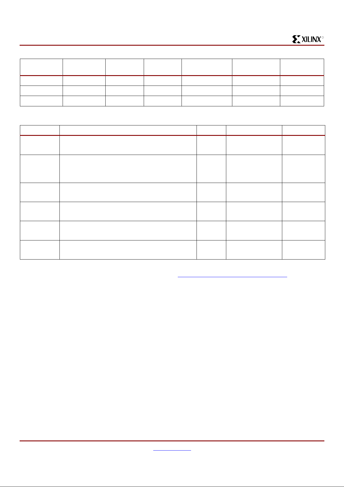
Table 1: QPro Virtex Radiation Hardened Field-Programmable Gate Array Family Members.
Device System Gates CLB Array Logic Cells
Maximum
Available I/O Block RAM Bits
Max Select
RAM Bits
XQVR300 322,970 32x48 6,912 316 65,536 98,304
XQVR600 661,111 48x72 15,552 316 98,304 221,184
XQVR1000 1,124,022 64x96 27,648 404 131,072 393,216
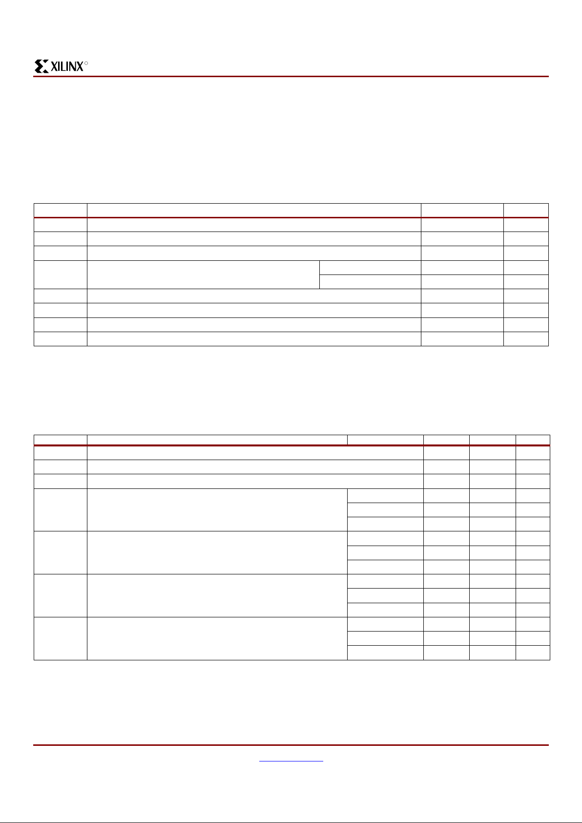
Symbol Description Min Max Units
TID Total Ionizing Dose
Method 1019, Dose Rate ~9.0 rad(Si)/sec
100 - krad(Si)
SEL Single Event Latch-up Immunity
Heavy Ion Saturation Cross Section
LET > 125 MeV cm
2
/mg
-0(cm
2
/Device)
SEU
FH
Single Event Upset CLB Flip-flop
Heavy Ion Saturation Cross Section
-6.5E – 8(cm
2
/Bit)
SEU
CH
Single Event Upset Configuration Latch
Heavy Ion Saturation Cross Section
-8.0E – 8(cm
2
/Bit)
SEU
CP
Single Event Upset Configuration Latch
Proton (63 MeV) Saturation Cross Section
-2.2E – 14 (cm2/Bit)
SEU
BH
Single Event Upset BRAM Bit
Heavy Ion Saturation Cross Section
-1.6E – 7(cm
2
/Bit)
Notes:
1. For more inf ormation, refer to " R adiation Test Results of the Virtex FPGA f or Space Based Reconfigurable Computing" and "SEU
Mitigation Techniques for Virtex FPGAs in Space Applications" at http://www.xilinx.com/products/hirel_qml.htm
.
Page 3
QPro Virtex 2.5V Radiation Hardened FPGAs
DS028 (v1.2) November 5, 2001 www.xilinx.com 3
Preliminary Product Specification 1-800-255-7778
R
Virtex Electrical Characteristics
Based on preliminary characterization. Further changes are not expected.
All specifications are representative of worst-case suppl y voltage and junction temperature c onditions. The parameters
included are common to pop ular designs and typical applications. Contact the factory for design considerations requ iring
more detailed information.
Virtex DC Characteristics
Absolute Maxim u m Rati ng s
Recommended Operating Conditions
Symbol Description Min/Max Units
V
CCINT
Supply voltage relative to GND –0.5 to 3.0 V
V
CCO
Supply voltage relative to GND –0.5 to 4.0 V
V
REF
Input reference voltage –0.5 to 3.6 V
V
IN
(3)
Input voltage relative to GND Using V
REF
–0.5 to 3.6 V
Internal threshold –0.5 to 5.5 V
V
TS
Voltage applied to 3-state output –0.5 to 5.5 V
V
CC
Longest supply voltage rise time from 1V to 2.375V 50 ms
T
STG
Storage temperature (ambient) –65 to +150 °C
T
J
Junction temperature +150 °C
Notes:
1. Stresses beyond those listed under Absolute Maximum Ratings may cause permanent damage to the device. These are stress
ratings only, and functi onal operation of the device at these o r any other c onditions beyond those l isted under Op erating Conditions
is not implied. Exposure to Absolute Maximum Ratings conditions for extended periods of time may affec t device reliability.
2. Power supplies may turn on in any order.
3. For protr acted periods (e.g. , longer than a day), V
IN
should not exceed V
CCO
by more that 3.6V.
Symbol Description Device Min Max Units
V
CCINT
Supply voltage relative to GND 2.5 – 5% 2.5 + 5% V
V
CCO
Supply voltage relative to GND 1.2 3.6 V
T
IN
Input signal transition time - 250 ns
T
IC
Initialization temperature range
(4)
XQVR300 –55 +125 °C
XQVR600 –55 +125 °C
XQVR1000 –40 +125 °C
T
OC
Operational temperature range
(5)
XQVR300 –55 +125 °C
XQVR600 –55 +125 °C
XQVR1000 –55 +125 °C
ICC
INTQ
Quiescent V
CCINT
supply current XQVR300 - 150 mA
XQVR600 - 200 mA
XQVR1000 - 200 mA
ICC
CCOQ
Quiescent V
CCO
supply current XQVR300 - 4.0 mA
XQVR600 - 4.0 mA
XQVR1000 - 4.0 mA
Notes:
1. Correct operation is guaranteed with a mi nimum V
CCINT
of 2.25V (Nomi nal V
CCINT
– 10%). Below t he minimum value stated above,
all delay parameters increase by 3% for each 50mV reduct ion in V
CCINT
below the speci fied range.
2. At junction temperatures abov e those listed as Operating Conditions, all delay par am eters increase by 0.35% per °C.
3. Input and output measurement threshold is ~50% of V
CC
.
4. Initialization occurs from the moment of V
CC
ramp-up to the rising transition of the INIT pin.
5. The device is ope rational after the INI T pin has transitioned high.
Page 4
QPro Virtex 2.5V Radiation Hardened FPGAs
4 www.xilinx.com DS028 (v1.2) Nov em ber 5, 2001
1-800-255-7778 Preliminary Product Specification
R
QPro Virtex Pinouts
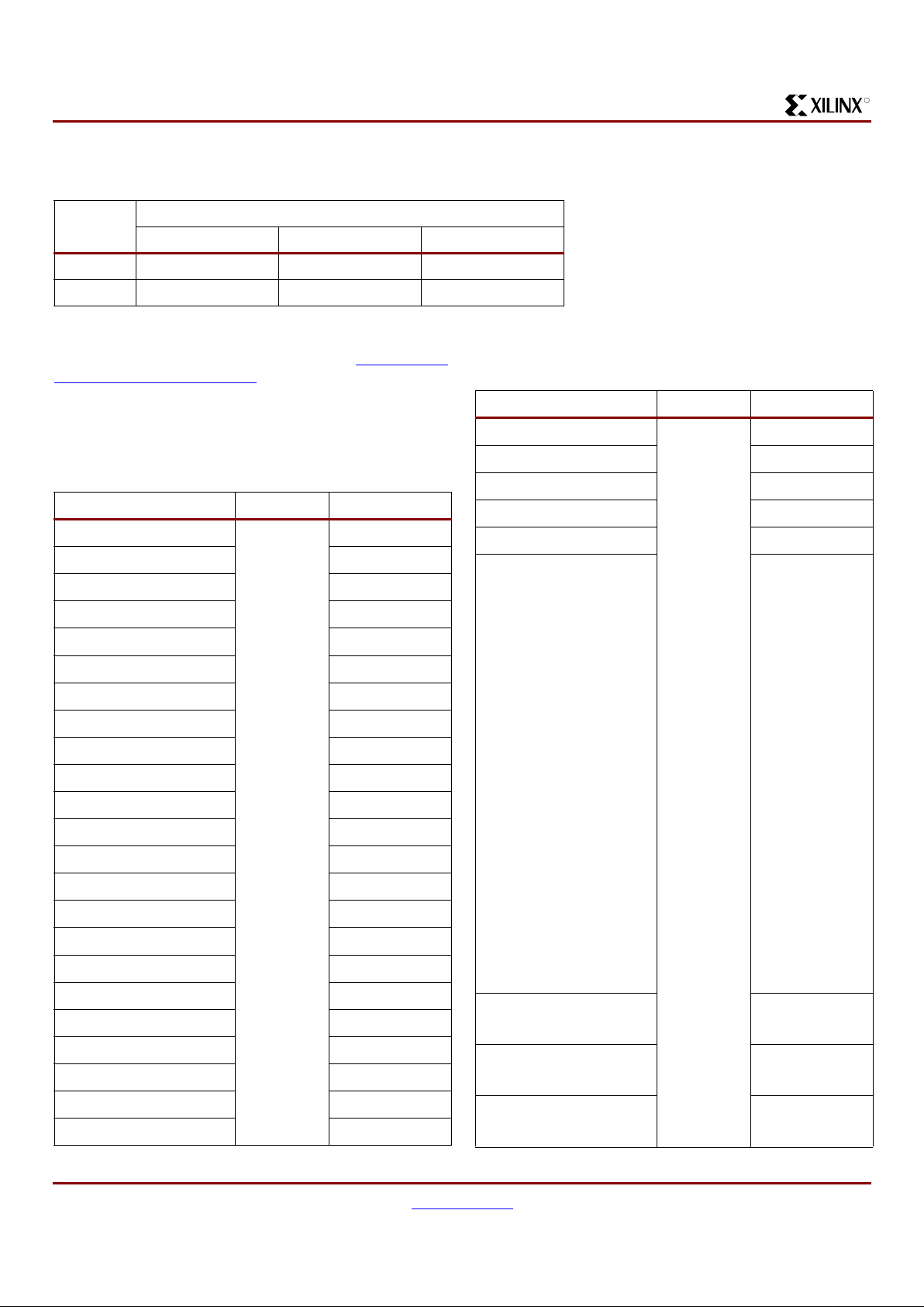
Device/Package Combinations and Maximum I/O
Pinout Tables
See the Xilinx WebLINX web site (http://www.xil-
inx.com/par tinfo/databook.htm) for updates or additional
pinout information. For convenience, Table 2 and Table 3 list
the locations of special-purpose and power-supply pins.
Pins not listed are user I/Os.
Package
Maximum User I/O (excluding dedicated clock pins)
XQVR300 XQVR600 XQVR1000
CB228 162 162 -
CG560 - - 404
Table 2: Virtex Ceramic Column Grid (CG560) Pinout
Pin Name Device CG560
GCK0 XQVR1000 AL17
GCK1 AJ17
GCK2 D17
GCK3 A17
M0 AJ29
M1 AK30
M2 AN32
CCLK C4
PROGRAM AM1
DONE AJ5
INIT AH5
BUSY/DOUT D4
D0/DIN E4
D1 K3
D2 L4
D3 P3
D4 W4
D5 AB5
D6 AC4
D7 AJ4
WRITE D6
CS A2
TDI D5
TDO XQVR1000 E6
TMS B33
TCK E29
DXN AK29
DXP AJ28
V
CCINT
(V
CCINT
pins are listed
incrementally. Connect
all pins listed for both the
required device and all
smaller devices li sted in
the same package.)
A21, B12,
B14, B18,
B28, C22,
C24, E9,
E12, F2,
H30, J1,
K32, M3,
N1, N29,
N33, U5,
U30, Y2,
Y31, AB2,
AB32, AD2,
AD32, AG3,
AG31, AJ13,
AK8, AK11,
AK17, AK20,
AL14, AL22,
AL27, AN25
V
CCO
, Bank 0 A22, A26,
A30, B19, B32
V
CCO
, Bank 1 A10, A16,
B13, C3, E5
V
CCO
, Bank 2 B2, D1,
H1, M1, R2
Table 2: Virtex C eramic Colum n Grid (C G560) Pinout
(Continued)
Pin Name Device CG560
Page 5
QPro Virtex 2.5V Radiation Hardened FPGAs
DS028 (v1.2) November 5, 2001 www.xilinx.com 5
Preliminary Product Specification 1-800-255-7778
R
V
CCO
, Bank 3 XQVR1000 V1, AA2,
AD1, AK1, AL2
V
CCO
, Bank 4 AM2, AM15,
AN4, AN8,
AN12
V
CCO
, Bank 5 AL31, AM21,
AN18, AN24,
AN30
V
CCO
, Bank 6 W32, AB33,
AF33, AK33,
AM32
V
CCO
, Bank 7 C32, D33,
K33, N32, T33
V
REF
, Bank 0
Within each bank, if input
reference voltage is not
required, all V
REF
pins
are general I/O.
A19, D20,
D26, D29,
E21, E23,
E24, E27,
V
REF
, Bank 1
Within each bank, if input
reference voltage is not
required, all V
REF
pins
are general I/O.
A6, D7 ,
D10, D11,
D13, D16,
E7, E15
V
REF
, Bank 2
Within each bank, if input
reference voltage is not
required, all V
REF
pins
are general I/O.
B3, G5,
H4, K5,
L5, N5,
P4, R1
V
REF
, Bank 3
Within each bank, if input
reference voltage is not
required, all V
REF
pins
are general I/O.
V4, W5,
AA4, AD3,
AE5, AF1,
AH4, A K2
V
REF
, Bank 4
Within each bank, if input
reference voltage is not
required, all V
REF
pins
are general I/O.
AK13 , AL7,
AL9, AL10,
AL16, AM4,
AM14,AN3
V
REF
, Bank 5
Within each bank, if input
reference voltage is not
required, all V
REF
pins
are general I/O.
AJ18, AJ25,
AK28, AL20,
AL24, AL29,
AM26, AN23
Table 2: Virtex Ceramic Column Grid (CG560) Pinout
(Continued)
Pin Name Device CG560
V
REF
, Bank 6
Within each bank, if input
reference voltage is not
required, all V
REF
pins
are general I/O.
XQVR1000 V29, Y32,
AA30,AD31,
AE29, AK32,
AE31, AH30
V
REF
, Bank 7
Within each bank, if input
reference voltage is not
required, all V
REF
pins
are general I/O.
D31, E31,
G31, H32,
K31, P31,
T31, L33
GND A1, A7, A12,
A14, A18, A20,
A24, A29,
A32, A33,
B1, B6,
B9, B15,
B23, B27,
B31, C2 ,
E1, F32,
G2, G33,
J32, K1,
L2, M33,
P1, P33,
R32, T1,
V33, W2,
Y1, Y33,
AB1, AC32,
AD33, AE2,
AG1, AG3 2,
AH2, AJ33,
AL32, AM3,
AM7, AM11,
AM19, AM25,
AM28, AM33,
AN1, AN2,
AN5, AN10,
AN14, AN16,
AN20, AN22,
AN27, AN33
No Connect XQVR1000 C31, AC2, AK4,
AL3
Table 2: Virtex C eramic Colum n Grid (C G560) Pinout
(Continued)
Pin Name Device CG560
Page 6

QPro Virtex 2.5V Radiation Hardened FPGAs
6 www.xilinx.com DS028 (v1.2) Nov em ber 5, 2001
1-800-255-7778 Preliminary Product Specification
R
Table 3: CQFP Package (CB228)
Function Pin # Bank #
GND 1 7
TMS 2
IO 3
IO 4
IO_VREF_7 5
IO 6
IO 7
GND 8
IO 9
IO 10
IO 11
IO_VREF_7 12
IO 13
GND 14
V
CCINT
15
IO 16
IO 17
V
CCO
18
IO 19
IO 20
IO_VREF_7 21
IO 22
IO 23
IO 24
IO 25
IO_IRDY 26
GND 27
V
CCO
28 6
IO_TRDY 29
V
CCINT
30
IO 31
IO 32
IO 33
IO_VREF_6 34
IO 35
IO 36
V
CCO
37
IO 38
IO 39
IO 40
V
CCINT
41
GND 42
IO 43
IO_VREF_6 44
IO 45
IO 46
IO_VREF_6 47
GND 48
IO 49
IO 50
IO_VREF_6 51
IO 52
IO 53
IO 54
M1 55
GND 56
M0 57
Table 3: CQFP Package (CB228) (Continued)
Function Pin # Bank #
Page 7

QPro Virtex 2.5V Radiation Hardened FPGAs
DS028 (v1.2) November 5, 2001 www.xilinx.com 7
Preliminary Product Specification 1-800-255-7778
R
V
CCO
58 5
M2 59
IO 60
IO 61
IO 62
IO_VREF_5 63
IO 64
IO 65
GND 66
IO_VREF_5 67
IO 68
IO 69
IO_VREF5 70
IO 71
GND 72
V
CCINT
73
IO 74
IO 75
V
CCO
76
IO 77
IO 78
IO_VREF_5 79
IO 80
IO 81
IO 82
Table 3: CQFP Package (CB228) (Continued)
Function Pin # Bank #
V
CCINT
83 4
GCK1 84
VCCO 85
GND 86
GCKO 87
IO 88
IO 89
IO 90
IO 91
IO_VREF_4 92
IO 93
IO 94
V
CCO
95
IO 96
IO 97
IO 98
V
CCINT
99
GND 100
IO 101
IO_VREF_4 102
IO 103
IO 104
IO_VREF_4 105
GND 106
IO 107
IO 108
IO_VREF_4 109
IO 110
IO 111
IO 112
GND 113
DONE 114
V
CCO
115
Table 3: CQFP Package (CB228) (Continued)
Function Pin # Bank #
Page 8

QPro Virtex 2.5V Radiation Hardened FPGAs
8 www.xilinx.com DS028 (v1.2) Nov em ber 5, 2001
1-800-255-7778 Preliminary Product Specification
R
PROGRAM 116 3
IO_INIT 117
IO_D7 118
IO 119
IO_VREF_3 120
IO 121
IO 122
GND 123
IO_VREF_3 124
IO 125
IO 126
IO_VREF_3 127
IO_D6 128
GND 129
V
CCINT
130
IO_D5 131
IO 132
V
CCO
133
IO 134
IO 135
IO_VREF_3 136
IO_D4 137
IO 138
IO 139
V
CCINT
140
IO_TRDY 141
V
CCO
142
Table 3: CQFP Package (CB228) (Continued)
Function Pin # Bank #
GND 143 2
IO_IRDY 144
IO 145
IO 146
IO 147
IO_D3 148
IO_VREF_2 149
IO 150
IO 151
V
CCO
152
IO 153
IO 154
IO_D2 155
V
CCINT
156
GND 157
IO_D1 158
IO_VREF_2 159
IO 160
IO 161
IO_VREF_2 162
GND 163
IO 164
IO 165
IO_VREF_2 166
IO 167
IO_DIN_D0 168
IO_DOUT_BUSY 169
CCLK 170
V
CCO
171
Table 3: CQFP Package (CB228) (Continued)
Function Pin # Bank #
Page 9

QPro Virtex 2.5V Radiation Hardened FPGAs
DS028 (v1.2) November 5, 2001 www.xilinx.com 9
Preliminary Product Specification 1-800-255-7778
R
TDO 172 1
GND 173
TDI 174
IO_CS 175
IO_WRITE 176
IO 177
IO_VREF_1 178
IO 179
GND 180
IO_VREF_1 181
IO 182
IO 183
IO_VREF_1 184
IO 185
GND 186
V
CCINT
187
IO 188
IO 189
IO 190
V
CCO
191
IO 192
IO 193
IO_VREF_1 194
IO 195
IO 196
IO 197
IO 198
GCK2 199
GND 200
V
CCO
201
Table 3: CQFP Package (CB228) (Continued)
Function Pin # Bank #
GCK3 202 0
V
CCINT
203
IO 204
IO 205
IO 206
IO_VREF_0 207
IO 208
IO 209
V
CCO
210
IO 211
IO 212
IO 213
V
CCINT
214
GND 215
IO 216
IO_VREF_0 217
IO 218
IO 219
IO_VREF_0 220
GND 221
IO 222
IO 223
IO_VREF_0 224
IO 225
IO 226
TCK 227
V
CCO
228
Table 3: CQFP Package (CB228) (Continued)
Function Pin # Bank #
Page 10

QPro Virtex 2.5V Radiation Hardened FPGAs
10 www.xilinx.com DS028 (v1.2) November 5, 2001
1-800-255-7778 Preliminary Product Specification
R
Pinout Diagrams
The following diagrams illustrate the locations of special-purpose pins on Virtex FPGAs. Table 4 lists the symbols used in these diagrams. The diagrams also show
I/O-bank boundaries.
GND 1, 8, 14, 27, 42,
48, 56, 66, 72,
86, 100, 106,
113, 123, 129,
143, 157, 163,
173, 180, 186,
200, 215, 221
-
V
CCINT
15, 30, 41, 73,
83, 99, 130,
140, 156, 187,
203, 214
-
V
CCO
18, 28, 37, 58,
76, 85, 95, 115,
133, 142, 152,
171, 191, 201,
210, 228
-
Table 4: Pinout Diagram Sym bols
Symbol Pin Funct i on
S General I/O
d Device-dependent general I/O, n/c on
smaller devices
VV
CCINT
Table 3: CQFP Package (CB228) (Continued)
Function Pin # Bank #
v Device-dependent V
CCINT
, n/c on smaller
devices
OV
CCO
RV
REF
r Device-dependent V
REF
, rema i n s I/O on
smaller devices
G Ground
Ø, 1, 2, 3 Global Clocks
❿, ❶, ❷ M0, M1, M2
➉, ➀, ➁, ➂,
➃, ➄, ➅, ➆
D0/DIN, D1, D2, D3, D4, D5, D6, D7
BDOUT/BUSY
DDONE
PPROGRAM
IINIT
K CCLK
WWRITE
SCS
T Boundary-scan test access port
+ Tempera ture diode, anode
– Tem perature diode, cathode
n No connect
Table 4: Pino ut D iag ram Symbols (Continued)
Symbol Pin Funct ion
Page 11

QPro Virtex 2.5V Radiation Hardened FPGAs
DS028 (v1.2) November 5, 2001 www.xilinx.com 11
Preliminary Product Specification 1-800-255-7778
R
CG560 Pin Functi on Diag ra m
1
2
3
4
5
6
7
8
9
10
11
12
13
14
15
16
17
18
19
20
21
22
23
24
25
26
B
C
D
E
F
G
H
J
K
L
M
N
P
R
T
U
V
W
Y
AA
AB
AC
AD
AE
AF
A
K
T
➆
–
I
+
Ø
O
1
❶
B
➀
➁
➃
➄
➅
❿
B
C
D
E
F
G
H
J
K
L
M
N
P
R
T
U
V
W
Y
AA
AB
AC
AD
AE
AF
A
1
2
3
4
5
6
7
8
9
10
11
12
13
14
15
16
17
18
19
20
21
22
23
24
25
26
➉
Bank 1 Bank 0
Bank 4
Bank 6
Bank 5
Bank 3
Bank 7Bank 2
CG560
(Top View)
W
27
28
29
30
31
32
33
27
28
29
30
31
32
33
AG
AH
AJ
AK
AL
AM
AN
AG
AH
AJ
AK
AL
AM
AN
✳✳✳ ✳✳✳✳✳ ✳✳✳✳ ✳
✳✳ ✳✳ ✳✳ ✳✳ ✳✳✳ ✳✳✳ ✳✳
✳ ✳✳✳✳✳✳✳✳✳✳✳✳✳✳✳✳✳ ✳ ✳✳✳✳✳✳ ✳
✳✳ ✳✳ ✳ ✳✳ ✳✳ ✳✳✳✳✳ ✳✳ ✳ ✳
✳✳ ✳✳✳✳✳✳✳✳✳✳✳ ✳✳✳✳ ✳✳
✳✳✳ ✳✳✳✳✳✳✳ ✳✳✳ ✳✳✳✳✳✳ ✳✳ ✳✳✳
✳ ✳✳✳ ✳✳ ✳ ✳✳✳ ✳✳ ✳✳✳✳✳✳✳ ✳
✳ ✳✳✳✳ ✳✳✳✳ ✳✳✳✳✳✳✳✳ ✳
✳✳ ✳✳✳ ✳✳ ✳✳✳ ✳ ✳✳✳ ✳ ✳✳✳
✳✳✳✳✳✳✳✳✳ ✳✳✳✳
✳ ✳✳✳
✳✳✳
✳✳ ✳
✳✳✳✳
✳✳
✳✳
✳✳✳
✳✳✳
✳✳
✳✳✳
✳✳✳✳
✳✳✳✳
✳✳ ✳
✳✳
✳✳✳
✳✳✳
✳
✳✳✳
✳
✳✳
✳✳✳
✳✳✳✳
✳✳✳
✳✳
✳✳✳ ✳
✳✳ ✳
✳✳✳
✳✳✳ ✳
✳✳
✳✳✳✳
✳✳✳✳
✳✳
✳✳ ✳
✳✳✳ ✳
✳✳ ✳
✳ ✳✳✳
✳✳✳
✳✳✳ ✳
✳✳
✳ ✳✳✳
✳✳✳
✳✳✳ ✳
✳✳
✳✳✳
✳✳✳✳
✳✳ ✳
✳ ✳✳✳
R
OR
O
G
O
GGRGOGP
RV
V
GR
RVG
G
RR
G
R
G
n
OR
OVR
R
V
n
R
O
GO
O
GG
G
O
G
O
O
V
VG
OV R
OG
G
❷
OGGGO
V
GV
GVO
R
G
GG
R
GS RG OGGO3GGR VO G O GO GG
GO G G
v
VOGVOGGVGOT
GO V
n
O
OTRR R2R R
R
O
GOT
r
VVR R R
V G
GR RG
OR V
V G
G RVO
GR
O G
V OV
G
➂
RRG
OR G
G RO
VV
OR R G
GR O
GV VRG
D
n
v
v
v
v
v
v
v
rr
rr
rr
r
r
r
r
r
r
r
r
r
r
r
r
r
r
r
r
r
Page 12

QPro Virtex 2.5V Radiation Hardened FPGAs
12 www.xilinx.com DS028 (v1.2) November 5, 2001
1-800-255-7778 Preliminary Product Specification
R
Package Drawing CG560 Ceramic Column Grid
DS028_01_011900
Page 13

QPro Virtex 2.5V Radiation Hardened FPGAs
DS028 (v1.2) November 5, 2001 www.xilinx.com 13
Preliminary Product Specification 1-800-255-7778
R
Device/Package Combinations and Maximum I/O
Ordering Information
Package
Maximum User I/O (excluding dedicated clock pins)
XQVR300 XQVR600 XQVR1000
CB228 162 162 CG560 - - 404
XQVR1000 -4 CG 560 V
Example:
Manufacturing Grade
Number of Pins
Package Type
Device Type
Speed Grade
(1)
Device Ordering Options
Device Type Packa ge Grade
XQVR300 CB228 228-pin Ceramic Quad Flat Package
M
Military Ceramic TC = –55°C to +125°C
XQVR600 CG560 560-column Ceramic Column Grid Package
V
QPro Plus TC = –55°C to +12 5°C
XQVR1000 Q MIL-PRF-38535
(2)
TC = –55°C to +125°C
Notes:
1. -4 only supported speed grade.
2. Class Q must be ordered with SMD number.
Device Ordering Combinations
M Grade V Grade
XQVR300-4CB228M XQVR300-4CB228V
XQVR600-4CB228M XQVR600-4CB228V
XQVR1000-4CG560M XQVR1000-4CG560V
Page 14

QPro Virtex 2.5V Radiation Hardened FPGAs
14 www.xilinx.com DS028 (v1.2) November 5, 2001
1-800-255-7778 Preliminary Product Specification
R
SMD (Class Q) Oderin g Optio ns
Revision History
The following table shows the revision history for this document.
Date Version Revision
04/25 /00 1.0 Init ia l X ilin x r ele as e .
02/13/01 1.1 Upda ted TemperatureSpecifications.
11/05/01 1.2 Upda ted Temp specifications for V600, Added Class V option and SMD. Updated format.
5962 R 9957201 Q Y C
Lead Finish
Generic Standard
Microcircuit Drawing (SMD)
Device Type
Package Type
QML Certified MIL-PRF-3 8535
Valid SMD Combinations
SMD Number Device Pkg Marki ng s Lead Finish
5962R9957201QYC
XQVR300-4CB228Q Lid Gold Plate
5962R9957201QZC XQVR300-4CB228Q Base Gold Plate
5962R9957301QYC XQVR600-4CB228Q Lid Gold Plate
5962R9957301QZC XQVR600-4CB228Q Base Gold Plate
5962R9957401QXC XQVR1000-4CG560Q - Solder Column
Radiation Hardened
 Loading...