

Page 1
FEATURES
■ Low power consumption
■ 2.5GHz input
■ 144 frequencies, 1MHz steps (20MHz crystal)
■ Forms complete phase locked loop using external
VCO and loop components
■ Serially programmed via 3 wire bus
■ Contains anti-modulation circuit
■ Part of DE6038 Chip-set (WL600C, WL102)
ORDERING INFORMATION
WL800/KG/TP1R
The WL800 is a low power single chip frequency synthesiser.
The circuit is fabricated on Mitel Semiconductor HG process
and operates from a supply voltage of 2.7 - 3.6V. It is designed
to work with the Mitel Semiconductor WL600C RF and IF
circuit and the WL102 WLAN controller chip which together
make up the DE6038 frequency hopping Wireless Local Area
Network (WLAN) transceiver.
RELATED DOCUMENTS
WL600C, WL102 datasheets
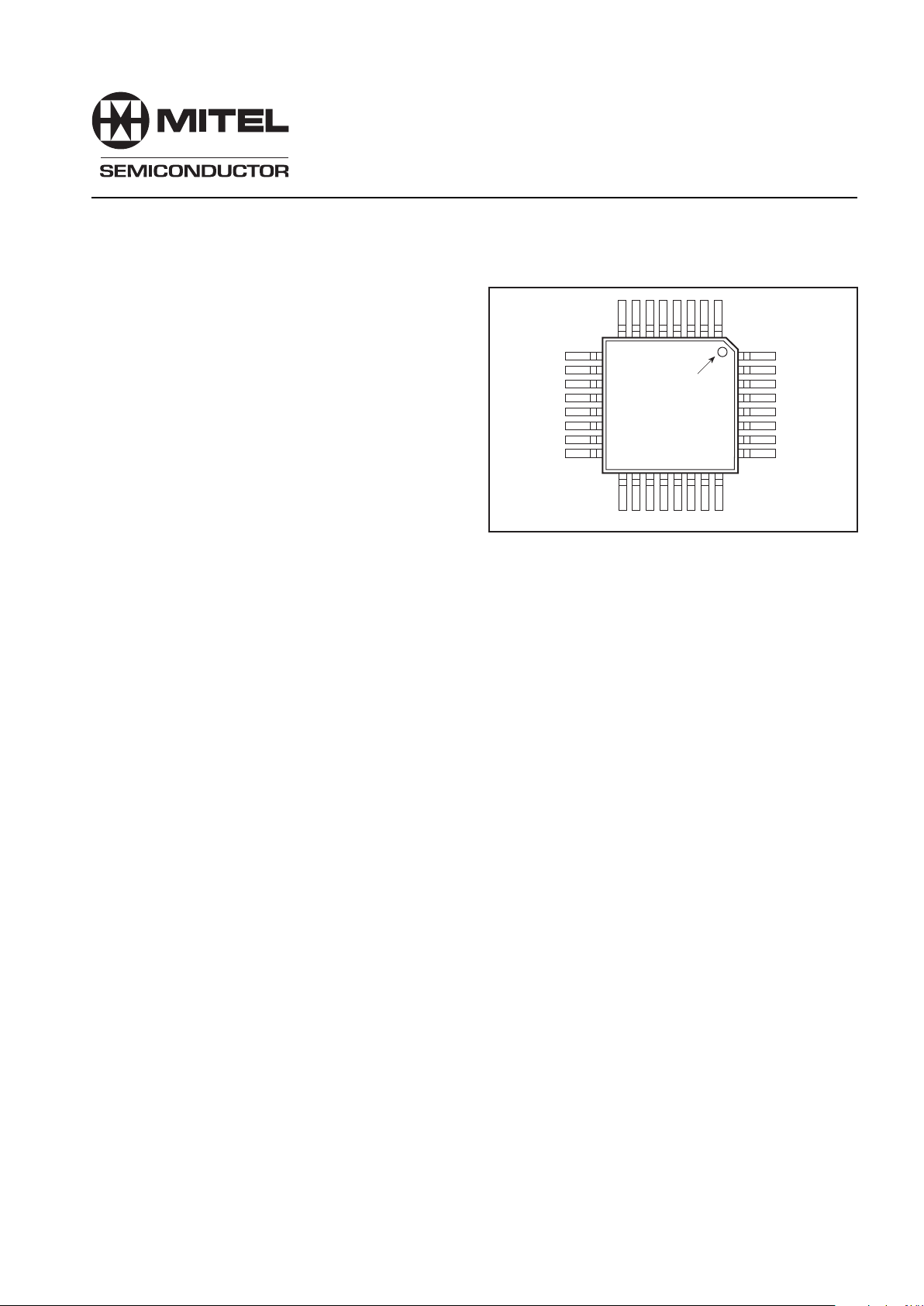
TQFP 32
Fig.1 Pin connections - top view
PIN 1 IDENT
ABSOLUTE MAXIMUM RATINGS
Supply Voltage Vcc 4VDC
Transmit/Receive and -0.5VDC to Vcc +0.5VDC
Standby Input
Prescaler Inputs Pins 30 &31 No DC. Externally Capacitively
Coupled.
Output Current (any output) TBD mA
Junction temperature Tj 150°C
ESD protection: 2kV
Operating temperature -20 to +85°C
WL800
2.5GHz Frequency Synthesiser
Preliminary Information
DS4583 1.6 October1997
Page 2

2
WL800
PIN REFERENCE TYPE DESCRIPTION
1 VCC1 VCC Power for serial data bus
2 CS-DATA IN Channel Data in (Synth Programming)
3 CS-CLK IN Data Clock (Synth Programming)
4 CS-LOADB IN Data Enable (Synth Programming)
5 STDBYB IN Power down control Active = Logic 1 Standby = logic 0
6 VEE1 GND Ground connection
7 ISET Set modulation current
8 ICP Set charge pump current
9 VEE3 GND Ground connection
10 TXD IN Modulation data in
11 COM CAP Compensation capacitor for modulation data
12 RCOMP OUT Resistor for V/I converter
13 IDOUT OUT Modulation data out
14 TXRXB IN Transmit/Receive control Transmit = Logic 1 Receive = Logic 0
15 VARICAP OUT Control V to varicap in VCO
16 VCC3 VCC Power for charge pump and loop amplifier and modulator
17 LOOPFILTER OUT Loop filter out (Loop Filter Components)
18 CPUMPREF Charge pump reference voltage
19 CPUMPOUT OUT Charge pump out (Loop Filter Components)
20 VEE2 GND Ground connection
21 SYSCLK OUT Reference (system) clock out
22 XTAL Crystal connection (Differential)
23 XTALB Crystal connection (Differential)
24 VCC2 VCC Power for reference oscillator
25 FREF OUT Reference frequency monitor
26 LKCAP Lock detect capacitor
27 LCKDETB OUT Lock detect output
28 FV OUT VCO frequency / (NM+A) monitor
29 VEE5 GND Ground connection
30 VCC VCC Power for prescaler, AM counter Ref divider, phase detector and
lock detector
31 VCOIPB IN Prescaler IN32 VCOIP IN Prescaler IN+
DEVICE PIN OUT
Page 3
3
WL800
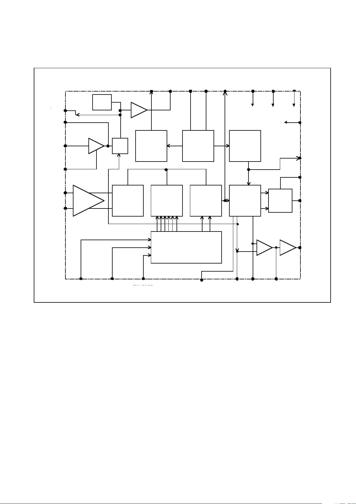
PRE-SCALER A COUNTER
PHASE DET
& CHARGE
PUMP
INPUT REGISTER
M COUNTER
REFERENCE
OSC
DIVIDE
BY 20
REF OUT
BUFFER
LOCK
DETECT
PRE
AMP
DATA
BUFFER
1,16,24,30
Vcc
6,9,20,29
Vee
STANDBY
5
14
TXRXB
DATA
2
CLK
3
ENABLEB
4
VCOIP
32
VCOIPB
31
DIN
10
IDOUT
13
ISET
7
21
REF
OUT
23
XTAL122XTAL2
LKCAP
26
LKDETB
27
CPUMP
REF
18
VARICAP
15
LOOP
FILTER
17
CPUMP
OUT
19
MOD
COMP
COMP
11
ICP
8
FREF
25
28
FV
12
RCOMP
VCAP
CHARGE
CAP
BUFFER
1/3
SYSCLK
STDBYB
LCKDETB
COMPCAP
TXD
CS-DATA CS-CLK
CS-LOADB
B
Fig. 1 WL800 block diagram
XTALB
Page 4
4
WL800
ELECTRICAL CHARACTERISTICS
These characteristics are guaranteed over the following conditions (unless otherwise stated):
T
AMB
= -20°C, to +85°C, Vcc = 2.7V to 3.6V
Characteristic Value Unit Condition
MIN TYP MAX
Supply current (total)
Transmit 37 50 mA
Receive 35 50 mA
Supply current in standby 3 5 mA
PROGRAMMING INPUTS
Logic low voltage 0 0.4 V
Logic high voltage 0.8Vcc Vcc V
Input current 1 µA Input level high
Data clock frequency (1/tclock) 20 MHz See Fig. 2
Data/Enable set up time (t set up) 10 ns See Fig. 2
Enable hold time (t enable) 10 ns See Fig. 2
Positive clock pulse width (tp) 20 ns See Fig. 2
Negative clock pulse width (t neg) 20 ns See Fig. 2
STANDBY INPUT
Logic low input voltage 0 0.8 V Circuit powered down
Logic high input voltage Vcc -0.7 Vcc V Circuit powered up
Input current 100 150 µA Circuit powered up
-150 µA Circuit powered down
Standby to operate time 3 µs *References operational (see note 1)
TX/RX INPUT
Logic low input voltage 0 0.8 V Receive mode
Logic high input voltage Vcc -0.7 Vcc V Transmit mode
Input current 10 µA
REFERENCE OUTPUT
Reference output frequency 20 MHz With 20MHz crystal
Reference clock output voltage 200 250 300 mVp-p With 15pF load
Reference output impedance 600 Ohms
Mark Space ratio -2% 50/50 +2% With 15pF load
Rise time 15 ns
Fall time 15 ns
Crystal Drive Levels required 200 mV Pins 22,23 differential
Page 5

5
WL800
ELECTRICAL CHARACTERISTICS (continued)
These characteristics are guaranteed over the following conditions (unless otherwise stated):
T
AMB
= -20°C, to +85°C, Vcc = 2.7V to 3.6V
Characteristic Value Unit Condition
MIN TYP MAX
LOCK DETECT CIRCUIT
Smoothing capacitor charge/ 80 110 150 µA Determined by application.
discharge current
Threshold voltage Vcc-0.3 V On smoothing capacitor
Output high voltage 1.8 Vcc V I out = 10µA
Output low voltage Vee 0.5 V I out = 0 µA
PHASE DETECTOR AND
CHARGE PUMP
Comparison frequency 1 MHz Divided crystal reference
Charge pump output current ±1 mA Rpin 8 = 10k
Up down current matching 5 %
Reference voltage V
cc-1.05 Vcc-0.7 V
CHARGE PUMP OP-AMP
First Stage:
High output voltage 2.4 V
Low output voltage 0.3 V
Second Stage:
Filter drive amplifier output current ±1mA
Filter drive amp output swing 0.77 Vp-p
PRESCALER
Input drive voltage 40 200 mV rms
Maximum operating frequency 3 GHz
Input Impedance 330Ω
0.5pF
TRANSMIT DATA INPUT
Logic low -60 -100 µA Rsource=20k
Logic high +60 +100 µA
TX DATA OUT
Logic 0 output current 25 50 100 µA Set by external resistor on pin 7
Logic 1 output current 200 nA Leakage Current
Output current in receive mode 25 µA Equal to 0.5 mod current
Page 6

6
WL800
ELECTRICAL CHARACTERISTICS (continued)
These characteristics are guaranteed over the following conditions (unless otherwise stated):
T
AMB
= -20°C, to +85°C, Vcc = 2.7V to 3.6V
Characteristic Value Unit Condition
MIN TYP MAX
MOD. CURRENT INPUT
Mod current set pin current 25 µA Set by external resistor on pin 7.
R = 47k
COMPENSATION CAP PIN
Compensation current -25 µA Set by external resistor on
pin 7. R=47k.
Compensation current matching 2 % Compensation capacitor 8.2nF
Compensation capacitor voltage CPRef - CPRef CPRef V Receive mode
0.02 +0.02
Compensation capacitor voltage 88 98 +110 mV 1 MHz data, 32bits ‘0’
-120 -98 -88 mV 1 MHz data, 32bits ‘1’
VCAP CHARGE
Settling Time 100 µs Receive mode
Charging Current 20 mA Receive mode.
Vcap initially at 0 V.
Offset Voltage 15 mV Receive mode.
COMPENSATION VtoI
(CAPBUFFER+RCOMP)
Compensation current into Loop +52.08 nA Per 1us of databit 0
Filter -52.08 nA Per 1us of databit 1
Max. Compensation current 1.666 mA for 32 bits(1) at 1MHz
CAPACITOR BUFFER
Offset Voltage 15 mV
External Resistor RCOMP 58000 Ohms
Note: 1. Standby to operate time refers to the time for internal current references to become operational.
Page 7

7
WL800
FUNCTIONAL DESCRIPTION
Reference Frequency
The reference frequency is generated using a 20MHz
crystal in conjunction with an on chip oscillator maintaining
circuit. A buffer circuit provides a low level voltage output
signal at the crystal frequency to drive the logic in the protocol
and control chip. The crystal frequency is divided by 20 to
provide the reference signal to the phase comparator.
Counters / Dividers
An external oscillator is used to feed the input of the
preamplifier in the synthesiser, (this isolates the counters from
the oscillator and reduces the level of drive signal required by
the synthesiser). The output of the preamplifier drives a dual
modulus prescaler with ratios of 48/49, which in turn then
drives the standard A-M counter arrangement. The A counter
then provides the modulus control signal back to the
prescaler. The counter system has an overall division ratio
given by the formula MN+A where N is the lower divide ratio
of the prescaler (48).
The divide ratio of the M and A counters is programmable
to allow the oscillator to be tuned over the required frequency
range of 144 channels at 1MHz spacing. The M count ratio can
be programmed over the range 49 to 52 and the A counter from
1 to 48 giving a total divide ratio from 2353 to 2544 which is
greater than necessary to tune the required frequency range.
Programming
The programming data for the synthesiser is entered via a
three wire serial data bus consisting of Enable, Clock and Data
signals.
The enable signal is taken low at the start of the programming sequence and remains low for the duration of the 8 serial
data bits. A positive clock edge is required to strobe each data
bit into the input register. When all 8 data bits are entered, the
enable pin is taken high forcing the counters to zero and
preloading the new count data when the counter is next
clocked . The charge pump is disabled for a short period after
the enable pin goes low to prevent glitch energy being transferred to the VCO.
Phase Detectors
A conventional digital phase frequency detector incorporating dead band suppression is used in conjunction with a
charge pump to steer the VCO. An internal op-amp maintains
the charge pump pin at the same voltage as the charge pump
reference by virtual earth principles. The op-amp is split into
two parts with the first section having a relatively low current
drive capability but including the high gain stages of the
amplifier. The second stage has a controlled voltage gain of
1/3 but high input impedance and low output impedance. This
minimises loading to the high output impedance of the first
stage and provides sufficient drive current via the loop filter to
maintain virtual earth at the charge pump output. The output
from the first stage is designed to swing close to the positive
and negative rails so as to provide maximum voltage swing to
the varactor controlling the VCO. A compensating capacitor
can be connected to this point to stabilise the amplifier.
A lock detect output (active low) is provided to give an
indication to the controller that the phase locked loop is locked,
preventing transmission on illegal frequencies.
Antimodulation
The WL800 contains a data buffer circuit which accepts
transmit data from the CMOS controller circuit and converts
the CMOS input to a tristate current output for driving the
transmit spectrum shaping filter. The buffer gives zero current
for a logic “1” input, a high current (+2I) for a logic “0” and a
current midway between the two (+I) for use during the
transmit amplifier power up/down period and during receive.
This function prevents the synthesiser centring its frequency
on either a logic “1” or “0” and removes the possibility of overmodulation at the start of a transmission. The amplitude of the
output current and therefore modulation index of the radio is
controlled by an external resistor connected to ground.
A data compensation path is included which counteracts the
tendency of the PLL to drift back to centre frequency when the
data is non-white. This is achieved by charging an external
capacitor with a current +I when data is low, and discharging
it by a current -I when data is high. The capacitor voltage,
which then represents an integrated form of the data is
converted to a current via a buffer and an external resistor
(RCOMP), and fed into the Loop Filter in addition to the Phase
Detector output. During Receive Mode, the capacitor is
charged to the Charge Pump Reference voltage.
Page 8

8
WL800
WL800 PROGRAMMING
Frequency A counter M counter 6 bit binary A bit binary M
MHz Value Value Value d0-d5 Value d6-d7
2357 5 49 101000 00
2358 6 49 011000 00
2400 48 49 000011 00
2401 1 50 100000 10
2448 48 50 000011 10
2449 1 51 100000 01
2496 48 51 000011 01
2497 1 52 100000 11
2498 2 52 010000 11
2499 3 52 110000 11
2500 4 52 001000 11
Notes: 1.The binary data is in reverse order.
2.The data is programmed with bit d7 first and d0 last
d0 d1 d2 d3 d4 d5 d6 d7
A counter M counter
DATA
CLOCK
DATA
ENABLE
t set up
t enable
t clock
tp
t neg
TIMING DIAGRAM
Fig. 2 Timing diagram
CS_LOADB
CS_DATA
CS_CLK
Page 9

9
WL800
CONTROL SIGNALS
Control Line Logic ‘0’ Logic ‘1’
STDBYB Standby Active
TXRXB Receive Transmit
LCKDETB Locked Unlocked
Page 10

Page 11

M Mitel (design) and ST-BUS are registered trademarks of MITEL Corporation
Mitel Semiconductor is an ISO 9001 Registered Company
Copyright 1999 MITEL Corporation
All Rights Reserved
Printed in CANADA
TECHNICAL DOCUMENTATION - NOT FOR RESALE
World Headquarters - Canada
Tel: +1 (613) 592 2122
Fax: +1 (613) 592 6909
North America Asia/Pacific Europe, Middle East,
Tel: +1 (770) 486 0194 Tel: +65 333 6193 and Africa (EMEA)
Fax: +1 (770) 631 8213 Fax: +65 333 6192 Tel: +44 (0) 1793 518528
Fax: +44 (0) 1793 518581
http://www.mitelsemi.com
Information relating to products and services furnished herein by Mitel Corporation or its subsidiaries (collectively “Mitel”) is believed to be reliable. However, Mitel assumes no
liability for errors that may appear in this publication, or for liability otherwise arising from the application or use of any such information, product or ser vice or for any infringement of
patents or other intellectual property rights owned by third parties which may result from such application or use. Neither the supply of such information or purchase of product or
service conveys any license, either express or implied, under patents or other intellectual property rights owned by Mitel or licensed from third parties by Mitel, whatsoever.
Purchasers of products are also hereby notified that the use of product in certain ways or in combination with Mitel, or non-Mitel furnished goods or services may infringe patents or
other intellectual property rights owned by Mitel.
This publication is issued to provide information only and (unless agreed by Mitel in writing) may not be used, applied or reproduced for any purpose nor form par t of any order or
contract nor to be regarded as a representation relating to the products or services concerned. The products, their specifications, services and other information appearing in this
publication are subject to change by Mitel without notice. No warranty or guarantee express or implied is made regarding the capability, performance or suitability of any product or
service. Information concerning possible methods of use is provided as a guide only and does not constitute any guarantee that such methods of use will be satisfactory in a specific
piece of equipment. It is the user’s responsibility to fully determine the performance and suitability of any equipment using such information and to ensure that any publication or
data used is up to date and has not been superseded. Manufacturing does not necessarily include testing of all functions or parameters. These products are not suitable for use in
any medical products whose failure to perform may result in significant injury or death to the user. All products and materials are sold and services provided subject to Mitel’s
conditions of sale which are available on request.
 Loading...