

Datasheet W6PXD3O-0000, W6NXD3L-0000, W6NXD3K-0000, W6NXD3J-0000, W6NXD0KLSR-0000 Datasheet (CREE)
...Page 1

Effective December 1998 • Revised March 2003 • Page 1
Silicon Carbide
Substrates
Product Specifications
4H Silicon Carbide
(n/p-type)
6H Silicon Carbide
(n/p-type)
Page 2
Page 2 • Effective December 1998 • Revised March 2003
Properties and Specifications for
Silicon Carbide
Applications: • High Frequency Power Devices
• High Power Devices
• High Temperature Devices
• Optoelectronic Devices
• III-V Nitride Deposition
Physical Properties
Polytype Single Crystal 4H Single Crystal 6H
Crystal Structure Hexagonal Hexagonal
Bandgap 3.26 eV 3.03 eV
Thermal Conductivity
(Typical Range)
3.0-3.8 W/cm • K @ 298K
(2.3-2.8 W/cm • K @ 373K)
3.0-3.8 W/cm • K @ 298K
(2.3-2.8 W/cm • K @ 373K)
Lattice Parameters
a=3.073 Å
c=10.053Å
a=3.081 Å
c=15.117Å
Mohs Hardness ~9 ~9
Page 3
Effective December 1998 • Revised March 2003 • Page 3
Product Descriptions
Part Number Options
W X X X X X X - X X X X
0 = No Epitaxy
1 = 1 Layer
2 = 2 Layer
3 = 3 Layer
4 = 4 Layer
5 = 5 Layer
0 = No Epitaxy
S = Standard SiC Epitaxy
T = Thick SiC Epitaxy
0 = Single Side Polish, Si Face Epi Ready
C = Single Side Polish, C Face Epi Ready
D = Double Side Polish, Si Face Epi Ready
G = Double Side Polish, C Face Epi Ready
1 = CMP Polish, Si Face Epi Ready
2 = Double Side CMP Polish, Si Face Epi Ready
0 = Standard Micropipe
S = Select Micropipe
L = Low Micropipe
U = Ultra-Low Micropipe
Resistivity code (see appropriate specification sheet)
0 = On-axis
3 = 3.5° Off-axis
4 = 4.0° Off-axis
8 = 8.0° Off-axis
D = 50.8mm (2.0")
E = 76.2mm (3.0")
P = Production Grade
R = Research Grade
N = N-type
P = P-type
S = Semi-Insulating
T = High Purity Semi-Insulating
4 = 4H
6 = 6H
W= Standard Product
Page 4
Page 4 • Effective December 1998 • Revised March 2003
Product Descriptions
4H-Silicon Carbide
50.8mm Diameter
STANDARD MICROPIPE DENSITY
Part Number Type Orientation Micropipe Density Resistivity Ohm-cm Range Bin
W4NXD8C-0000 n 8° off 31-100 micropipes/cm
2
0.015-0.028 C
W4NXD8D-0000 n 8° off 31-100 micropipes/cm
2
0.028-0.065 D
W4PXD8G-0000 p 8° off N/A 2.50-8.50 G
SELECT MICROPIPE DENSITY
W4NXD8C-S000 n 8° off 16-30 micropipes/cm
2
0.015-0.028 C
W4NXD8D-S000 n 8° off 16-30 micropipes/cm
2
0.028-0.065 D
LOW MICROPIPE DENSITY
W4NXD8C-L000 n 8° off
[15 micropipes/cm
2
0.015-0.028 C
ULTRA-LOW MICROPIPE DENSITY
W4NRD8C-U000
†
n 8° off
[5 micropipes/cm
2
0.015-0.028 C
SEMI-INSULAT ING
W4SRD0R-0D00 SI on-axis N/A á1E5 R
W4SRD8R-0D00 SI 8° off N/A
á1E5
R
W4TRD0R-0D00 HPSI on-axis N/A
á1E5
R
W4TRD8R-0D00 HPSI 8° off N/A
á1E5
R
LCW SUBSTRATES
W4NRD0X-0000 n on-axis N/A 0.013-0.500 N/A
†
- Contact Cree for availability
Page 5
Effective December 1998 • Revised March 2003 • Page 5
Product Descriptions
4H-Silicon Carbide
76.2mm Diameter
STANDARD MICROPIPE DENSITY
Part Number Type Orientation Micropipe Density Resistivity Ohm-cm Range Bin
W4NXE4C-0D00 n 4° off 31-100 micropipes/cm
2
0.015-0.028 C
W4NXE8C-0D00 n 8° off 31-100 micropipes/cm
2
0.015-0.028 C
W4NRE0X-0D00 n on-axis N/A 0.013-0.500 N/A
SELECT MICROPIPE DENSITY
W4NXE4C-SD00 n 4° off 16-30 micropipes/cm
2
0.015-0.028 C
W4NXE8C-SD00 n 8° off 16-30 micropipes/cm
2
0.015-0.028 C
LOW MICROPIPE DENSITY
W4NXE4C-LD00 n 4° off
[15 micropipes/cm
2
0.015-0.028 C
W4NXE8C-LD00 n 8° off [15 micropipes/cm
2
0.015-0.028 C
SEMI-INSULAT ING (PROTOTYPE)
W4TXE0X-0D00 HPSI on-axis N/A N/A N/A
Page 6
Page 6 • Effective December 1998 • Revised March 2003
Product Descriptions
6H-Silicon Carbide
50.8mm Diameter
76.2mm Diameter
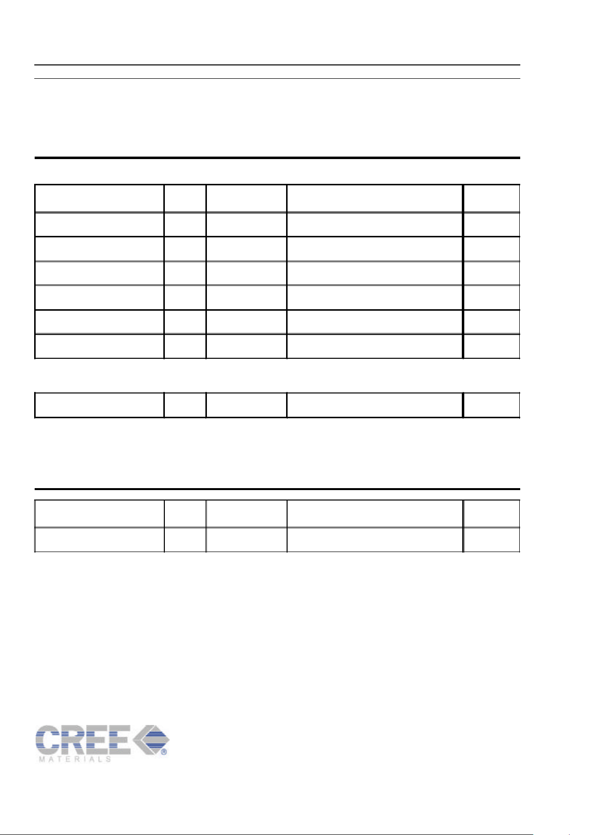
Part Number Type Orientation Resistivity Ohm-cm Range Bin
W6NXD3J-0000 n 3.5° off 0.020-0.040 J
W6NXD3K-0000 n 3.5° off 0.040-0.090 K
W6NXD0K-0000 n on-axis 0.040-0.090 K
W6NXD0KLSR-0000 n on-axis 0.040-0.090 K
W6NXD3L-0000 n 3.5° off 0.090-0.150 L
W6PXD3O-0000 p 3.5° off 1.00-5.00 O
LCW SUBSTRATES
W6NRD0X-0000 n on-axis 0.020-0.200 N/A
Part Number Type Orientation Resistivity Ohm-cm Range Bin
W6NRE0X-0000 n on-axis 0.020-0.200 N/A
Page 7

Effective December 1998 • Revised March 2003 • Page 7
DEFINITION OF DIMENTIONAL PROPERTIES, TERMINOLOGY AND METHODS
Figure 1. Diameter and Primary and Secondary
Flat Dimension
Standard Specifications
Diameter
The linear dimension across the surface of a wafer.
Measurement is performed manually with ANSI
certified digital calipers on each individual wafer (see
Figure 1).
Thickness, Center Point
Measured with ANSI certified non-contact tools at the
center of each individual wafer.
Flat Length
Linear dimension of the flat measured with ANSI
certified digital calipers on a sample of one wafer per
ingot (see Figure 1).
Surface Orientation
Denotes the orientation of the surface of a wafer with
respect to a crystallographic plane within the lattice
structure. Measured with x-ray goniometer on a sample
of one wafer per ingot in the center of the wafer.
Orthogonal Misorientation
In wafers cut intentionally “off orientation,” the angle
between the projection of the normal vector to the
wafers surface onto a {0001} plane and the projection
on that plane of the nearest <1120> direction.
Primary Flat
The primary flat is the {1010} plane with the flat face
parallel to the <1120> direction.
Primary Flat Orientation
The flat of the longest length on the wafer, oriented
such that the chord is parallel with a specified low
index crystal plane. Measured on one wafer per ingot
using Laue back-reflection technique with manual
angle measurement.
Secondary Flat Orientation
A flat of shorter length than the primary orientation
flat, whose position with respect to the primary orientation flat identifies the face of the wafer.
Marking
The carbon face of each individual wafer is laser
marked with OCR compatible font (similar to definitions and characteristics in SEMI M12).
XXXXXXX-XX
Page 8

Page 8 • Effective December 1998 • Revised March 2003
SUBSTRATE PROPERTY CREE STANDARD
Diameter
2.000" ± 0.015"
50.8mm ± 0.38mm
Thickness, Centerpoint
4H and 6H On-Axis
Standard
0.010" ± 0.001"
254.0µm ± 25.4µm
Laser (6H only)
0.0055" ± 0.0015"
140.0µm ± 38.0µm
4H and 6H Off-Axis; Semi-Insulating
0.0145" ± 0.0025"
368.0µm ± 64.0µm
Dopant
n-type: Nitrogen
p-type: Aluminum
Primary Flat Length
0.625" ± 0.065"
15.88mm ± 1.65mm
Secondary Flat Length
0.315" ± 0.065"
8.0mm ± 1.65mm
Cleaved Flat Length (laser substrate only) Nominal 0.4" (10mm)
Surface Orientation
6H and 4H On-Axis {0001} ± 0.5°
6H Off-Axis 3.5° toward <1120> ± 0.5°
4H Off-Axis 8.0° toward <1120> ± 0.5°
Surface Treatment Silicon face polish unless otherwise specified
Orthogonal Misorientation ± 5°
Primary Flat Orientation <1120> ± 5°
Secondary Flat Orientation
Carbon Face 90° CCW from Primary ± 5°
Silicon Face 90° CW from Primary ± 5°
Cleaved Flat Orientation (laser substrate only) 180° from primary flat is {1010} face
Package FLUOROWARE® Single Wafer Container
Standard Specifications
50.8mm Diameter Substrate Specifications
Page 9

Effective December 1998 • Revised March 2003 • Page 9
SUBSTRATE PROPERTY CREE STANDARD
Diameter
3.000" ± 0.015"
76.2mm ± 0.38mm
Thickness, Centerpoint
4H On and Off-Axis
0.0138" ± 0.001"
350.0µm ± 25.4µm
Semi-Insulating
0.0145" ± 0.0025"
368.0µm ± 64.0µm
6H On-Axis
0.010" ± 0.001"
254.0µm ± 25.4µm
Dopant n-type: Nitrogen
Primary Flat Length
0.875" ± 0.125"
22.22mm ± 3.17mm
Secondary Flat Length
0.440" ± 0.060"
11.18mm ± 1.52mm
Surface Orientation
4H and 6H On-Axis {0001} ± 0.5°
4H Off-Axis
4.0° toward <1120> ± 0.5°
8.0° toward <1120> ± 0.5°
Surface Treatment Silicon face polish unless otherwise specified
Orthogonal Misorientation ± 5°
Primary Flat Orientation <1120> ± 5°
Secondary Flat Orientation
Carbon Face 90° CCW from Primary ± 5°
Silicon Face 90° CW from Primary ± 5°
Package FLUOROWARE® Single Wafer Container
Standard Specifications
76.2mm Diameter Substrate Specifications
Page 10

Page 10 • Effective December 1998 • Revised March 2003
STANDARD SPECIFICATIONS FOR POLISHED SILICON CARBIDE
SUBSTRATES - Surface Finish
Standard Specifications
Characteristics Production Grade Research Grade
Edge Chips/Indents by diffuse
lighting
†
None Permitted 2 [ 1.5 mm width & depth
Orange Peel/Pits by diffuse lighting*
G
[ 10% area [ 30% area
Polytype Areas by diffuse lighting*
[ 5% area [ 20% area
Striations by diffuse lighting* 3 allowed [ 3mm each 20 allowed [ 7mm each
Area Contamination (stains) by high
intensity light
None Permitted None Permitted
Cracks by high intensity light None Permitted None Permitted
Hex Plate by high intensity light* Cumulative area <10% Cumulative area <30%
Scratches by high intensity light*
5 scratches to 1x wafer diameter
cumulative length.
8 scratches to 1.5x wafer diameter
cumulative length.
Masking Defects (Mounds)*
Quantitative by 200X Microscopic
Inspection
10 defects in 3 or less of the 9
fields inspected in a cross pattern
10 defects in 5 or less of the 9
fields inspected in a cross pattern
Contamination
Quantitative by 200X Microscopic
Inspection
None in inspected fields None in inspected fields
Cumulative Area Defects*
[ 10% area [ 30% area
Notes:
* Defect limits apply to entire wafer surface except for a 2mm edge exclusion area
G
Pits must be < 2mm in distance from one another to be considered a reject cause
†
Edge chips must be > 0.5mm on R grade material to be considered a reject cause
Page 11

Effective December 1998 • Revised March 2003 • Page 11
Standard Specifications
Orange peel
Visually detectable surface roughening when viewed
under diffuse illumination.
Pits
Individual distinguishable surface anomalies, which
appears as a depression in the wafer surface with a
length-to-width ratio less than 5 to 1, and visible under
high intensity illumination.
Foreign Polytypes (also referred to as “Inclusions” or
“Crystallites”)
Regions of the wafer crystallography which are polycrystalline or of a different polytype material than the
remainder of the wafer, such as 4H mixed in with a 6H
type wafer. Poly regions frequently exhibit color
changes or distinct boundary lines, and are judged in
terms of area percent under diffuse illumination.
Scratches
A scratch is defined as a singular cut or groove into the
frontside wafer surface with a length-to-width ratio of
greater than 5 to 1, and visible under hight intensity
illumination.
Striations
Striations in silicon carbide are defined as linear
crystallographic defects extending down from the
surface of the wafer which may or may not pass
through the entire thickness of the wafer, and generally
follow crystallographic planes over its length.
Total Usable Area
A cumulative subtraction of all noted defect areas from
the frontside wafer quality area within the edge exclusion zone. The remaining percent value indicates the
proportion of the frontside surface to be free of all
noted defects (does not include 2mm edge exclusion).
STANDARD SPECIFICATIONS FOR POLISHED SILICON CARBIDE
SUBSTRATES - Surface Finish
(Area) Contamination
Any foreign matter on the surface in localized areas
which is revealed under high intensity (or diffuse)
illumination as discolored, mottled, or cloudy appearance resulting from smudges, stains or water spots.
Cracks
A fracture or cleavage of the wafer that extends from
the frontside surface of the wafer to the back-side
surface of the wafer. Cracks must exceed 0.010” in
length under high intensity illumination in order to
discriminate fracture lines from allowable crystalline
striations. Fracture lines typically exhibit sharp, thin
lines of propagation, which discriminate them from
material striations.
Edge Chips
Any edge anomalies (including wafer saw exit marks)
in excess of 1.5 mm in either radial depth or width. As
viewed under diffuse illumination, edge chips are
determined as unintentionally missing material from
the edge of the wafer.
Edge Exclusion
The outer 2 mm annulus of the wafer is designated as
wafer handling area and is excluded from surface finish
criteria (such as scratches, pits, haze, contamination,
craters, dimples, grooves, mounds, orange peel and saw
marks).
Hex Plate
Hexagonal shaped platelets on the surface of the wafer
which appear silver in color to the unaided eye, under
diffuse illumination.
Masking Defects (also referred to as “Mound”)
A distinct raised area above the wafer frontside surface
as viewed with diffuse illumination.
Definition of Terminology and Methods
Page 12

Page 12 • Effective December 1998 • Revised March 2003
Epitaxial Specifications for
Silicon Carbide
Notes: • 2mm edge exclusion
• N-type epi layers <20 microns are preceeded by n-type , 1E18, 0.5 micron buffer layer
• N-type epi layers 20 microns are preceeded by n-type , 1E18, 1.0 micron buffer layer
• No buffer layer for p-type epitaxial layers
• Not all doping densities are available in all thicknesses
• Epitaxy on 6H polytype is limited to 10 microns
• Contact Cree Sales for specifications on multi-layer or unique epitaxy requests
STANDARD SPECIFICATIONS FOR SILICON CARBIDE EPITAXIAL WAFER -
50.8mm and 76.2mm SUBSTRATES
Substrate Orientation: Epitaxy is only available for off-axis substrates.
Conductivity n-type p-type
Dopant Nitrogen Aluminum
Net Doping Density ND-N
A
NA-N
D
Silicon Face 9E14 – 1E19/cm
3
9E14 – 1E19/cm
3
Carbon Face 1E16 – 1E19/cm
3
Not Available
Tolerance ± 50% ± 50%
Thickness Range- Silicon Face
0.2-1.0 microns ± 25% of selected thickness ± 25% of selected thickness
1.1-20.0 microns ± 15% of selected thickness ± 15% of selected thickness
20.1-50.0 microns ± 10% of selected thickness ± 10% of selected thickness
Thickness Range- Carbon Face
0.2-1.0 microns ± 25% of selected thickness Not Available
1.0-10.0 microns ± 15% of selected thickness Not Available
á
Page 13

Effective December 1998 • Revised March 2003 • Page 13
Epitaxial Specifications for
Silicon Carbide
Notes: • 2mm edge exclusion
STANDARD SPECIFICATIONS FOR SILICON CARBIDE EPITAXIAL WAFER -
50.8mm and 76.2mm SUBSTRATES
Characteristics
Maximum Acceptability
Limits
Test
Methods
Defect Definitions
(see pgs. 14-15)
Methodology
Large Point Defects
50.8mm 30
Diffuse
Illumination
D1 M1, M2
76.2mm 60
Scratches 10 lines < 2x wafer diameter D2 M1, M2
Dimpling < 5% affected D3 M1, M2
Step Bunching
4° off-axis N/A
D4 M1, M2
8° off-axis < 10% affected
Backside
Cleanliness
95% clean D5 M1, M2
Edge Chips 2 with radius 1.5mm D6 M2
ID Correct/Legible Yes D7 M2
Wafer Flats Yes D7 M2
Epi Defects
50.8mm, 4H 75
Microscopic
D8-D12 M3
50.8mm, 6H 135
76.2mm, 4H 113
76.2mm, 6H 203
Net Doping See Specification Table Hg Probe CV - M4
Thickness See Specification Table
FTIR, SIMS,
SEM
- M5
Page 14

Page 14 • Effective December 1998 • Revised March 2003
Definitions
D1. Large Point Defects
Defects which exhibit a clear shape to the unassisted
eye and are > 50 microns across. These features
include spikes, adherent particles, chips and craters.
Large point defects less than 3 mm apart count as one
defect.
D2. Scratches
Grooves or cuts below the surface plane of the wafer
having a length-to-width ratio of greater than 5 to 1.
Scratches are specified by the number of discrete
scratches times the total length in fractional diameter.
D3. Dimpling
A texture resembling the surface of a golf ball. Specified in % affected area.
D4. Step Bunching
Step bunching is visible as a pattern of parallel lines
running perpendicular to the major flat. If present,
estimate the % of specified area affected.
D5. Backside Cleanliness
Verified by inspecting for a uniform color to the wafer
backside. Note there is a darker region near the center
of some higher doped wafers. Backside cleanliness
specified as percent area clean.
D6. Edge Chips
Areas where material has been unintentionally removed
from the wafer. Do not confuse fractures in epi crown
with edge chips.
D7. ID Correct and Major Wafer Flat
Both should be readily discernible.
Epitaxy Defects
The sum of discrete microscopic defects counted in
specified area. These include 3C inclusions, comet
tails, carrots, particles and silicon droplets.
D8. 3C Inclusions
Regions where step-flow was interrupted during epi
layer growth. Typical regions are generally triangular
although more rounded shapes are sometimes seen.
Count once per occurrence. Two inclusions within 200
microns count as one.
D9. Comet Tails
Comet tails have a discrete head and trailing tail. These
features are aligned parallel to the major flat. Usually,
all comet tails tend to be of the same length. Count
once per occurrence. Two comet tails within 200
microns count as one.
D10. Carrots
Similar to comet tails in appearance except they are
more angular and lack a discrete head. If present, these
features are aligned parallel to the major flat. Usually,
any carrots present tend to be of the same length. Count
once per occurrence. Two carrots within 200 microns
count as one.
D11. Particles
Particles have the appearance of eyes and if present are
usually concentrated at the wafer edges and not within
the specified area. If present, count once per occurrence. Two particles within 200 microns count as one.
D12. Silicon droplets
Silicon droplets can appear as either small mounds or
depressions in the wafer surface. Normally absent, but
if present are largely concentrated at perimeter of
wafer. If present, estimate the % of specified area
affected.
STANDARD SPECIFICATIONS FOR SILICON CARBIDE EPITAXIAL WAFER,
DEFINITIONS, EPITAXY DEFECT DESCRIPTIONS, AND METHODOLOGY
Epitaxial Specifications for
Silicon Carbide
Page 15

Effective December 1998 • Revised March 2003 • Page 15
Methodology
M1. 2mm edge exclusion.
M2. Inspection performed under diffuse illumination.
M3. Microscopic inspection performed at 100X, on an
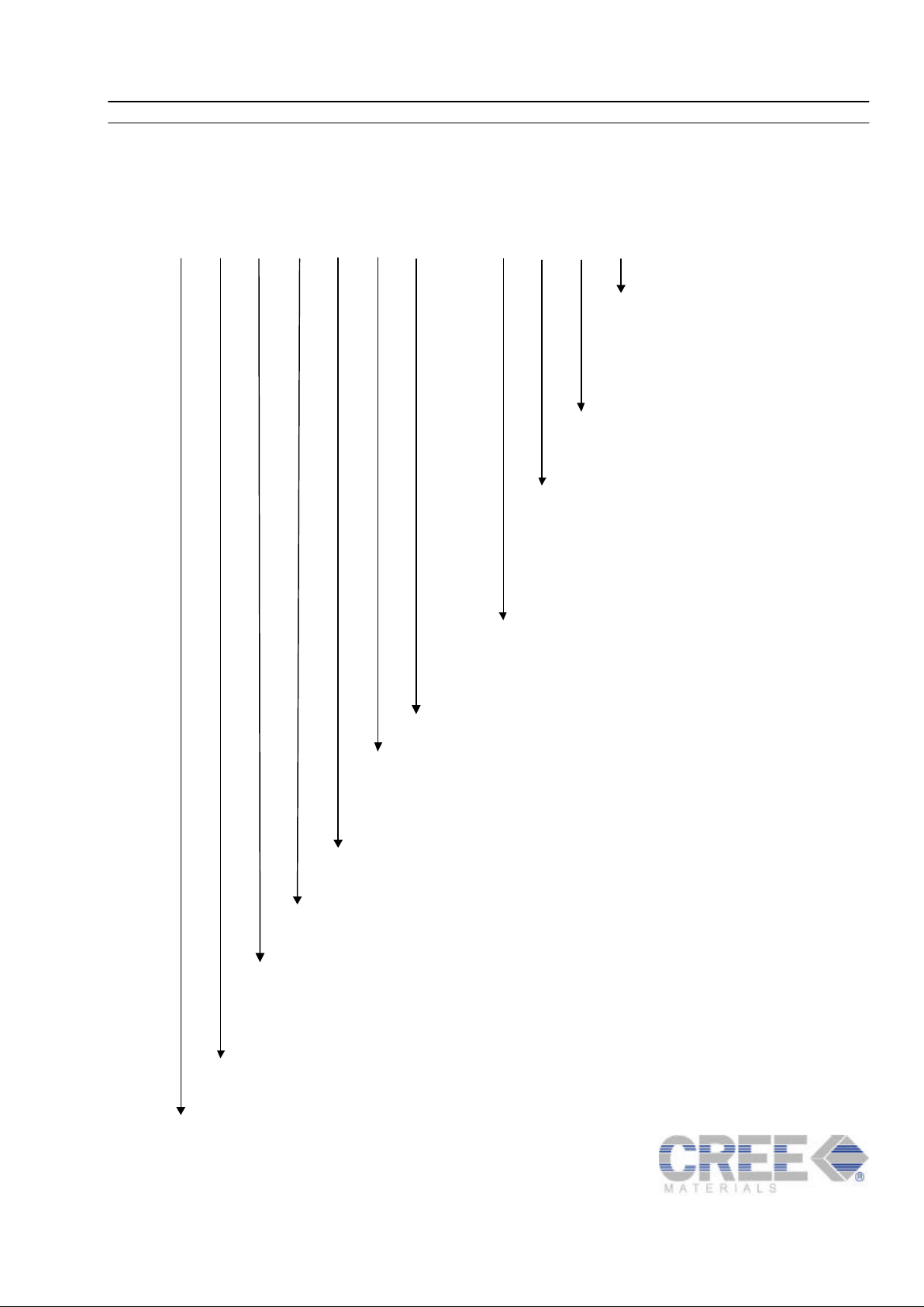
Olympus BH2 UMA Optical Microscope, or comparable. Inspection pattern detailed in Figure 2.
M4. Net doping is determined in the center of the
wafer using Hg probe CV.
M5. Thickness is determined in the center of the wafer
using FTIR, SIMS, or cross-sectional SEM on available
monitor wafers.
Figure 2. Epi Inspection Pattern
STANDARD SPECIFICATIONS FOR SILICON CARBIDE EPITAXIAL WAFER,
DEFINITIONS, EPITAXY DEFECT DESCRIPTIONS, AND METHODOLOGY
Epitaxial Specifications for
Silicon Carbide
Page 16

Page 16 • Effective December 1998 • Revised March 2003
4600 Silicon Drive
Durham, NC 27703 USA
tel: 919-313-5300
fax: 919-313-5451
e-mail: sales@cree.com
www.cree.com
Copyright © 1998-2003 Cree, Inc. All rights reserved.
Permission is given to reproduce this document provided the entire
document (including this copyright notice) is duplicated.
The information in this document is subject to change without notice.
Cree and the Cree logo are registered trademarks of Cree, Inc.
Version MAT-CATALOG.000
Page 17

 Loading...