

Page 1

Preliminary W742C810
4-BIT MICROCONTROLLER
Table of Contents-
1. GENERAL DESCRIPTION..........................................................................................................................3
2. FEATURES..................................................................................................................................................3
3. PIN CONFIGURATION................................................................................................................................4
4. PIN DESCRIPTION......................................................................................................................................5
4.1 Pad List..................................................................................................................................................6
5. BLOCK DIAGRAM.......................................................................................................................................8
6. FUNCTIONAL DESCRIPTION ....................................................................................................................9
6.1 Program Counter (PC)...........................................................................................................................9
6.2 Stack Register (STACK)........................................................................................................................9
6.3 Program Memory (ROM).......................................................................................................................9
6.3.1 ROM Page Register (ROMPR)................................................................................................10
6.4 Data Memory (RAM)............................................................................................................................10
6.4.1 Architecture ..............................................................................................................................10
6.4.2 Page Register (PAGE).............................................................................................................11
6.4.3 WR Page Register (WRP).......................................................................................................12
6.4.4 Data Bank Register (DBKR).....................................................................................................12
6.5 Accumulator (ACC)..............................................................................................................................13
6.6 Arithmetic and Logic Unit (ALU)...........................................................................................................13
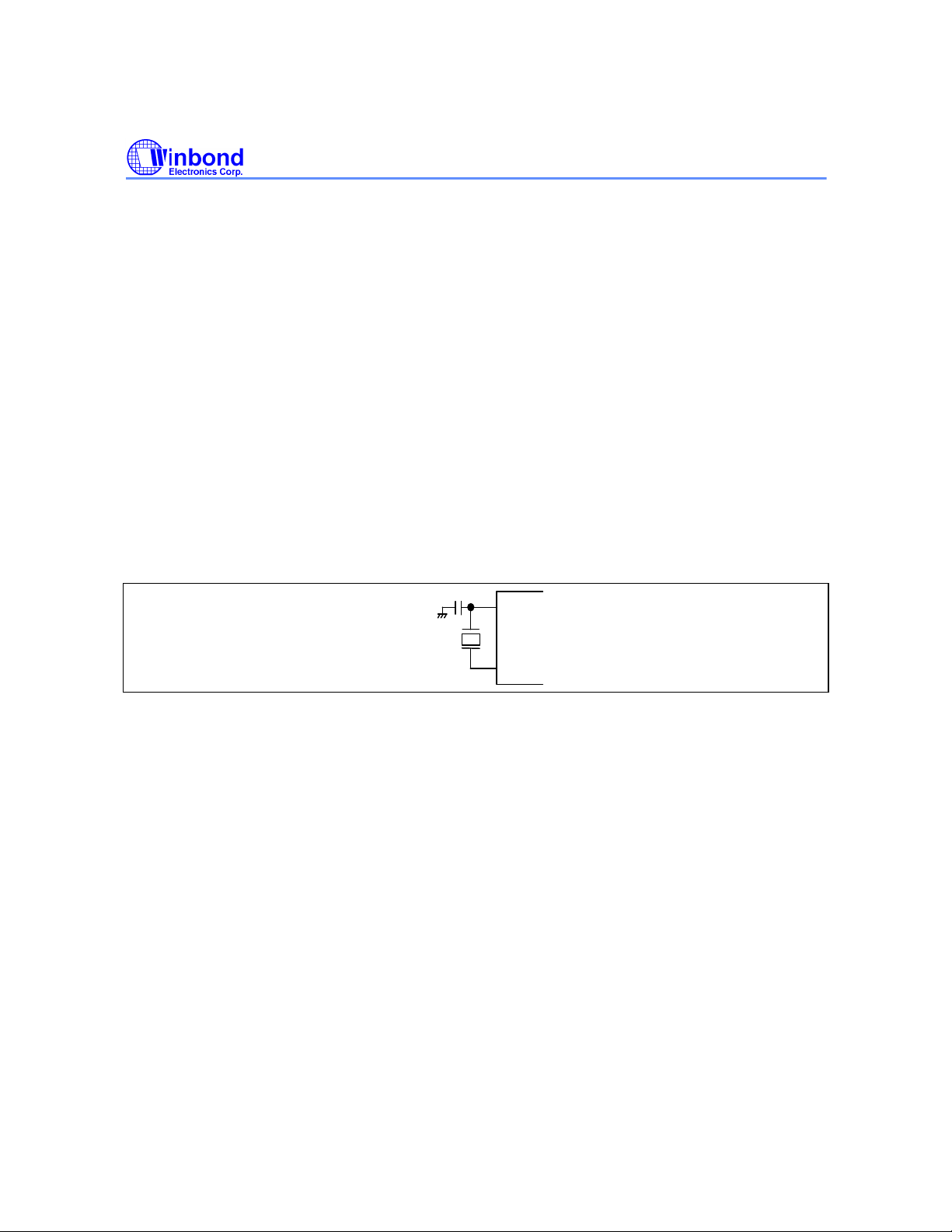
6.7 Main Oscillator......................................................................................................................................13
6.8 Sub-Oscillator.......................................................................................................................................13
6.9 Dividers................................................................................................................................................13
6.10 Dual-clock operation...........................................................................................................................14
6.11 Watchdog Timer (WDT).....................................................................................................................15
6.12 Timer/Counter....................................................................................................................................15
6.12.1 Timer 0 (TM0).........................................................................................................................15
6.12.2 Timer 1 (TM1).........................................................................................................................16
6.12.3 Mode Register 0 (MR0)..........................................................................................................17
6.12.4 Mode Register 1 (MR1)..........................................................................................................17
6.13 Interrupts............................................................................................................................................18
6.14 Stop Mode Operation.........................................................................................................................19
6.14.1 Stop Mode Wake-up Enable Flag for RC Port (SEF).............................................................19
Publication Release Date: May 1999
- 1 - Revision A1
Page 2

Preliminary W742C810
6.15 Hold Mode Operation.........................................................................................................................19
6.15.1 Hold Mode Release Enable Flag (HEF).................................................................................20
6.15.2 Interrupt Enable Flag (IEF) .....................................................................................................21
6.15.3 Port Enable Flag (PEF)..........................................................................................................21
6.15.4 Hold Mode Release Condition Flag (HCF).............................................................................22
6.15.5 Event Flag (EVF)....................................................................................................................22
6.16 Reset Function...................................................................................................................................23
6.17 Input/Output Ports RA, RB & RD .......................................................................................................23
6.17.1 Port Mode 0 Register (PM0)...................................................................................................24
6.17.2 Port Mode 1 Register (PM1)...................................................................................................24
6.17.3 Port Mode 2 Register (PM2)...................................................................................................25
6.17.4 Port Mode 5 Register (PM5)...................................................................................................25
6.18 Input Ports RC....................................................................................................................................25
6.18.1 Port Status Register 0 (PSR0) ...............................................................................................26
6.19 Output Port RE & RF .........................................................................................................................27
6.20 DTMF Output Pin (DTMF)..................................................................................................................27
6.20.1 DTMF register.........................................................................................................................28
6.20.2 Dual Tone Control Register (DTCR).......................................................................................28
6.21 MFP Output Pin (MFP).......................................................................................................................28
6.22 LCD Controller/Driver.........................................................................................................................30
6.22.1 LCD RAM addressing method................................................................................................31
6.22.2 The output waveforms for the LCD driving mode...................................................................31
7. ABSOLUTE MAXIMUM RATINGS............................................................................................................33
8. DC CHARACTERISTICS...........................................................................................................................33
9. AC CHARACTERISTICS...........................................................................................................................34
10. INSTRUCTION SET TABLE....................................................................................................................35
11. PACKAGE DIMENSIONS........................................................................................................................41
- 2 -
Page 3

Preliminary W742C810
1. GENERAL DESCRIPTION
The W742C810 is a high-performance 4-bit microcontroller (µC) that provides an LCD driver. The
device contains a 4-bit ALU, two 8-bit timers, two dividers (for two oscillators) in dual-clock operation,
a 40 × 4 LCD driver, six 4-bit I/O ports (including 1 output port for LED driving), and one channel
DTMF generator. There are also five interrupt sources and 8-level subroutine nesting for interrupt
applications. The W742C810 operates on very low current and has one power reduction mode, that is
the dual-clock slow operation, which helps to minimize power dissipation.
2. FEATURES
• Operating voltage: 2.4V−3.6V
• Dual-clock operation
• Main oscillator
− Connect to 3.58 MHz crystal only
• Sub-oscillator
− Connect to 32768 Hz crystal only
• Memory
− 8192 x 16 bit program ROM (including 32K x 4 bit look-up table)
− 1024 x 4 bit data RAM (including 16 nibbles x 16 pages working registers)
− 40 x 4 LCD data RAM
• 24 input/output pins
− Port for input only: 1 ports/4 pins
− Input/output ports: 3 ports/12 pins
− High sink current output port for LED driving: 1 port /4 pins
− Port for output only: 1 port/ 4 pins
• Power-down mode
− Hold function: no operation (main oscillator and sub-oscillator still operate)
− Stop function: no operation (only main oscillator stops but sub-oscillator still operates)
− Dual-clock slow mode: system is operated by the sub-oscillator (FOSC = Fs and Fm is stopped)
• Five types of interrupts
− Four internal interrupts (Divider0, Divider1, Timer 0, Timer 1)
− One external interrupt (RC Port)
• LCD driver output
− 40 segments x 4 commons
− 1/4 duty 1/3 bias driving mode
− Clock source should be the sub-oscillator clock in the dual-clock operation mode
• MFP output pin
− Output is software selectable as modulating or nonmodulating frequency
− Works as frequency output specified by Timer 1
Publication Release Date: May 1999
- 3 - Revision A1
Page 4
Preliminary W742C810
CNCNCNC
CNCNCNC
• DTMF output pin
− Output is one channel Dual Tone Multi-frequency signal for dialling
• Two built-in 14-bit frequency dividers
− Divider0: the clock source is the output of the main oscillator
− Divider1: the clock source is the output of the sub-oscillator
• Two built-in 8-bit programmable countdown timers
− Timer 0: one of two internal clock frequencies (FOSC/4 or FOSC/1024) can be selected
− Timer 1: with auto-reload function, and one of three internal clock frequencies (FOSC, FOSC/64 or
Fs) can be selected by MR1 register; the specified frequency can be delivered to MFP pin
• Built-in 18/15-bit watchdog timer selectable for system reset; enable the watch dog timer or not is
determined by code option
• Powerful instruction set: 131 instructions
• 8-level subroutine (include interrupt) nesting
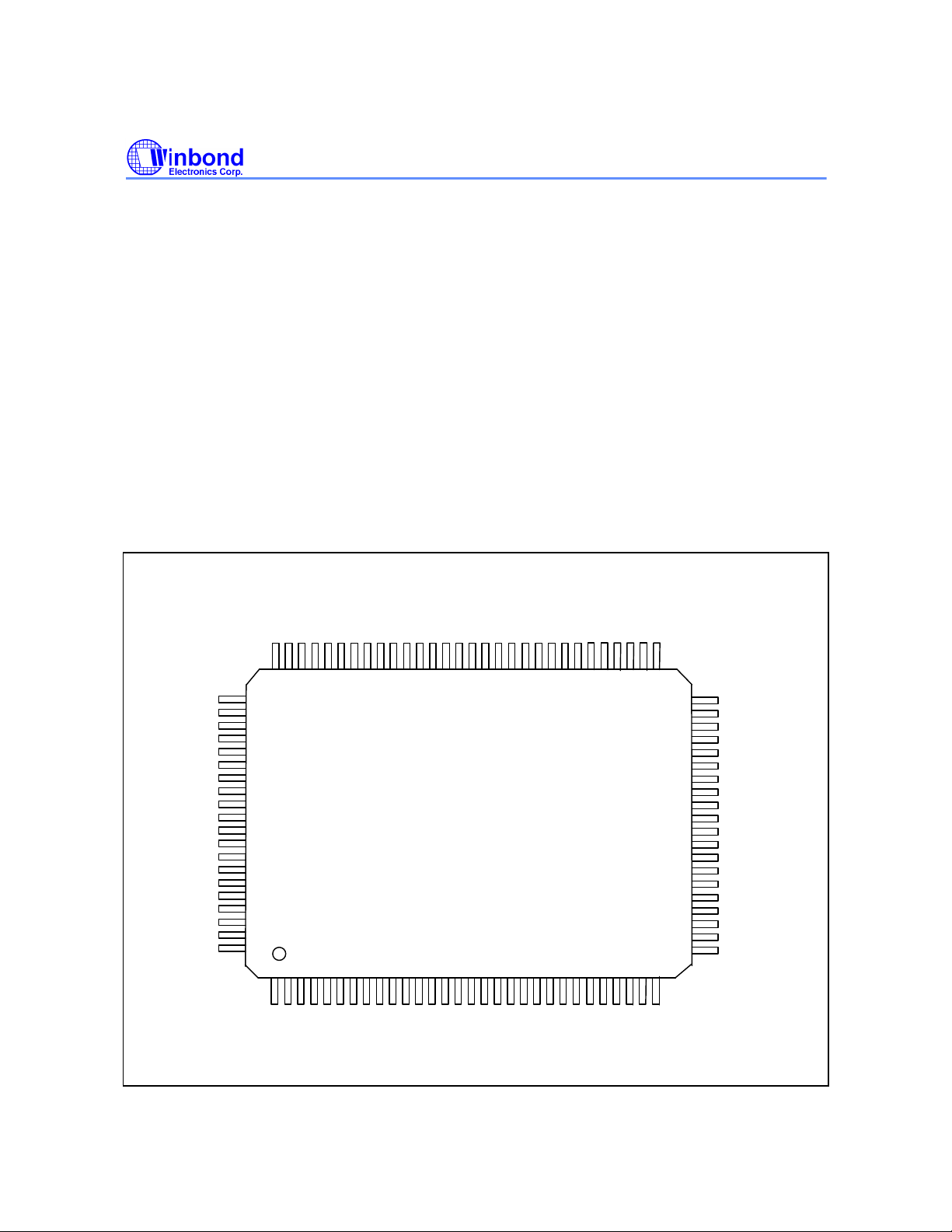
3. PIN CONFIGURATION
NC
MFP
RA0
RA1
RA2
RA3
RB0
RB1
RB2
RB3
RC0
RC1
RC2
RC3
RD0
RD1
RD2
RD3
RE0
NC
X
X
O
X
O
X
D
I
T
R
N
M
E
N
1
F
S
80 79 78 77 76 75 74 73 72 717069 68 67 666564 63 62
81
82
83
84
85
86
87
88
89
90
91
92
93
94
95
96
97
98
99
100
1 2 3
4 5 6 7 8 91011 12 13 14 15 16 17 18 19
R
N
C
NCNCN
R
R
E
E
C
E
1
2
3
U
I
V
U
T
N
D
T
2
2
D
1
R
R
R
R
F
F
F
F
0
1
2
3
V
V
D
D
D
D
D
D
H
H
2
1
2
1
V
S
S
S
S
E
E
E
S
G
G
G
0
1
2
C
O
O
O
M
M
M
2
1
0
S
S
S
E
E
E
G
G
G
3
4
5
G
G
O
3
3
M
8
9
3
61 60 59 58 57
20 21 22 23 24
S
S
S
E
E
E
G
G
G
6
7
8
G
3
7
S
E
G
9
S
E
E
E
C
C
C
E
E
G
G
3
3
5
6
56 55 54 53 52
S
S
E
E
G
G
1
1
0
1
E
E
G
G
3
3
3
4
25 26 27 28
S
S
NCNCN
E
E
G
G
1
1
2
3
N
51
30
29
N
C
C
50
49
48
47
46
45
44
43
42
41
40
39
38
37
36
35 SEG18
34
33
32
31
NC
SEG32
SEG31
SEG30
SEG29
SEG28
SEG27
SEG26
SEG25
SEG24
SEG23
SEG22
SEG21
SEG20
SEG19
SEG17
SEG16
SEG15
SEG14
S
S
S
S
S
S
- 4 -
Page 5
Preliminary W742C810
RES
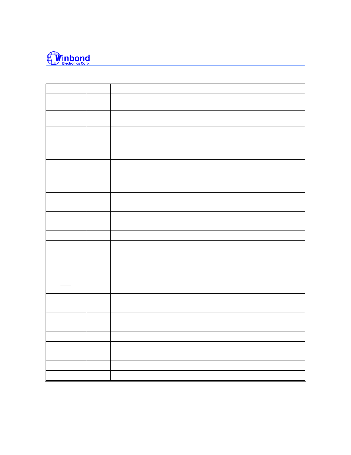
4. PIN DESCRIPTION
SYMBOL I/O FUNCTION
XIN2 I Input pin for sub-oscillator.
Connected to 32.768 Khz crystal only.
XOUT2 O Output pin for sub-oscillator with internal oscillation capacitor. Connected
to 32.768 Khz crystal only.
XIN1 I Input pin for main-oscillator.
Connected to 3.58MHz crystal to generate system clock.
XOUT1 O Output pin for main-oscillator.
Connected to 3.58MHz crystal to generate system clock.
RA0-RA3 I/O Input/Output port.
Input/output mode specified by port mode 1 register (PM1).
RB0-RB3 I/O Input/Output port.
Input/output mode specified by port mode 2 register (PM2).
RC0-RC3 I 4-bit port for input only.
Each pin has an independent interrupt capability.
RD0-RD3 I/O Input/Output port
Input/Output mode specified by port mode 5 register (PM5)
RE0-RE3 O Output port only. With high sink current capacity for the LED application.
RF0-RF3 O Output port only.
Output pin only.
MFP O
DTMF O This pin can output dual-tone multifrequency signal for dialling.
SEG0-
SEG39
COM0-
COM3
DH1, DH2 I Connection terminals for voltage doubler (halver) capacitor.
VDD1
VDD2 I
VDD I Positive power supply (+).
VSS I Negative power supply (-).
O LCD segment output pins.
O LCD common signal output pins.
This pin can output modulating or nonmodulating frequency, or Timer 1
clock output specified by mode register 1 (MR1).
I System reset pin with pull-high resistor.
Positive (+) supply voltage terminal.
Refer to Functional Description.
Publication Release Date: May 1999
- 5 - Revision A1
Page 6

Preliminary W742C810
4.1 Pad List
** Shrink factor: 1.000000; Date: 1997/12/31; Time: 14:46:10
** Window: (xl = -1410.00, yl = -1595.00), (xh = 1410.00, yh = 1595.00)
** Windows size: width = 2820.00, length = 3190.00
PAD NO. PAD NAME PIN NAME X Y
1 RE1 5 -1302.45 1336.70
2 RE2 6 -1302.45 1205.53
3 RE3 7 -1302.45 1075.53
4 RF0 8 -1302.45 944.00
5 RF1 9 -1302.45 817.58
6 RF2 10 -1302.45 693.58
7 RF3 11 -1302.45 569.58
8 VSS 12 -1302.45 407.95
9 SEG<0> 13 -1302.45 283.95
10 SEG<1> 14 -1302.45 159.95
11 SEG<2> 15 -1302.45 35.95
12 SEG<3> 16 -1302.45 -88.05
13 SEG<4> 17 -1302.45 -212.05
14 SEG<5> 18 -1302.45 -336.05
15 SEG<6> 19 -1302.45 -460.05
16 SEG<7> 20 -1302.45 -584.05
17 SEG<8> 21 -1302.45 -708.05
18 SEG<9> 22 -1302.45 -832.05
19 SEG<10> 23 -1302.45 -956.38
20 SEG<11> 24 -1302.45 -1086.40
21 SEG<12> 25 -1302.45 -1216.40
22 SEG<13> 26 -1302.45 -1350.40
23 SEG<14> 31 -1302.45 -1486.30
24 SEG<15> 32 -1025.28 -1489.60
25 SEG<16> 33 -895.28 -1489.60
26 SEG<17> 34 -765.28 -1489.60
27 SEG<18> 35 -635.28 -1489.60
28 SEG<19> 36 -505.28 -1489.60
29 SEG<20> 37 -375.28 -1489.60
30 SEG<21> 38 -251.28 -1489.60
- 6 -
Page 7
Preliminary W742C810
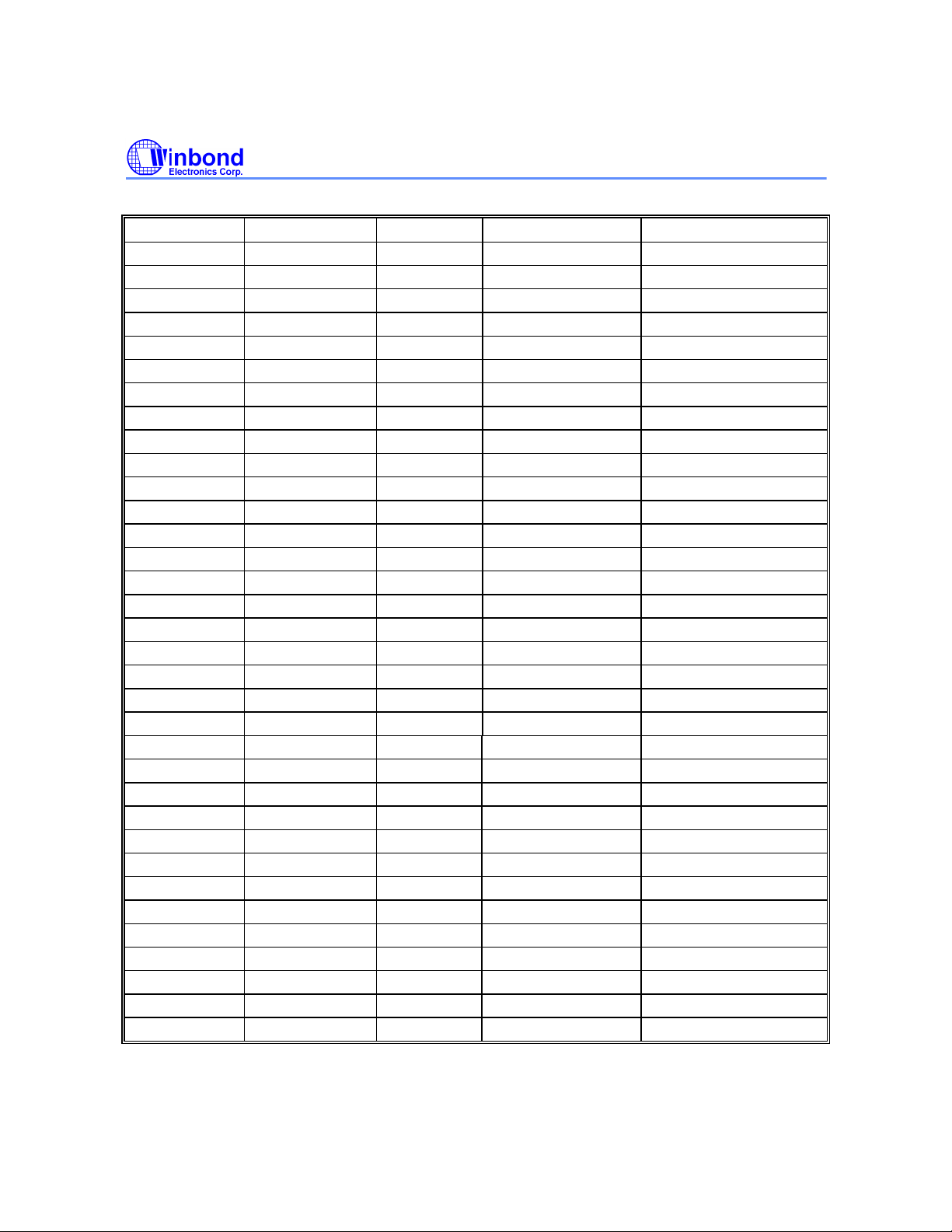
Pad List, continued
PAD NO. PAD NAME PIN NAME X Y
31 SEG<22> 39 -127.28 -1489.60
32 SEG<23> 40 -3.28 -1489.60
33 SEG<24> 41 120.73 -1489.60
34 SEG<25> 42 244.73 -1489.60
35 SEG<26> 43 368.73 -1489.60
36 SEG<27> 44 498.73 -1489.60
37 SEG<28> 45 628.73 -1489.60
38 SEG<29> 46 758.73 -1489.60
39 SEG<30> 47 888.73 -1489.60
40 SEG<31> 48 1018.73 -1489.60
41 SEG<32> 49 1301.23 -1486.30
42 SEG<33> 55 1301.23 -1356.30
43 SEG<34> 56 1301.23 -1222.30
44 SEG<35> 57 1301.23 -1100.30
45 SEG<36> 58 1301.23 -970.30
46 SEG<37> 59 1301.23 -840.30
47 SEG<38> 60 1301.23 -716.30
48 SEG<39> 61 1301.23 -592.30
50 COM<2> 63 1301.23 -319.90
51 COM<1> 64 1301.23 -179.10
52 COM<0> 65 1301.23 -38.30
53 VDD2 66 1301.23 118.90
54 VDD1 67 1301.23 263.55
55 DH2 6 1301.23 411.73
56 DH1 69 1301.23 535.73
57 XOUT2 70 1301.23 659.73
58 XIN2 71 1301.23 783.73
59 VDD 72 1301.23 907.73
60 XOUT1 73 1301.23 1075.50
61 XIN1 74 1301.23 1205.50
62 DTMF 75 1301.23 1336.68
63 RES 76 1301.23 1466.70
64 MFP 82 1024.38 1470.00
65 RA0 83 894.38 1470.00
Publication Release Date: May 1999
- 7 - Revision A1
Page 8
Preliminary W742C810
Pad List, ontinued
PAD NO. PAD NAME PIN NAME X Y
66 RA1 84 764.38 1470.00
67 RA2 85 634.38 1470.00
68 RA3 86 504.38 1470.00
69 RB0 87 374.38 1470.00
70 RB1 88 250.38 1470.00
71 RB2 89 126.38 1470.00
72 RB3 90 2.38 1470.00
73 RC0 91 -121.63 1470.00
74 RC1 92 -245.63 1470.00
75 RC2 93 -369.63 1470.00
76 RC3 94 -499.63 1470.00
77 RD0 95 -629.63 1470.00
78 RD1 96 -759.63 1470.00
79 RD2 97 -889.63 1470.00
80 RD3 98 -1019.63 1470.00
81 RE0 99 -1302.45 1466.70
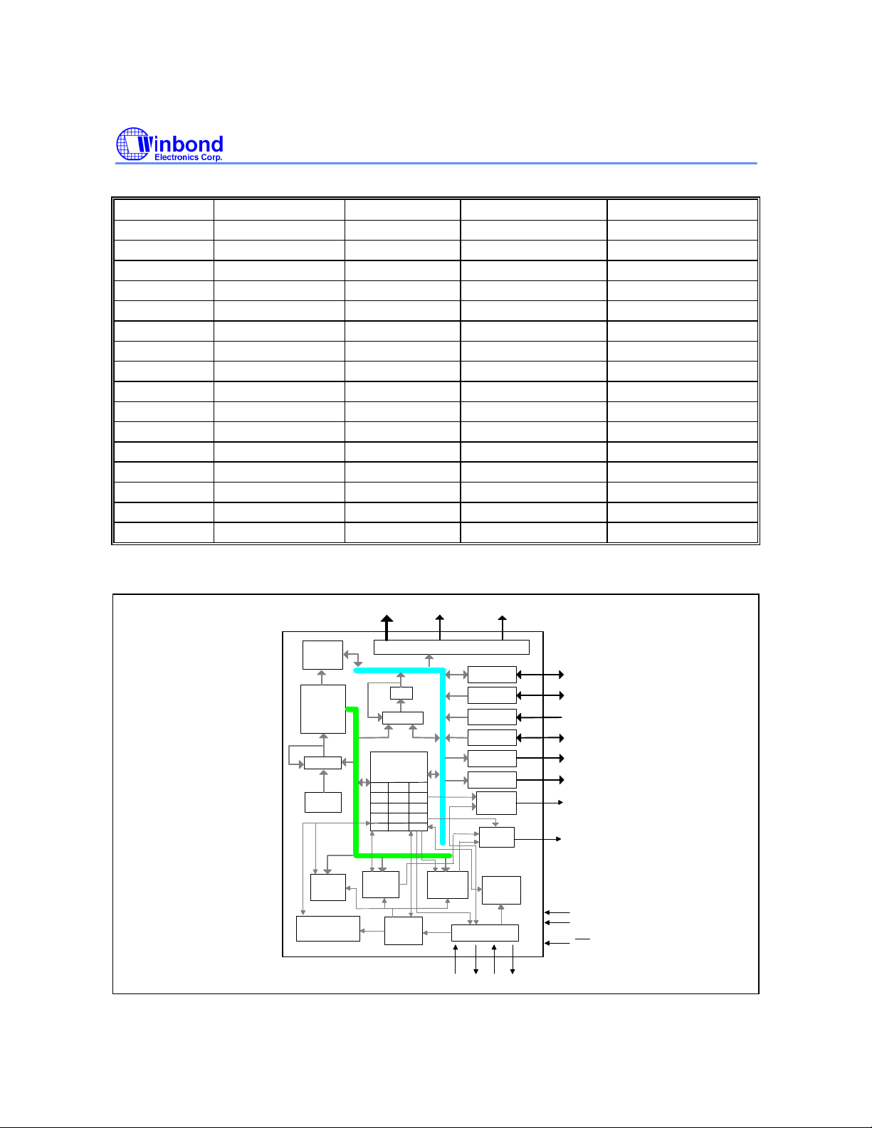
5. BLOCK DIAGRAM
RAM
(1024*4)
ROM
(8192*16)
(look_up table
32K*4)
+1(+2)
PC
STACK
(8 Levels)
Timer 0
(8 Bit)
Watch Dog Timer
(4 Bit)
SEG0~SEG39 COM0~COM4
LCD DRIVER
ACC
ALU
Central Control
Unit
PEFHEFIEF
HCF
EVF SEF
PSR0 SCR PR
MR0 MR1
PM0
. . .
Divider 0
(14 Bit)
Modulation
Frequency
Pulse
XIN2 XOUT2
Timer 1
(8 Bit)
VDD1~VDD2,DH1~2
PORT RA
PORT RB
PORT RC
PORT RD
PORT RE
PORT RF RF0-3
DTMF
Generator
SEL
MUL
Divider 1
(12/14 Bit)
Timing Generator
XIN1
XOUT1
RA0-3
RB0-3
RC0-3
RD0-3
RE0-3
DTMF
MFP
VDD
VSS
RES
- 8 -
Page 9
Preliminary W742C810
6. FUNCTIONAL DESCRIPTION
6.1 Program Counter (PC)
Organized as a 13-bit binary counter (PC0 to PC12), the program counter generates the addresses of
the 8192 × 16 on-chip ROM containing the program instruction words. Before the jump or subroutine
call instructions are to be executed, the destination ROM page must be determined first. The
confirmation of the ROM page can be done by executing the MOV ROMPR, #I or MOV ROMPR, R
instruction. When the interrupt or initial reset conditions are to be executed, the corresponding
address will be loaded into the program counter directly. The format used is shown below.
Table 1 Vector address and interrupt priority
ITEM ADDRESS INTERRUPT PRIORITY
Initial Reset 0000H INT 0 (Divider0) 0004H 1st
INT 1 (Timer 0) 0008H 2nd
INT 2 (Port RC) 000CH 3rd
INT 3 (Divider1) 0014H 4th
INT 4 (Timer 1) 0020H 5th
JP Instruction XXXXH Subroutine Call XXXXH -
6.2 Stack Register (STACK)
The stack register is organized as 13 bits x 8 levels (first-in, last-out). When either a call subroutine or
an interrupt is executed, the program counter will be pushed onto the stack register automatically. At
the end of a call subroutine or an interrupt service subroutine, the RTN instruction must be executed
to pop the contents of the stack register into the program counter. When the stack register is pushed
over the eighth level, the contents of the first level will be lost. In other words, the stack register is
always eight levels deep.
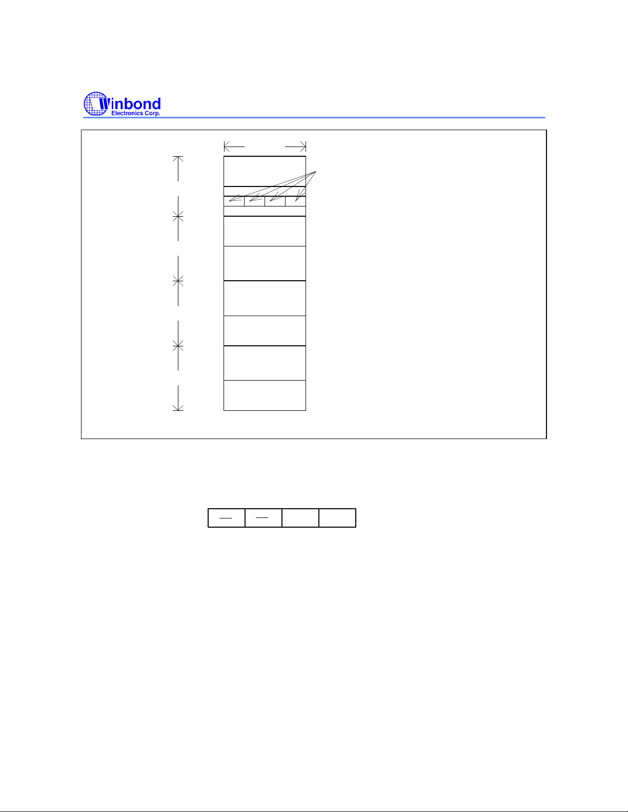
6.3 Program Memory (ROM)
The read-only memory (ROM) is used to store program codes; the look-up table is arranged as 32768
×4 bits. The program ROM is divided into four pages; the size of each page is 2048 × 16 bits. Total
ROM size is therefore 8192 × 16 bits. Before the jump or subroutine call instructions are to be
executed, the destination ROM page must be determined first. The ROM page can be selected by
executing the MOV ROMPR, #I or MOV ROMPR, R instruction. However, the branch decision
instructions (e.g. JB0, SKB0, JZ, JC, ...) must jump to the same ROM page which the branch decision
instructions are located in. The whole ROM range can store both instruction codes and the look-up
table. Each look-up table element is composed of 4 bits, so the look-up table can be addressed up to
32768 elements. Instruction MOVC R is used to read the look-up table content and transfer table data
to the RAM. But before reading the addressed look-up table content, the content of the look-up table
pointer (TAB) must be determined first. The address of the look-up table element is allocated by the
content of TAB. The MOV TAB0 (TAB1, TAB2, TAB3), R instructions are used to allocate the address
of the wanted look-up table element. The TAB0 register stores the LSB 4 bits of the look-up table
address. The organization of the program memory is shown in Figure 6-1.
Publication Release Date: May 1999
- 9 - Revision A1
Page 10
:
:
:
:
:
:
1st page
:
:
:
:
2nd page
3rd page
4th page
0000H
03FFH
0400H
07FFH
0800H
0BFFH
0C00H
0FFFH
1000H
13FFH
1400H
17FFH
1800H
1BFFH
1C00H
1FFFH
16 bits
Look-up Table address:
0000H
:
0FFFH
Look-up Table address:
2000H
:
2FFFH
Look-up Table address:
3000H
:
3FFFH
Look-up Table address:
4000H
:
4FFFH
Look-up Table address:
5000H
:
5FFFH
Look-up Table address:
6000H
:
6FFFH
Look-up Table address:
7000H
:
7FFFH
8192 * 16 bits
Preliminary W742C810
Each element (4 bits) of the look-up table
Look-up Table address:
1000H
:
1FFFH
Figure 6-1 Program Memory Organization
6.3.1 ROM Page Register (ROMPR)
The ROM page register is organized as a 4-bit binary register. The bit descriptions are as follows:
0123
ROMPR
Note: R/W means read/write available.
R/W
R/W
Bit 3 & Bit 2 is reserved.
Bit 1, Bit 0 ROM page preselect bits:
00 = ROM page 0 (0000H - 07FFH)
01 = ROM page 1 (0800H - 0FFFH)
10 = ROM page 2 (1000H - 17FFH)
11 = ROM page 3 (1800H - 1FFFH)
6.4 Data Memory (RAM)
6.4.1 Architecture
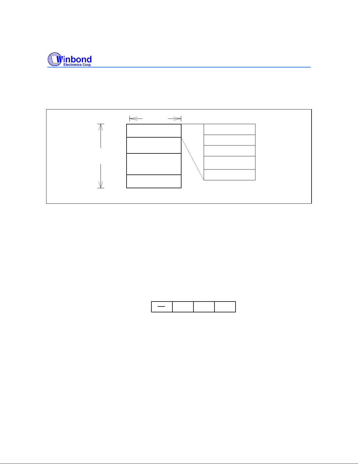
The static data memory (RAM) used to store data is arranged as 1024 × 4 bits. The data RAM is
divided into eight banks; each bank has 128 × 4 bits. Executing the MOV DBKR,WR or MOV
DBKR,#I instruction can determine which data bank is used. The data memory can be addressed
- 10 -
Page 11
Preliminary W742C810
:
:
:
(or Working Registers bank)
(or Working Registers bank)
directly or indirectly. However, the data bank must be confirmed first; the page in the data bank will
be done in the indirect addressing mode, too. In indirect addressing mode, each data bank will be
divided into eight pages. Before the data memory is addressed indirectly, the page which the data
memory is located in must be confirmed. The organization of the data memory is shown in Figure 6-
2.
4 bits
1st data bank
2nd data bank
:
:
:
8th data bank
1024 * 4 bits
Figure 6-2 Data Memory Organization
1st data RAM page
(or 1st WR page)
2nd data RAM page
(or 2nd WR page)
3rd data RAM page
(or 3rd WR page)
:
:
8th data RAM page
(or 8th WR page)
00H
0FH
10H
1FH
20H
2FH
70H
7FH
:
:
:
:
1024
address
000H
07FH
080H
0FFH
380H
3FFH
The 1st and 2nd data bank (00H to 7FH & 80H to FFH) in the data memory can also be used as the
working registers (WR). This is also divided into sixteen pages. Each page contains 16 working
registers. When one page is used as WR, the others can be used as the normal data memory. The
WR page can be switched by executing the MOV WRP,R or MOV WRP,#I instruction. The data
memory cannot operate directly with immediate data, but the WR can do so. The relationship
between data memory locations and the page register (PAGE) in indirect addressing mode is
described in the next sub-section.
6.4.2 Page Register (PAGE)
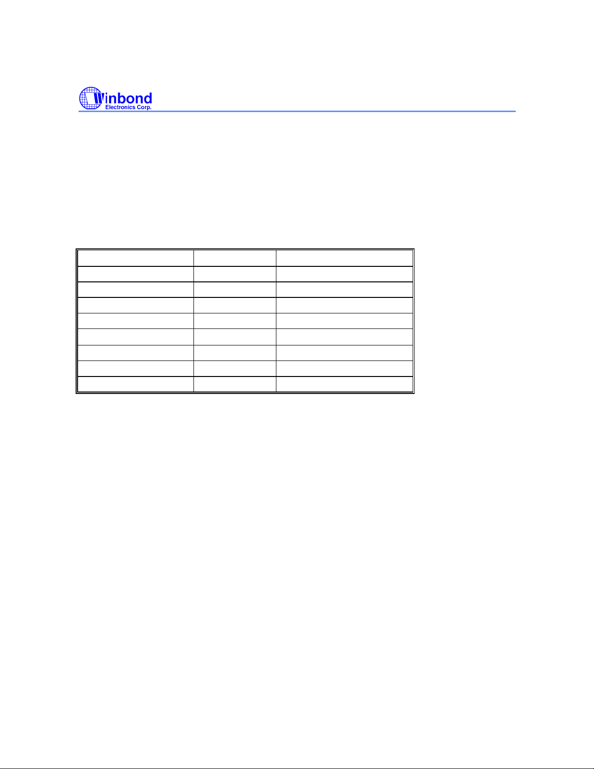
The page register is organized as a 4-bit binary register. The bit descriptions are as follows:
Note: R/W means read/write available.
Bit 3 is reserved.
Bit 2, Bit 1, Bit 0 Indirect addressing mode preselect bits in one data bank:
PAGE
000 = Page 0 (00H - 0FH)
001 = Page 1 (10H - 1FH)
010 = Page 2 (20H - 2FH)
011 = Page 3 (30H - 3FH)
100 = Page 4 (40H - 4FH)
101 = Page 5 (50H - 5FH)
110 = Page 6 (60H - 6FH)
111 = Page 7 (70H - 7FH)
0123
R/W R/W R/W
Publication Release Date: May 1999
- 11 - Revision A1
Page 12
Preliminary W742C810
6.4.3 WR Page Register (WRP)
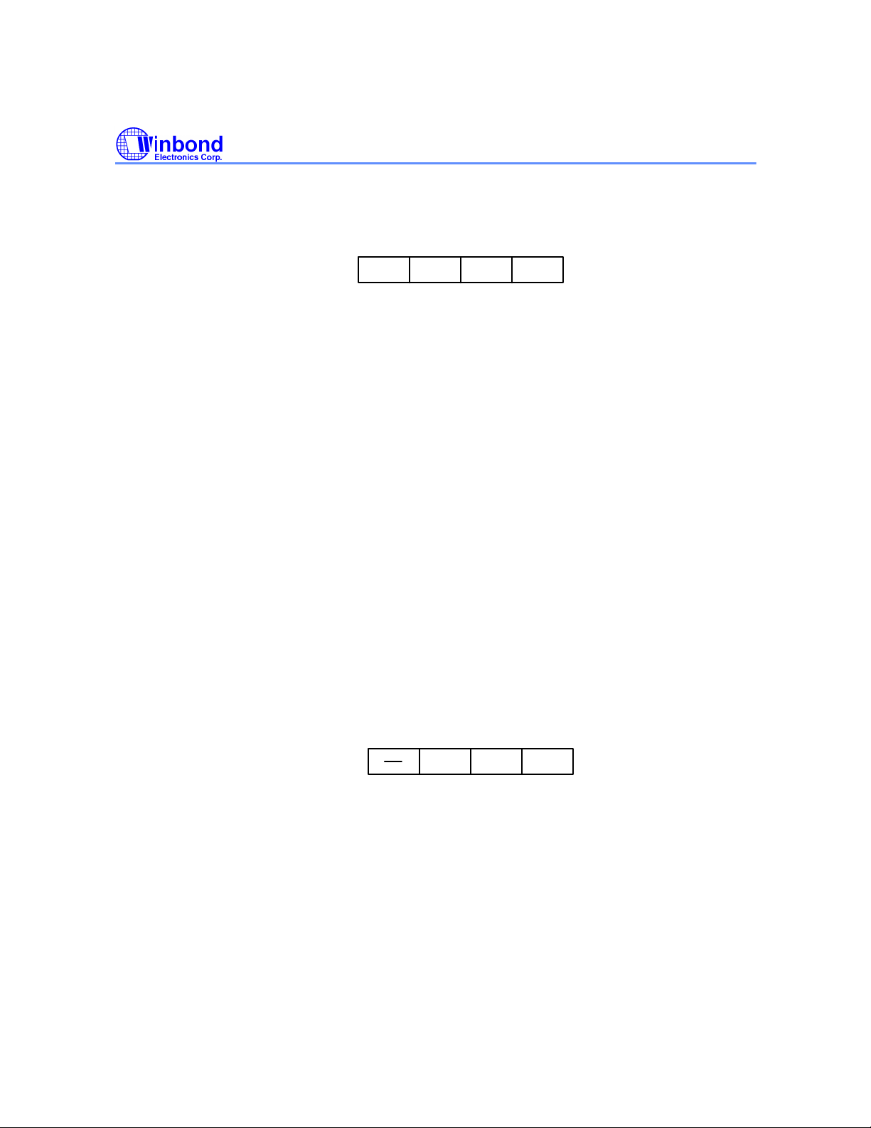
The WR page register is organized as a 4-bit binary register. The bit descriptions are as follows:
0123
WRP
Note: R/W means read/write available.
Bit 3, Bit 2, Bit 1, Bit 0 Working registers page preselect bits:
0000 = WR Page 0 (00H - 0FH)
0001 = WR Page 1 (10H - 1FH)
0010 = WR Page 2 (20H - 2FH)
0011 = WR Page 3 (30H - 3FH)
0100 = WR Page 4 (40H - 4FH)
0101 = WR Page 5 (50H - 5FH)
0110 = WR Page 6 (60H - 6FH)
0111 = WR Page 7 (70H - 7FH)
1000 = WR Page 8 (80H - 8FH)
1001 = WR Page 9 (90H - 9FH)
1010 = WR Page A (A0H - AFH)
1011 = WR Page B (B0H - BFH)
1100 = WR Page C (C0H - CFH)
1101 = WR Page D (D0H - DFH)
1110 = WR Page E (E0H - EFH)
1111 = WR Page F (F0H - FFH)
R/WR/W R/W R/W
6.4.4 Data Bank Register (DBKR)
The data bank register is organized as a 4-bit binary register. The bit descriptions are as follows:
0123
DBKR
Note: R/W means read/write available.
Bit 3 is reserved.
Bit 2, Bit 1, Bit 0 Data memory bank preselect bits:
000 = Data bank 0 (000H - 07FH)
001 = Data bank 1 (080H - 0FFH)
010 = Data bank 2 (100H - 17FH)
011 = Data bank 3 (180H - 1FFH)
100 = Data bank 4 (200H - 27FH)
101 = Data bank 5 (280H - 2FFH)
110 = Data bank 6 (300H - 37FH)
111 = Data bank 7 (380H - 3FFH)
R/W R/W R/W
- 12 -
Page 13
Preliminary W742C810
6.5 Accumulator (ACC)
The accumulator (ACC) is a 4-bit register used to hold results from the ALU and transfer data
between the memory, I/O ports, and registers.
6.6 Arithmetic and Logic Unit (ALU)
This is a circuit which performs arithmetic and logic operations. The ALU provides the following
functions:
• Logic operations: ANL, XRL, ORL
• Branch decisions: JB0, JB1, JB2, JB3, JNZ, JZ, JC, JNC, DSKZ, DSKNZ, SKB0, SKB1, SKB2,
SKB3
• Shift operations: SHRC, RRC, SHLC, RLC
• Binary additions/subtractions: ADC, SBC, ADD, SUB, ADU, DEC, INC
After any of the above instructions are executed, the status of the carry flag (CF) and zero flag (ZF) is
stored in the internal registers. CF can be read out by executing MOV R, CF.
6.7 Main Oscillator
The W742C810 provides a crystal oscillation circuit to generate the system clock through external
connections. The 3.58 MHz crystal must be connected to XIN1 and XOUT1, and a capacitor must be
connected to XIN1 and VSS if an accurate frequency is needed.
XIN1
Crystal
3.58MHz
Figure 6-3 System clock oscillator Configuration
XOUT1
6.8 Sub-Oscillator
The sub-oscillator is used in dual-clock operation mode. In the sub-oscillator application, only the
32768 Hz crystal can be connected to XIN2 and XOUT2, and a capacitor must be connected to XIN2
and VSS if an accurate frequency is needed. The sub-oscillator will be oscillatory continuously in
STOP mode.
6.9 Dividers
Each divider is organized as a 14-bit binary up-counter designed to generate periodic interrupts.
When the main oscillator starts action, the Divider0 is incremented by each clock (FOSC). When an
overflow occurs, the Divider0 event flag is set to 1 (EVF.0 = 1). Then, if the Divider0 interrupt enable
flag has been set (IEF.0 = 1), the interrupt is executed, while if the hold release enable flag has been
set (HEF.0 = 1), the hold state is terminated. The last 4-stage of the Divider0 can be reset by
executing CLR DIVR0 instruction. If the main oscillator is connected to the 32768 Hz crystal, the
EVF.0 will be set to 1 periodically at the period of 500 mS.
If the sub-oscillator starts action, the Divider1 is incremented by each clock (Fs). When an overflow
occurs, the Divider1 event flag is set to 1 (EVF.4 = 1). Then, if the Divider1 interrupt enable flag has
been set (IEF.4 = 1), the interrupt is executed, while if the hold release enable flag has been set
(HEF.4 = 1), the hold state is terminated. The last 4-stage of the Divider1 can be reset by executing
CLR DIVR1 instruction. The same as with EVF.0, the EVF.4 is set to 1 periodically. However, there
Publication Release Date: May 1999
- 13 - Revision A1
Page 14
Preliminary W742C810
are two period times (125 mS & 500 mS) that can be selected by setting the SCR.3 bit. When SCR.3
= 0 (default), the 500 mS period time is selected; SCR.3 = 1, the 125 mS period time is selected.
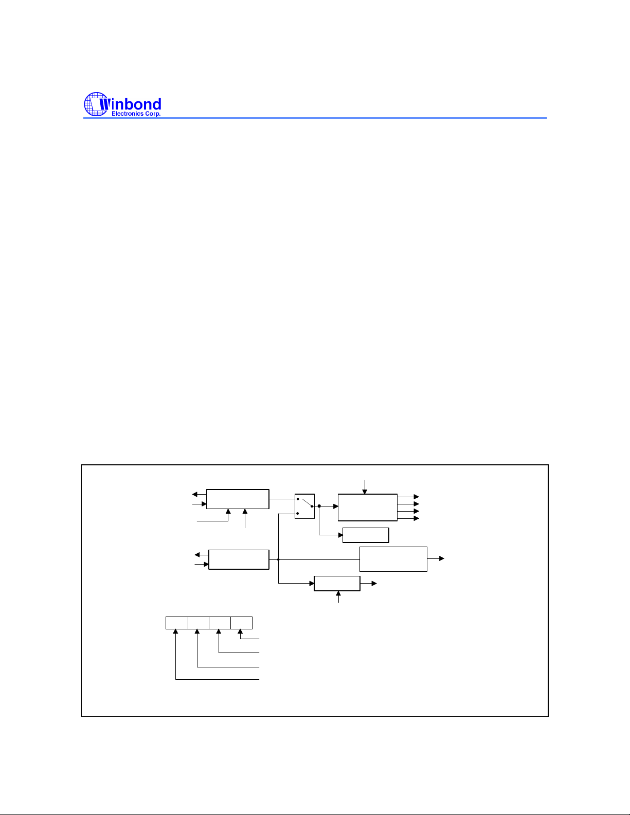
6.10 Dual-clock operation
In the dual-clock mode, the clock source of the LCD frequency selector should be the sub-oscillator
clock (32768 Hz) only. So when the STOP instruction is executing, the LCD will keep working in the
dual-clock mode.
In this dual-clock mode, the normal operation is performed by generating the system clock from the
main-oscillator clock (Fm). The slow operation can be performed as required by generating the
system clock from the sub-oscillator clock (Fs). The exchange of the normal operation and the slow
operation is performed by resetting or setting the bit 0 of the System clock Control Register (SCR). If
the SCR.0 is reset to 0, the clock source of the system clock generator is main-oscillator clock; if the
SCR.0 is set to 1, the clock source of the system clock generator is sub-oscillator clock. In the dualclock mode, the main-oscillator can stop oscillating when the STOP instruction is executing or the
SCR.1 is set to 1.
When the SCR is set or reset, we must be careful in the following cases:
1. X000B → X011B: we should not exchange the FOSC from Fm into Fs and disable Fm
simultaneously. We can first exchange the FOSC from Fm into Fs, then disable the main-oscillator.
So the order should be X000B→X001B→X011B.
2. X011B → X000B: we should not enable Fm and exchange the FOSC from Fs into Fm
simultaneously. We can first enable the main-oscillator; the 2nd step is calling a delay subroutine
to wait until the main-oscillator is oscillating stably; then the last step is to exchange the FOSC from
Fs into Fm. So the order should be X011B→X001B→delay the Fm oscillating stably time→X000B.
We must remember that the X010B state is inhibitive, because it will induce the system shutdown.
The organization of the dual-clock operation mode is shown in Figure 6-4.
HOLD
XIN1
XOUT1
SCR.1
XIN2
XOUT2
SCR: System clock Control Register ( default = 00H )
Daul clock operation mode:
- SCR.0 = 0, Fosc = Fm; SCR.0 = 1, Fosc = Fs
- Flcd = Fs, In STOP mode LCD work continue.
Main Oscillator
enable/disable
Sub-oscillator
STOP
Bit0Bit1Bit2Bit3
0 : Fosc = Fm
1 : Fosc = Fs
0 : Fm enable
1 : Fm disable
0 : WDT input clock is Fosc/2048
1 : WDT input clock is Fosc/16384
0 : 14 bit
1 : 12 bit
Fm
SCR.0
Fosc
Fs
System Clock
Divider 1
SCR.3(14/12 bit)
Generator
Divider 0
LCD Frequency
Selector
INT4
HCF.4
T1
T2
T3
T4
F
LCD
Figure 6-4 Organization of the dual-clock operation mode
- 14 -
Page 15
Preliminary W742C810
S
RRR
R
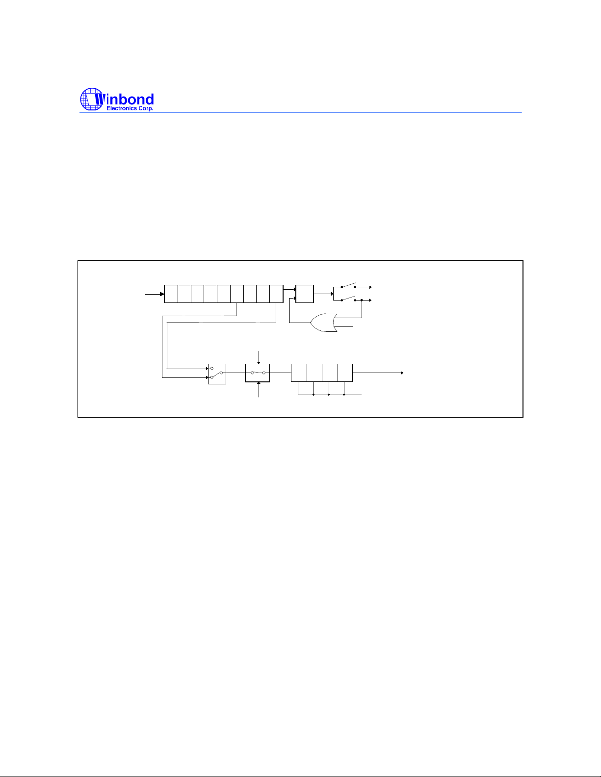
6.11 Watchdog Timer (WDT)
The watchdog timer (WDT) is organized as a 4-bit up counter designed to prevent the program from
unknown errors. When the corresponding option code bit of the WDT set to 1, the WDT is enabled,
and if the WDT overflows, the chip will be reset. At initial reset, the input clock of the WDT is
FOSC/2048. The input clock of the WDT can be switched to FOSC/16384 (or FOSC/2048) by setting
SCR.2 to 1 (or clearing SCR.2 to 0). The contents of the WDT can be reset by the instruction CLR
WDT. In normal operation, the application program must reset WDT before it overflows. A WDT
overflow indicates that operation is not under control and the chip will be reset. The WDT overflow
period is 1S when the system clock (FOSC) is 32 KHz and WDT clock input is FOSC/2048. When the
corresponding option code bit of the WDT set to 0, the WDT function is disabled. The organization of
the Divider0 and watchdog timer is shown in Figure 6-5.
Divider0
Fosc
Q1 Q2 Q9 Q10 Q11 Q12 Q14Q13
...
Fosc/16384
Fosc/2048
SCR.2
Figure 6-5 Organization of Divider0 and watchdog timer
Option code is reset to "0"
Disable
Enable
Option code is set to "1"
Q
R
WDT
Qw1 Qw2
EVF.0
Qw3
HEF.0
IEF.0
1. Reset
2. CLR EVF,#01H
3. CLR DIVR0
Overflow signal
Qw4
1. Reset
Hold mode release (HCF.0)
Divider interrupt (INT0)
System Reset
2. CLR WDT
6.12 Timer/Counter
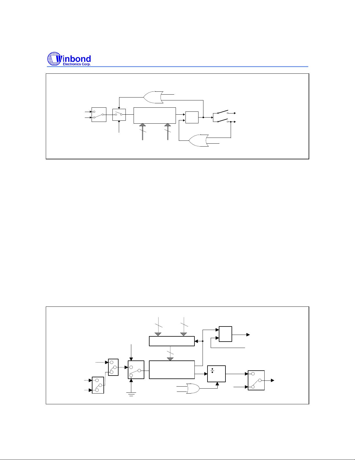
6.12.1 Timer 0 (TM0)
Timer 0 (TM0) is a programmable 8-bit binary down-counter. The specified value can be loaded into
TM0 by executing the MOV TM0L(TM0H),R instructions. When the MOV TM0L(TMOH),R instructions
are executed, it will stop the TM0 down-counting (if the TM0 is down-counting) and reset the MR0.3 to
0, and the specified value can be loaded into TM0. We can then set MR0.3 to 1; this will cause the
event flag 1 (EVF.1) to be reset, and the TM0 will start to count. When it decrements to FFH, Timer 0
stops operating and generates an underflow (EVF.1 = 1). Then, if the Timer 0 interrupt enable flag
has been set (IEF.1 = 1), the interrupt is executed, while if the hold release enable flag 1 has been set
(HEF.1 = 1), the hold state is terminated. The Timer 0 clock input can be set as FOSC/1024 or FOSC/4
by setting MR0.0 to 1 or resetting MR0.0 to 0. The default timer value is FOSC/4. The organization of
Timer 0 is shown in Figure 6-6.
If the Timer 0 clock input is FOSC/4:
Desired Timer 0 interval = (preset value +1) × 4 × 1/ FOSC
If the Timer 0 clock input is FOSC/1024:
Desired Timer 0 interval = (preset value +1) × 1024 × 1/ FOSC
Preset value: Decimal number of Timer 0 preset value
FOSC: Clock oscillation frequency
Publication Release Date: May 1999
- 15 - Revision A1
Page 16
Preliminary W742C810
1. Reset
2. CLR EVF,#02H
3. Reset MR0.3 to 0
4.MOV TM0L,R or MOV TM0H,R
MR0.0
Fosc/1024
Fosc/4
Disable
Enable
Set MR0.3 to 1
MOV TM0H,R MOV TM0L,R
8-Bit Binary
Down Counter
(Timer 0)
4
4
Figure 6-6 Organization of Timer 0
S
Q
R
EVF.1
HEF.1
IEF.1
Hold mode release (HCF.1)
Timer 0 interrupt (INT1)
1. Reset
2. CLR EVF,#02H
3.Set MR0.3 to 1
6.12.2 Timer 1 (TM1)
Timer 1 (TM1) is also a programmable 8-bit binary down counter, as shown in Figure 6-7. Timer 1 can
be used as to output an arbitrary frequency to the MFP pin. The input clock of Timer 1 can be one of
three sources: FOSC/64, FOSC or FS. The source can be selected by setting bit 0 and bit1 of mode
register 1 (MR1). At initial reset, the Timer 1 clock input is FOSC. When the MOV TM1L, R or MOV
TM1H,R instruction is executed, the specified data are loaded into the auto-reload buffer and the TM1
down-counting will keep going on. If the bit 3 of MR1 is set (MR1.3 = 1), the content of the autoreload buffer will be loaded into the TM1 down counter, Timer 1 starts to down count, and the event
flag 7 is reset (EVF.7 = 0). When the timer decrements to FFH, it will generate an underflow (EVF.7 =
1) and be auto-reloaded with the specified data, after which it will continue to count down. Then, if
interrupt enable flag 7 has been set to 1 (IEF.7 = 1), an interrupt is executed; if hold mode release
enable flag 7 is set to 1 (HEF.7 = 1), the hold state is terminated. The specified frequency of Timer 1
can be delivered to the MFP output pin by programming bit2 of MR1. Bit 3 of MR1 can be used to
make Timer 1 stop or start counting.
In a case where Timer 1 clock input is FT:
Desired Timer 1 interval = (preset value +1) / FT
Desired frequency for MFP output pin = FT ÷ (preset value + 1) ÷ 2 (Hz)
Preset value: Decimal number of Timer 1 preset value
FOSC: Clock oscillation frequency
Fosc/64
Fosc
Fs
MR1.0
Set MR1.3 to 1
F
MR1.1
T
MOV TM1H,R
4
Auto-reload buffer
Enable
8-Bit Binary
Down Counter
Disable
Set MR1.3 to 1
Figure 6-7 Organization of Timer 1
MOV TM1L,R
4
8 bits
(Timer 1)
Reset
- 16 -
S
Q
R
Underflow signal
2
circuit
Reset
MFP signal
EVF.7
1. Reset
2. INT7 accept
3. CLR EVF, #80H
4. Set MR1.3 to 1
MFP
output pin
MR1.2
Page 17
Preliminary W742C810
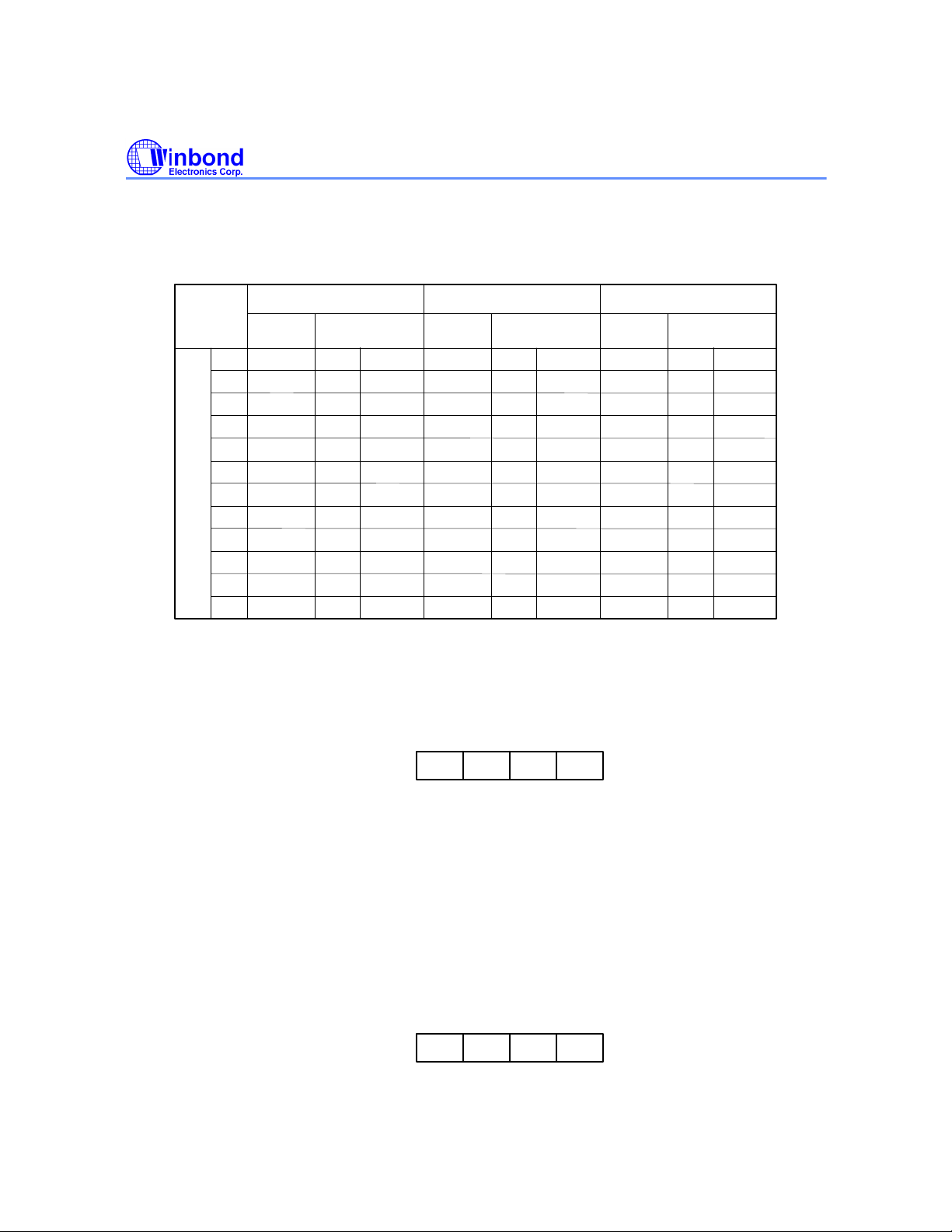
For example, when FT equals 32768 Hz, depending on the preset value of TM1, the MFP pin will
output a single tone signal in the tone frequency range from 64 Hz to 16384 Hz. The relation between
the tone frequency and the preset value of TM1 is shown in the table below.
Table2 The relation between the tone frequency and the preset value of TM1
3rd octave 4th octave 5th octave
Tone
frequency
C
130.81
#
C
138.59
D
T
O
N
E
Note: Central tone is A4 (440 Hz).
146.83
#
D
155.56
E
164.81
F
174.61
#
F
185.00
G
196.00
#
G
207.65
A
220.00
#
A
233.08
B
246.94
TM1 preset value
& MFP frequency
7CH
131.07
75H
138.84
6FH
146.28
68H
156.03
62H
165.49
5DH
174.30
58H
184.09
53H
195.04
4EH
207.39
49H
221.40
45H
234.05
41H
248.24
Tone
frequency
261.63
277.18
293.66
311.13
329.63
349.23
369.99
392.00
415.30
440.00
466.16
493.88
TM1 preset value
& MFP frequency
260.06
3EH
277.69
3AH
292.57
37H
309.13
34H
327.68
31H
372.36
2EH
390.09
2BH
420.10
29H
443.81
26H
442.81
24H
22H
468.11
20H
496.48
Tone
frequency
523.25
554.37
587.33
622.25
659.26
698.46
739.99
783.99
830.61
880.00
932.23
987.77
TM1 preset value
& MFP frequency
1EH
528.51
1CH
564.96
1BH
585.14
19H
630.15
18H
655.36
16H
712.34
15H
744.72
14H
780.19
13H
819.20
12H
862.84
11H
910.22
10H
963.76
6.12.3 Mode Register 0 (MR0)
Mode Register 0 is organized as a 4-bit binary register (MR0.0 to MR0.3). MR0 can be used to
control the operation of Timer 0. The bit descriptions are as follows:
0123
Note: W means write only.
MR0
W
W
W W
Bit 0 = 0 The fundamental frequency of Timer 0 is FOSC/4.
= 1 The fundamental frequency of Timer 0 is FOSC/1024.
Bit 1 & Bit 2 are reserved
Bit 3 = 0 Timer 0 stops down-counting.
= 1 Timer 0 starts down-counting.
6.12.4 Mode Register 1 (MR1)
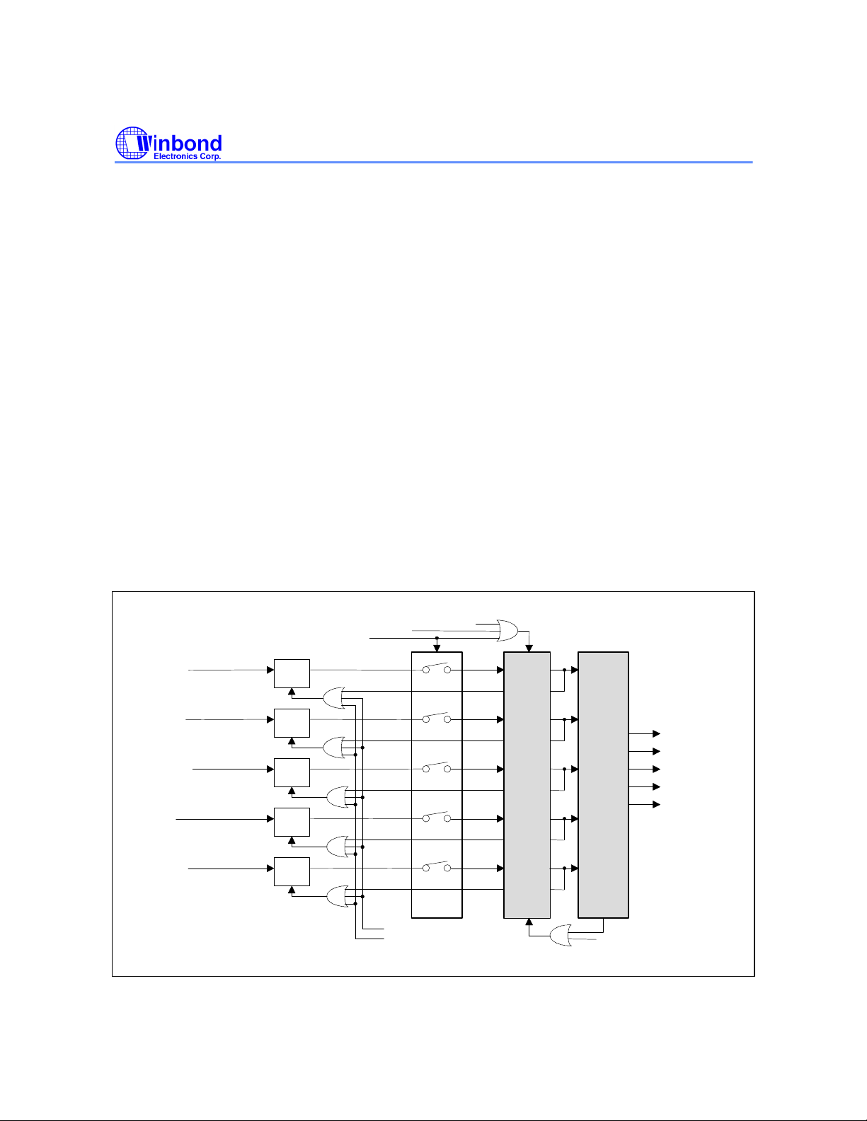
Mode Register 1 is organized as a 4-bit binary register (MR1.0 to MR1.3). MR1 can be used to control
the operation of Timer 1. The bit descriptions are as follows:
0123
MR1
Note: W means write only.
WW W W
Publication Release Date: May 1999
- 17 - Revision A1
Page 18
Preliminary W742C810
Disable
Bit 0 = 0 The internal fundamental frequency of Timer 1 is FOSC.
= 1 The internal fundamental frequency of Timer 1 is FOSC/64.
Bit 1 = 0 The fundamental frequency source of Timer 1 is the internal clock.
= 1 The fundamental frequency source of Timer 1 is the sub-oscillator frequency FS
(32.768 KHz).
Bit 2 = 0 The specified waveform of the MFP generator is delivered at the MFP pin.
= 1 The specified frequency of Timer 1 is delivered at MFP pin.
Bit 3 = 0 Timer 1 stops down-counting.
= 1 Timer 1 starts down-counting.
6.13 Interrupts
The W742C810 provides four internal interrupt sources (Divider 0, Divider 1, Timer 0, Timer 1) and
one external interrupt source (port RC). Vector addresses for each of the interrupts are located in the
range of program memory (ROM) addresses 004H to 020H. The flags IEF, PEF, and EVF are used to
control the interrupts. When EVF is set to "1" by hardware and the corresponding bits of IEF and PEF
have been set by software, an interrupt is generated. When an interrupt occurs, all of the interrupts
are inhibited until the EN INT or MOV IEF,#I instruction is invoked. The interrupts can also be
disabled by executing the DIS INT instruction. When an interrupt is generated in hold mode, the hold
mode will be released momentarily and interrupt subroutine will be executed. After the RTN
instruction is executed in an interrupt subroutine, the µC will enter hold mode again. The operation
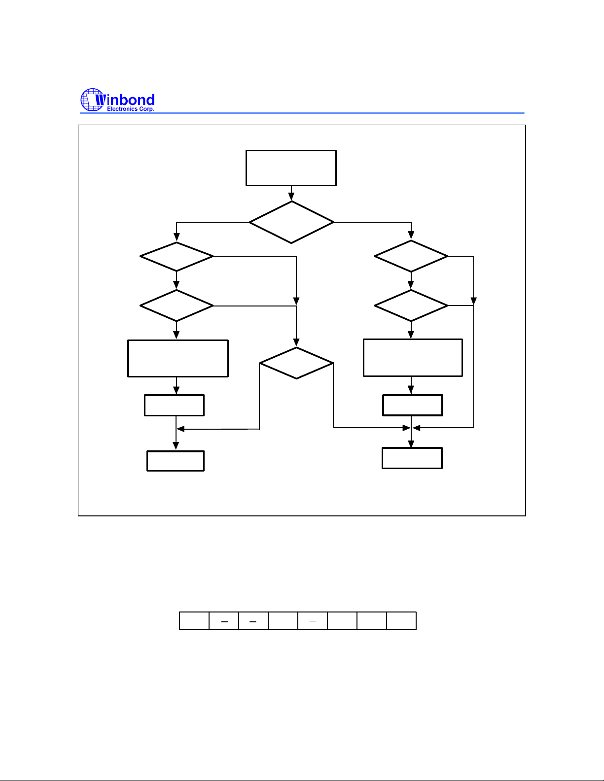
flow chart is shown in Figure 6-9. The control diagram is shown below.
Divider 0
overflow signal
Timer 0
underflow signal
Port RC
signal change
Divider 1
overflow signal
Timer 1
underflow signal
SRQ
SRQ
SRQ
SRQ
SRQ
Initial Reset
EN INT
MOV IEF, #I
EVF.0
IEF.0
EVF.1
IEF.1
EVF.2
IEF.2
EVF.4
IEF.4
EVF.7
IEF.7
Initial Reset
CLR EVF, #I instruction
Figure 6-8 Interrupt event control duagram
Interrupt
Process
Circuit
Enable
Interrupt
Vector
Generator
DIS INT instruction
004H
008H
00CH
014H
020H
- 18 -
Page 19

Preliminary W742C810
6.14 Stop Mode Operation
In stop mode, all operations of the µC cease (excluding the operation of the sub-oscillator and Divider
1 and LCD driver), and MFP pin is kept to high state. The µC enters stop mode when the STOP
instruction is executed and exits stop mode when an external trigger is activated (by a falling signal
on the RC). When the designated signal is accepted, the µC awakens and executes the next
instruction. To prevent erroneous execution, the NOP instruction should follow the STOP command.
However, in the dual-clock slow operation mode, the STOP instruction will disable the main-oscillator;
the µC system is still operated by the sub-oscillator.
6.14.1 Stop Mode Wake-up Enable Flag for RC Port (SEF)
The stop mode wake-up flag for port RC is organized as a 4-bit binary register (SEF.0 to SEF.3).
Before port RC may be used to make the device exit the stop mode, the content of the SEF must be
set first. The SEF is controlled by the MOV SEF, #I instruction. The bit descriptions are as follows:
3
Note: W means write only.
SEF.0 = 1 Device will exit stop mode when falling edge signal is applied to pin RC.0
SEF.1 = 1 Device will exit stop mode when falling edge signal is applied to pin RC.1
SEF.2 = 1 Device will exit stop mode when falling edge signal is applied to pin RC.2
SEF.3 = 1 Device will exit stop mode when falling edge signal is applied to pin RC.3
SEF w w w
012
w
6.15 Hold Mode Operation
In hold mode, all operations of the µC cease, except for the operation of the oscillator, Timer, Divider,
LCD driver, DTMF generator and MFP generator. The µC enters hold mode when the HOLD
instruction is executed. The hold mode can be released in one of five ways: by the action of timer 0,
timer 1, divider 0, divider 1, or the RC port. Before the device enters the hold mode, the HEF, PEF,
and IEF flags must be set to define the hold mode release conditions. For more details, refer to the
instruction-set table and the following flow chart.
Publication Release Date: May 1999
- 19 - Revision A1
Page 20
Divider 0, Divider 1, Timer
0, Timer 1, Signal Change
at RC Port
Preliminary W742C810
In
HOLD
Mode?
Interrupt
Enable?
Yes
IEF
Flag Set?
Yes
Reset EVF Flag
Execute
Interrupt Service Routine
(Note)
Disable interrupt
HOLD
Note: The bit of EVF corresponding to the interrupt signal will be reset.
No
HEF
Flag Set?
NoYes
Interrupt
Enable?
Yes
IEF
Flag Set?
Yes
Reset EVF Flag
Execute
Interrupt Service Routine
YesNo
Disable interrupt
PC <- (PC+1)
NoNo
No
(Note)
Figure 6-9 Hold Mode and Interrupt Operation Flow Chart
6.15.1 Hold Mode Release Enable Flag (HEF)
The hold mode release enable flag is organized as an 8-bit binary register (HEF.0 to HEF.7). The
HEF is used to control the hold mode release conditions. It is controlled by the MOV HEF, #I
instruction. The bit descriptions are as follows:
012
Note: W means write only.
HEF w w w w
34567
w
HEF.0 = 1 Overflow from the Divider 0 causes Hold mode to be released.
HEF.1 = 1 Underflow from Timer 0 causes Hold mode to be released.
HEF.2 = 1 Signal change at port RC causes Hold mode to be released.
- 20 -
Page 21
Preliminary W742C810
HEF.3 is reserved.
HEF.4 = 1 Overflow from the Divider 1 causes Hold mode to be released.
HEF.5 & HEF.6 are reserved.
HEF.7 = 1 Underflow from Timer 1 causes Hold mode to be released.
6.15.2 Interrupt Enable Flag (IEF)
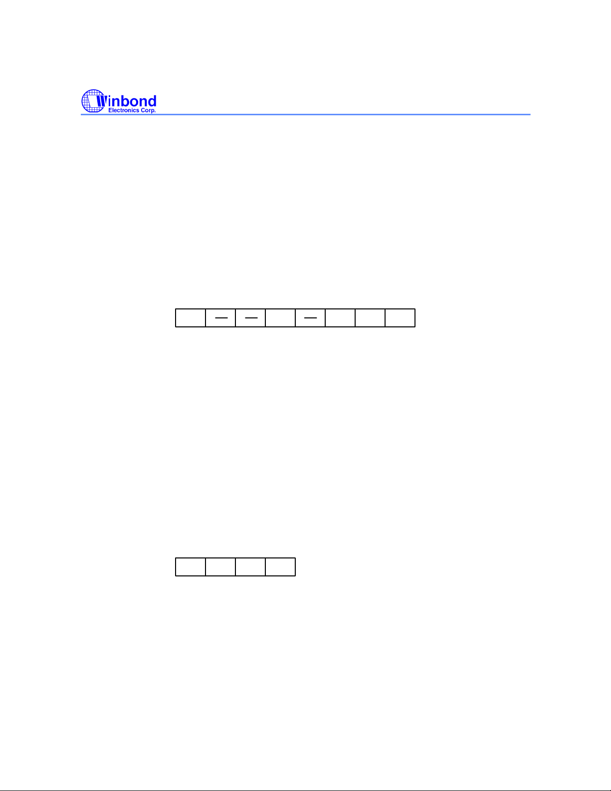
The interrupt enable flag is organized as an 8-bit binary register (IEF.0 to IEF.7). These bits are used
to control the interrupt conditions. It is controlled by the MOV IEF, #I instruction. When one of these
interrupts is accepted, the corresponding bit of the event flag will be reset, but the other bits are
unaffected. In interrupt subroutine, these interrupts will be disabled till the instruction MOV IEF, #I or
EN INT is executed again. Otherwise, these interrupts can be disabled by executing DIS INT
instruction. The bit descriptions are as follows:
4
7
Note: W means write only.
IEF.0 = 1 Interrupt 0 is accepted by overflow from the Divider 0.
IEF.1 = 1 Interrupt 1 is accepted by underflow from the Timer 0.
IEF.2 = 1 Interrupt 2 is accepted by a signal change at port RC.
IEF.3 is reserved.
IEF.4 = 1 Interrupt 0 is accepted by overflow from the Divider 1.
IEF.5 & IEF.6 are reserved.
IEF.7 = 1 Interrupt 7 is accepted by underflow from Timer 1.
6.15.3 Port Enable Flag (PEF)
The port enable flag is organized as a 4-bit binary register (PEF.0 to PEF.3). Before port RC may be
used to release the hold mode or preform interrupt function, the content of the PEF must be set first.
The PEF is controlled by the MOV PEF, #I instruction. The bit descriptions are as follows:
IEF
3
PEF w w w
56 0
w
012
w
w w
123
ww
Note: W means write only.
PEF.0: Enable/disable the signal change at pin RC.0 to release hold mode or perform interrupt.
PEF.1: Enable/disable the signal change at pin RC.1 to release hold mode or perform interrupt.
PEF.2: Enable/disable the signal change at pin RC.2 to release hold mode or perform interrupt.
PEF.3: Enable/disable the signal change at pin RC.3 to release hold mode or perform interrupt.
Publication Release Date: May 1999
- 21 - Revision A1
Page 22
Preliminary W742C810
6.15.4 Hold Mode Release Condition Flag (HCF)
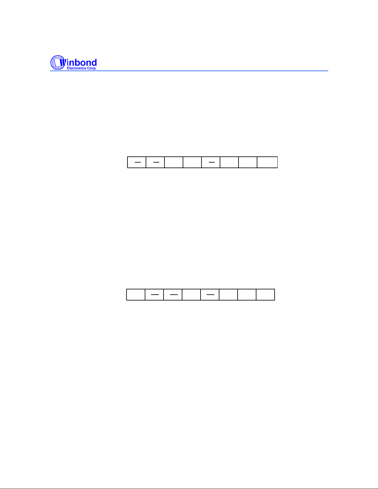
The hold mode release condition flag is organized as an 8-bit binary register (HCF.0 to HCF.7). It
indicates by which interrupt source the hold mode has been released, and is loaded by hardware. The
HCF can be read out by the MOVA R, HCFL and MOVA R, HCFH instructions. When any of the HCF
bits is "1," the hold mode will be released and the HOLD instruction is invalid. The HCF can be reset
by the CLR EVF or MOV HEF,#I (HEF = 0) instructions. When EVF and HEF have been reset, the
corresponding bit of HCF is reset simultaneously. The bit descriptions are as follows:
67
R RHCF
Note: R means read only.
HCF.0 = 1 Hold mode was released by overflow from the divider 0.
HCF.1 = 1 Hold mode was released by underflow from the timer 0.
HCF.2 = 1 Hold mode was released by a signal change at port RC.
HCF.3 is reserved.
HCF.4 = 1 Hold mode was released by overflow from the divider 1.
HCF.5 = 1 Hold mode was released by underflow from the timer 1.
HCF.6 and HCF.7 are reserved.
6.15.5 Event Flag (EVF)
The event flag is organized as an 8-bit binary register (EVF.0 to EVF.7). It is set by hardware and
reset by CLR EVF,#I instruction or the occurrence of an interrupt. The bit descriptions are as follows:
67
EVF
Note: W means write only.
EVF.0 = 1 Overflow from divider 0 occurred.
EVF.1 = 1 Underflow from timer 0 occurred.
EVF.2 = 1 Signal change at port RC occurred.
EVF.3 is reserved.
EVF.4 = 1 Overflow from divider 1 occurred.
EVF.5 & EVF.6 are reserved.
EVF.7 = 1 Underflow from Timer 1 occurred.
W
W W
R R R
W
012345
012345
W
- 22 -
Page 23
Preliminary W742C810
6.16 Reset Function
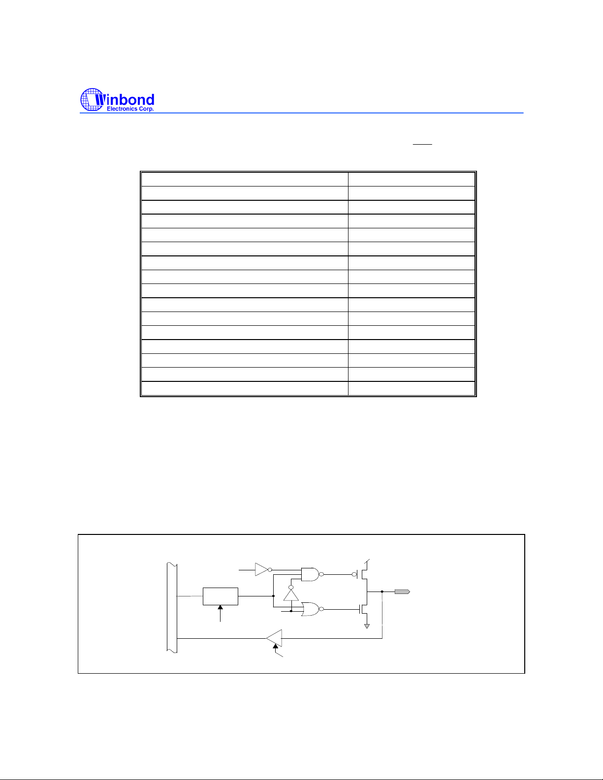
The W742C810 is reset either by a power-on reset or by using the external RES pin. The initial state
of the W742C810 after the reset function is executed is described below.
Program Counter (PC) 000H
TM0, TM1 Reset
MR0, MR1, PAGE registers Reset
PSR0, SCR registers Reset
IEF, HEF, HCF, PEF, EVF, SEF flags Reset
WRP, DBKR register Reset
Timer 0 input clock FOSC/4
Timer 1 input clock FOSC
MFP output Low
DTMF output Hi-Z
Input/output ports RA,RB, RD Input mode
Output port RE & RF High
RA, RB & RD ports output type CMOS type
RC ports pull-high resistors Disable
Input clock of the watchdog timer FOSC/2048
LCD display OFF
Table 3 The initial state after the reset function is executed
6.17 Input/Output Ports RA, RB & RD
Port RA consists of pins RA.0 to RA.3. Port RB consists of pins RB.0 to RB.3. Port RD consists of
pins RD.0 to RD.3. At initial reset, input/output ports RA, RB and RD are all in input mode. When RA,
RB are used as output ports, CMOS or NMOS open drain output type can be selected by the PM0
register. But when RD is used as output port, the output type is just fixed to be CMOS output type.
Each pin of port RA, RB and RD can be specified as input or output mode independently by the PM1,
PM2 and PM5 registers. The MOVA R, RA or MOVA R, RB or MOVA R, RD instructions operate the
input functions and the MOV RA, R or MOV RB, R or MOV RD, R operate the output functions. For
more details, refer to the instruction table and Figure 6-10 and Figure 6-11.
Input/Output Pin of the RA(RB)
PM0.0(PM0.1)
I/O PIN
RA.n(RB.n)
DATA
BUS
Output
Buffer
Enable
MOV RA,R(MOV RB,R)
instruction
PM1.n (PM2.n)
Enable
MOVA R,RA(MOVA R,RB) instruction
Figure 6-10 Architecture of RA (RB) Input/Output Pins
- 23 - Revision A1
Publication Release Date: May 1999
Page 24
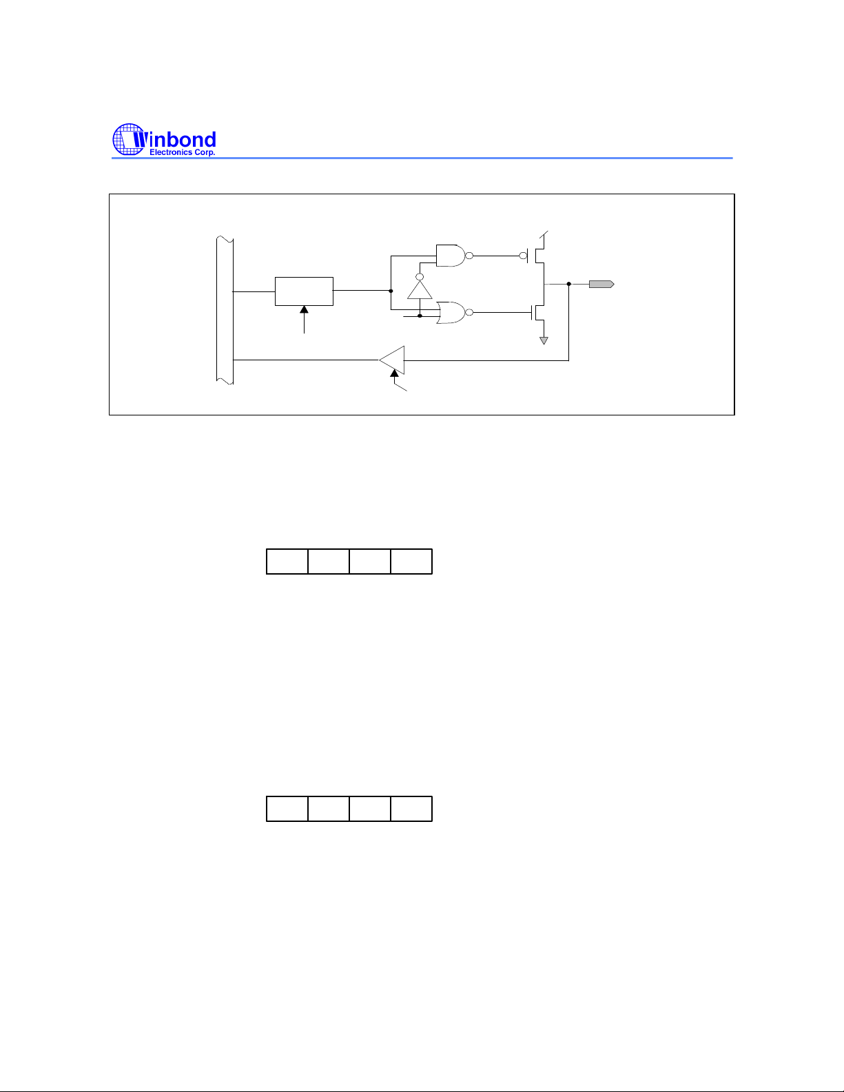
Input/Output Pin of the RD
Preliminary W742C810
I/O PIN
RD.n
DATA
BUS
Output
Buffer
Enable
MOV RD,R instruction
Figure 6-11 Architecture of RD Input/Output pins
PM5.n
Enable
MOVA R,RD instruction
6.17.1 Port Mode 0 Register (PM0)
The port mode 0 register is organized as a 4-bit binary register (PM0.0 to PM0.3). PM0 can be used
to determine the structure of the input/output ports; it is controlled by the MOV PM0, #I instruction.
The bit descriptions are as follows:
012
w
Note: W means write only.
3
PM0 w w w
Bit 0 = 0 RA port is CMOS output type. Bit 0 = 1 RA port is NMOS open drain output type.
Bit 1 = 0 RB port is CMOS output type. Bit 1 = 1 RB port is NMOS open drain output type.
Bit 2 = 0 RC port pull-high resistor is disabled. Bit 2 = 1 RC port pull-high resistor is enabled.
Bit 3 is reserved.
6.17.2 Port Mode 1 Register (PM1)
The port mode 1 register is organized as a 4-bit binary register (PM1.0 to PM1.3). PM1 can be used
to control the input/output mode of port RA. PM1 is controlled by the MOV PM1, #I instruction. The bit
descriptions are as follows:
012
w
Note: W means write only.
3
PM1 w w w
Bit 0 = 0 RA.0 works as output pin; Bit 0 = 1 RA.0 works as input pin
Bit 1 = 0 RA.1 works as output pin; Bit 1 = 1 RA.1 works as input pin
Bit 2 = 0 RA.2 works as output pin; Bit 2 = 1 RA.2 works as input pin
Bit 3 = 0 RA.3 works as output pin; Bit 3 = 1 RA.3 works as input pin
At initial reset, port RA is input mode (PM1 = 1111B).
- 24 -
Page 25
Preliminary W742C810
6.17.3 Port Mode 2 Register (PM2)
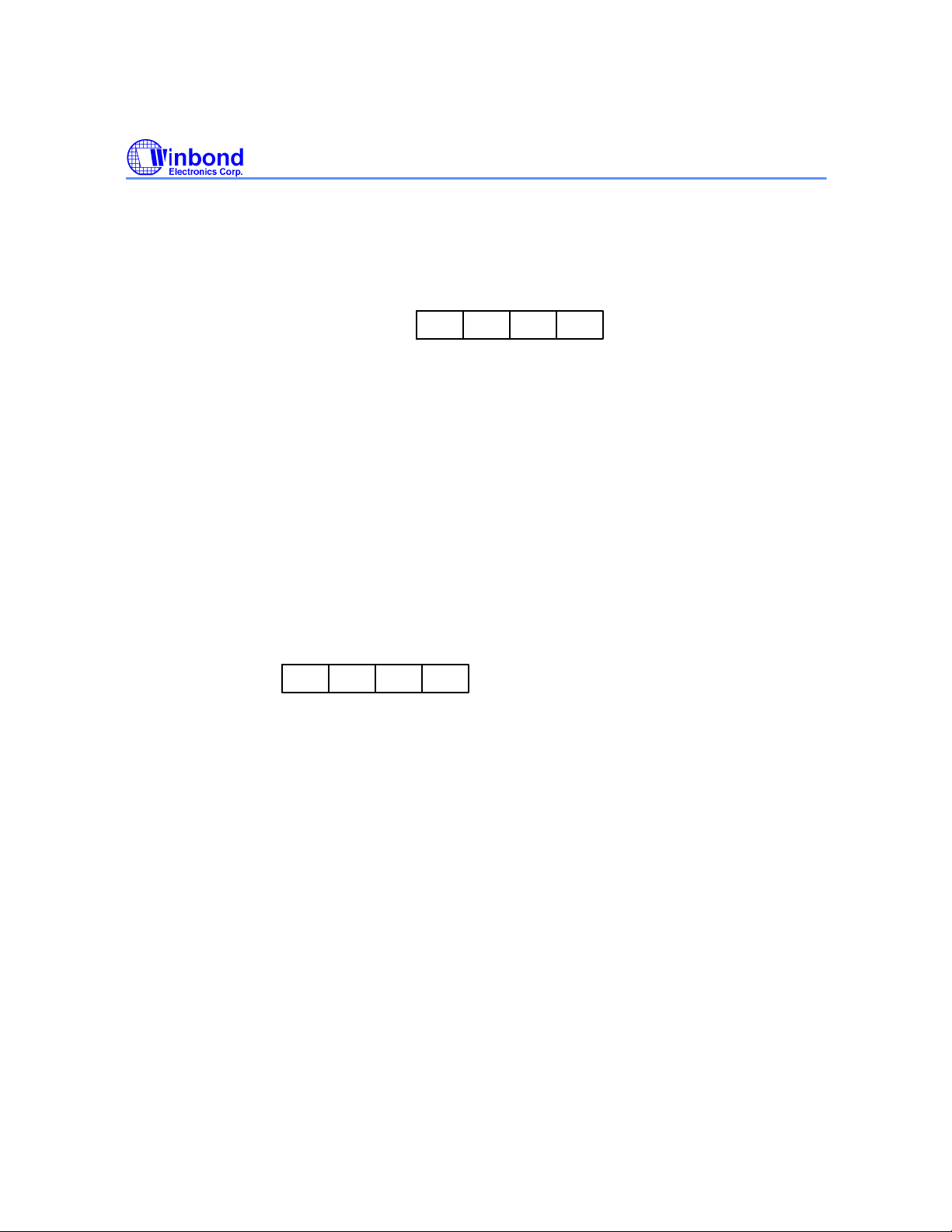
The port mode 2 register is organized as a 4-bit binary register (PM2.0 to PM2.3). PM2 can be used
to control the input/output mode of port RB. PM2 is controlled by the MOV PM2, #I instruction. The bit
descriptions are as follows:
3
PM2 w w w
Note: W means write only.
Bit 0 = 0 RB.0 works as output pin; Bit 0 = 1 RB.0 works as input pin
Bit 1 = 0 RB.1 works as output pin; Bit 1 = 1 RB.1 works as input pin
Bit 2 = 0 RB.2 works as output pin; Bit 2 = 1 RB.2 works as input pin
Bit 3 = 0 RB.3 works as output pin; Bit 3 = 1 RB.3 works as input pin
At initial reset, the port RB is input mode (PM2 = 1111B).
6.17.4 Port Mode 5 Register (PM5)
The port mode 5 register is organized as a 4-bit binary register (PM5.0 to PM5.3). PM5 can be used
to control the input/output mode of port RD. PM5 is controlled by the MOV PM5, #I instruction. The bit
descriptions are as follows:
3
Note: W means write only.
Bit 0 = 0 RD.0 works as output pin; Bit 0 = 1 RD.0 works as input pin
Bit 1 = 0 RD.1 works as output pin; Bit 1 = 1 RD.1 works as input pin
Bit 2 = 0 RD.2 works as output pin; Bit 2 = 1 RD.2 works as input pin
Bit 3 = 0 RD.3 works as output pin; Bit 3 = 1 RD.3 works as input pin
PM5 w w w
012
w
012
w
At initial reset, the port RD is input mode (PM5 = 1111B).
6.18 Input Ports RC
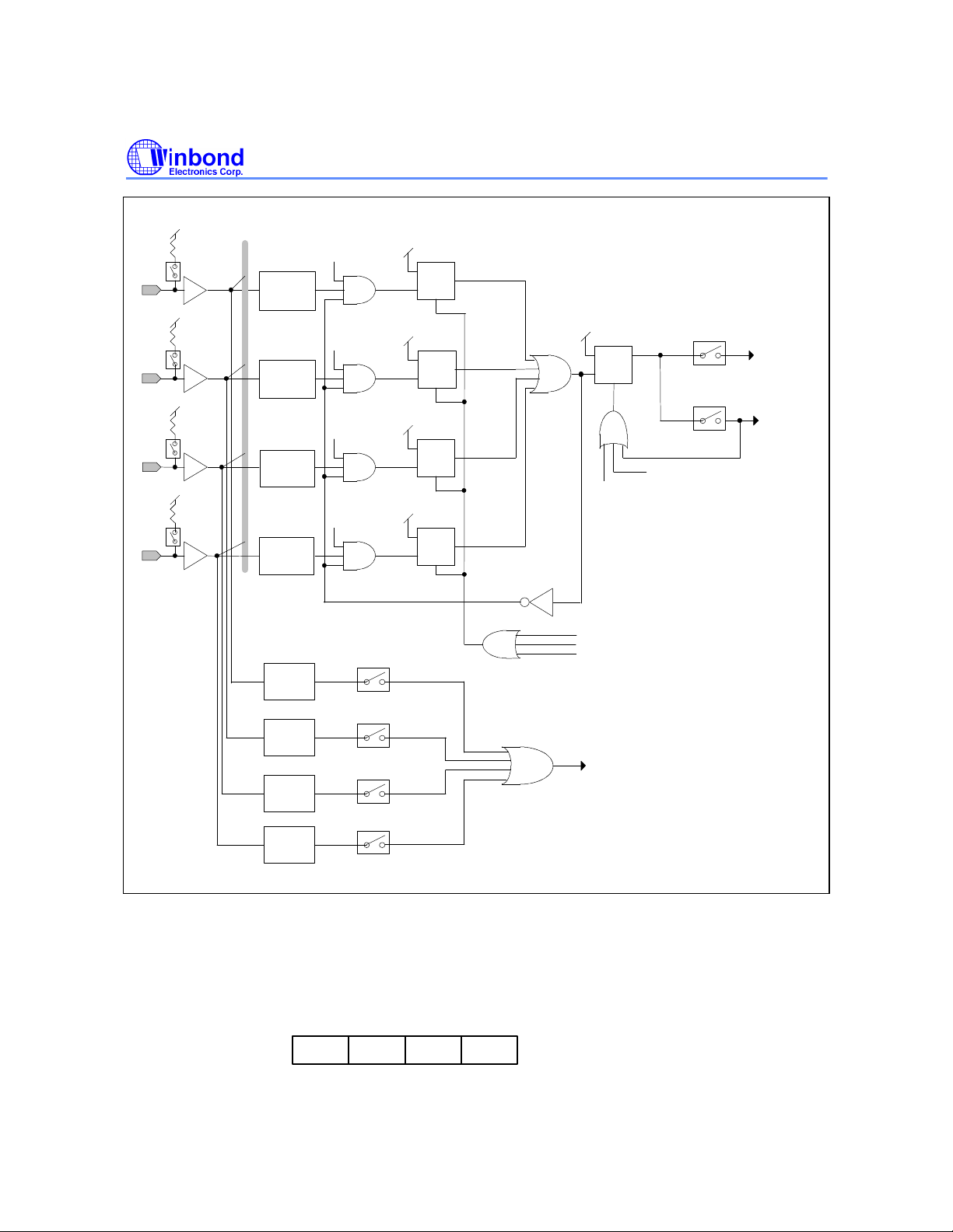
Port RC consists of pins RC.0 to RC.3. Each pin of port RC can be connected to a pull-up resistor,
which is controlled by the port mode 0 register(PM0). When the PEF, HEF, and IEF corresponding to
the RC port are set, a signal change at the specified pins of port RC will execute the hold mode
release or interrupt subroutine. Port status register 0 (PSR0) records the status of ports RC, i.e., any
signal changes on the pins that make up the ports. PSR0 can be read out and cleared by the MOV R,
PSR0, and CLR PSR0 instructions. In addition, the falling edge signal on the pin of port RC specified
by the instruction MOV SEF, #I will cause the device to exit the stop mode. Refer to Figure 6-12 and
the instruction table for more details.
Publication Release Date: May 1999
- 25 - Revision A1
Page 26
RC.0
PM0.2
DATA BUS
Signal
change
detector
PEF.0
Preliminary W742C810
PSR0.0
D
Q
ck
R
RC.1
RC.2
RC.3
PM0.2
PM0.2
PM0.2
Signal
change
detector
Signal
change
detector
Signal
change
detector
Falling
Edge
detector
Falling
Edge
detector
Falling
Edge
detector
Falling
Edge
detector
PEF.1
PEF.2
PEF.3
SEF.0
SEF.1
SEF.2
SEF.3
EVF.2
D
ck
PSR0.1
Q
R
D
Q
ck
R
HEF.2
HCF.2
IEF.2
INT 2
PSR0.2
D
Q
ck
R
CLR EVF, #I
Reset
D
ck
PSR0.3
Q
R
Reset
MOV PEF, #I
CLR PSR0
To Wake Up Stop Mode
Figure 6-12 Architecture of Input Ports RC
6.18.1 Port Status Register 0 (PSR0)
Port status register 0 is organized as a 4-bit binary register (PSR0.0 to PSR0.3). PSR0 can be read or
cleared by the MOVA R, PSR0, and CLR PSR0 instructions. The bit descriptions are as follows:
0123
PSR0
Note: R means read only.
RR R R
- 26 -
Page 27
Preliminary W742C810
Bit 0 = 1 Signal change at RC.0
Bit 1 = 1 Signal change at RC.1
Bit 2 = 1 Signal change at RC.2
Bit 3 = 1 Signal change at RC.3
6.19 Output Port RE & RF
Output port RE is used as an output of the internal RT port. When the MOV RE, R instruction is
executed, the data in the RAM will be output to port RT through port RE. It provides a high sink
current to drive an LED. RF port is just used as an output port. When the MOV RF, R instruction is
executed, the data in the RAM will be output to RF.
6.20 DTMF Output Pin (DTMF)
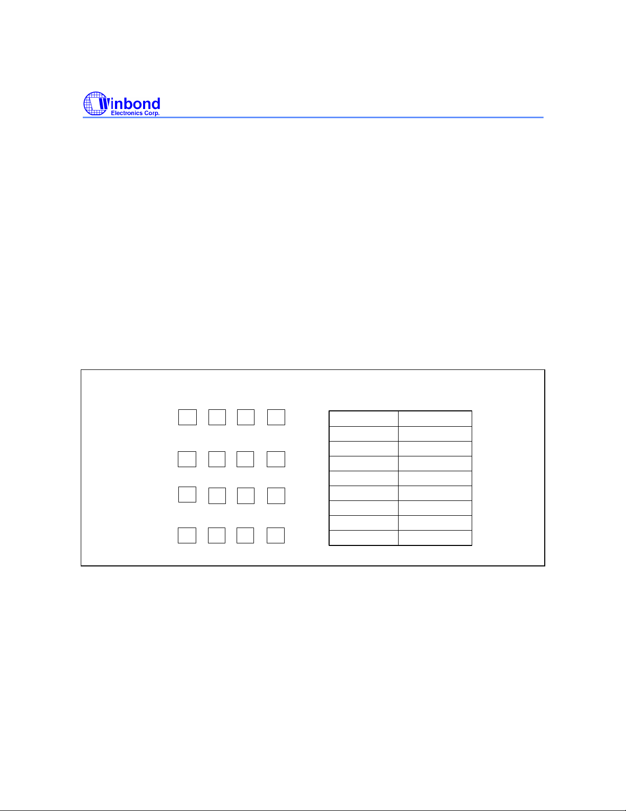
This pin should output the dual tone multi-frequency signal from the DTMF generator. There is a
DTMF register that can specify the wanted low/high frequency, and the Dual Tone Control Register
(DTCR) can control whether the dual tone will be output or not. The tones are divided into two groups
(low group and high group); one tone from each group is selected to represent a digit. The relation
between the DTMF signal and the corresponding touch tone keypad is shown in Figure 6-13.
C1
R1
R2
R3
R4
C2 C3 C4
1 2 3 A
4 5 6 B
7
8
0 # D
*
Figure 6-13 The relation between the touch tone keypad and the frequency
C
9
Row/Col Frequency
R1 697 Hz
R2 770 Hz
R3 852 Hz
R4 941 Hz
C1 1209 Hz
C2 1336 Hz
C3 1477 Hz
C4 1633 Hz
Publication Release Date: May 1999
- 27 - Revision A1
Page 28
Preliminary W742C810
6.20.1 DTMF register
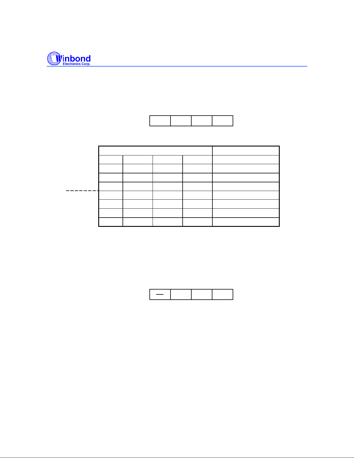
DTMF register is organized as a 4-bit binary register. By controlling the DTMF register, one tone of
the low/high group can be selected. The MOV DTMF,R instruction can specify the wanted tones. The
bit descriptions are as follows:
0123
DTMF
Note: W means write only.
b3 b2 b1 b0 Selected tone
X X 0 0 1209 Hz
High
group
Low
group
Note: X means this bit do not care.
6.20.2 Dual Tone Control Register (DTCR)
Dual tone control register is organized as a 4-bit binary register. The output of the dual or single tone
will be controlled by this register. The MOV DTCR,#I instruction can specify the wanted status. The bit
descriptions are as follows:
X X 0 1 1336 Hz
X X 1 0 1477 Hz
X X 1 1 1633 Hz
0 0 X X 697 Hz
0 1 X X 770 Hz
1 0 X X 852 Hz
1 1 X X 941 Hz
WW W W
0123
DTCR
Note: W means write only.
Bit 0 = 1 Low group tone output is enabled.
Bit 1 = 1 High group tone output is enabled.
Bit 2 = 1 DTMF output is enabled. When Bit 2 is reset to 0, the DTMF output pin will be Hi-Z state.
Bit 3 is reserved.
W W W
6.21 MFP Output Pin (MFP)
The MFP output pin can output the Timer 1 clock or the modulation frequency; the output of the pin is
determined by mode register 1 (MR1). The organization of MR1 is shown in Figuer 6-7. When bit 2 of
MR1 is reset to "0," the MFP output can deliver a modulation output in any combination of one signal
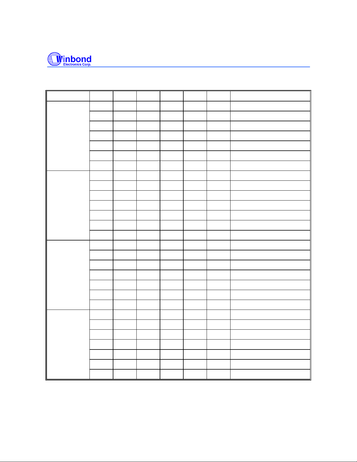
from among DC, 4096Hz, 2048Hz, and one or more signals from among 128 Hz, 64 Hz, 8 Hz, 4 Hz, 2
Hz, or 1 Hz (when using a 32.768 KHz crystal). The MOV MFP, #I instruction is used to specify the
modulation output combination. The data specified by the 8-bit operand and the MFP output pin are
shown on the next page.
- 28 -
Page 29
Preliminary W742C810
Table 4 The relation between the MFP output frequncy and the data specified by 8-bit operand
(Fosc = 32.768 KHz)
R7 R6 R5 R4 R3 R2 R1 R0 FUNCTION
0 0 0 0 0 0 Low level
0 0 0 0 0 1 128 Hz
0 0 0 0 1 0 64 Hz
0 0 0 0 0 1 0 0 8 Hz
0 0 1 0 0 0 4 Hz
0 1 0 0 0 0 2 Hz
1 0 0 0 0 0 1 Hz
0 0 0 0 0 0 High level
0 0 0 0 0 1 128 Hz
0 0 0 0 1 0 64 Hz
0 1 0 0 0 1 0 0 8 Hz
0 0 1 0 0 0 4 Hz
0 1 0 0 0 0 2 Hz
1 0 0 0 0 0 1 Hz
0 0 0 0 0 0 2048 Hz
0 0 0 0 0 1 2048 Hz * 128 Hz
0 0 0 0 1 0 2048 Hz * 64 Hz
1 0 0 0 0 1 0 0 2048 Hz * 8 Hz
0 0 1 0 0 0 2048 Hz * 4 Hz
0 1 0 0 0 0 2048 Hz * 2 Hz
1 0 0 0 0 0 2048 Hz * 1 Hz
0 0 0 0 0 0 4096 Hz
0 0 0 0 0 1 4096 Hz * 128 Hz
0 0 0 0 1 0 4096 Hz * 64 Hz
1 1 0 0 0 1 0 0 4096 Hz * 8 Hz
0 0 1 0 0 0 4096 Hz * 4 Hz
0 1 0 0 0 0 4096 Hz * 2 Hz
1 0 0 0 0 0 4096 Hz * 1 Hz
Publication Release Date: May 1999
- 29 - Revision A1
Page 30
Preliminary W742C810
6.22 LCD Controller/Driver
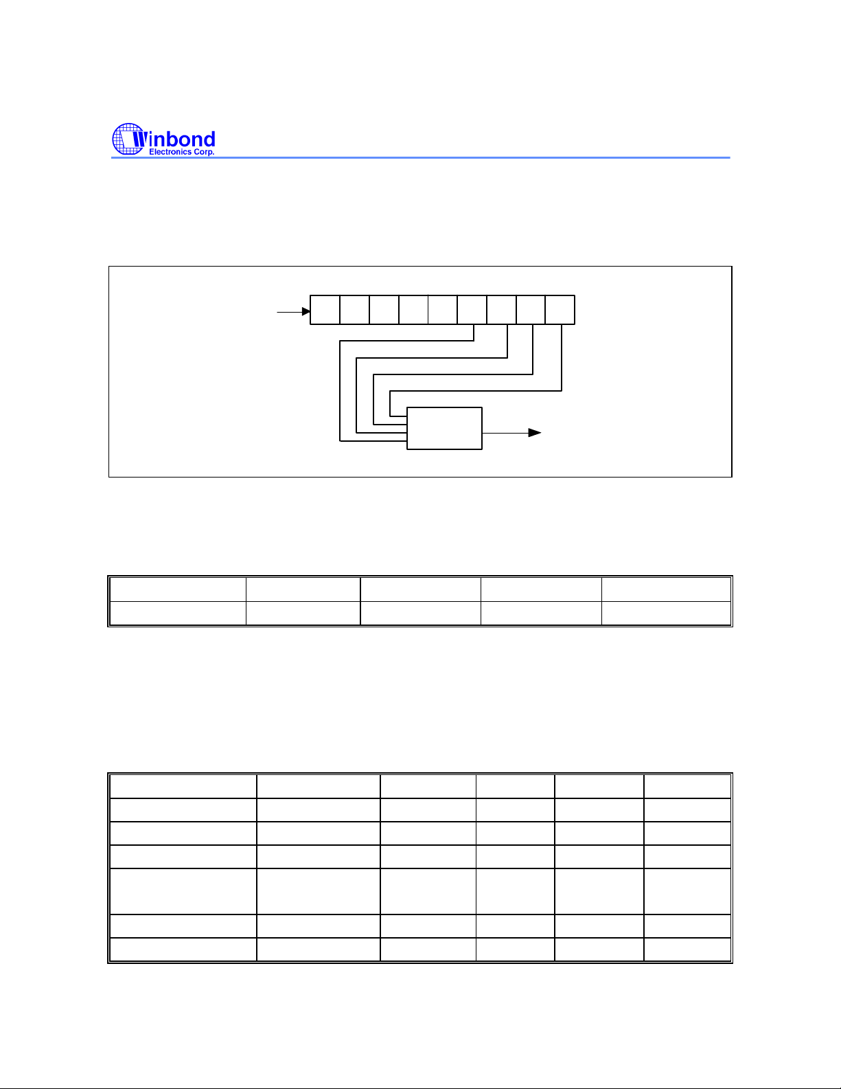
The W742C810 can directly drive an LCD with 40 segment output pins and 4 common output pins for
a total of 40 × 4 dots. The LCD driving mode is 1/3 bias 1/4 duty. The alternating frequency of the
LCD can be set as Fw/64, Fw/128, Fw/256, or Fw/512. The structure of the LCD alternating frequency
(FLCD) is shown in Figure 6-14.
Fw
Sub-oscillator clock
Q1 Q2 Q3 Q4 Q5 Q6 Q7 Q8 Q9
Fw/64
Fw/128
Fw/256
Fw/512
Selector
Figure 6-14 LCD alternating frequency (FLCD) circuit diagram
F
LCD
Fw = 32.768 KHz, the LCD frequency is as shown in the table below.
Table 5 The relartionship between the FLCD and the duty cycle
LCD Frequency
Fw/512 (64 Hz) Fw/256 (128Hz) Fw/128 (256 Hz) Fw/64 (512 Hz)
1/4 duty 16 Hz 32 Hz 64 Hz 128 Hz
Corresponding to the 40 LCD drive output pins, there are 40 LCD data RAM segments. Instructions
such as MOV LPL,R, MOV LPH,R, MOV @LP,R, and MOV R,@LP are used to control the LCD data
RAM. The data in the LCD data RAM are transferred to the segment output pins automatically without
program control. When the bit value of the LCD data RAM is "1," the LCD is turned on. When the bit
value of the LCD data RAM is "0," LCD is turned off. The contents of the LCD data RAM (LCDR) are
sent out through the segment0 to segment39 pins by a direct memory access. The relation between
the LCD data RAM and segment/common pins is shown below.
Table 6 The relation between the LCDR and segment/common pins used as LCD drive output pins
COM3 COM2 COM1 COM0
LCD DATA RAM OUTPUT PIN BIT 3 BIT 2 BIT 1 BIT 0
LCDR00 SEG0 0/1 0/1 0/1 0/1
LCDR01 SEG1 0/1 0/1 0/1 0/1
:
:
:
:
:
:
:
:
:
:
:
:
LCDR26 SEG38 0/1 0/1 0/1 0/1
LCDR27 SEG39 0/1 0/1 0/1 0/1
- 30 -
Page 31
Preliminary W742C810
The LCDON instruction turns on the LCD display (even in HOLD mode), and the LCDOFF instruction
turns off the LCD display. At initial reset, all the LCD segments are unlit. When the initial reset state
ends, the LCD display is turned off automatically. To turn on the LCD display, the instruction LCDON
must be executed.
6.22.1 LCD RAM addressing method
There are 40 LCD RAMs (LCDR00 - LCDR27) that should be indirectly addressed. The LCD RAM
pointer (LP) is used to point to the address of the wanted LCD RAM. The LP is organized as 6-bit
binary register. The MOV LPL,R and MOV LPH,R instructions can load the LCD RAM address to the
LP from R. The MOV @LP,R and MOV R,@LP instructions can access the pointed LCD RAM
content.
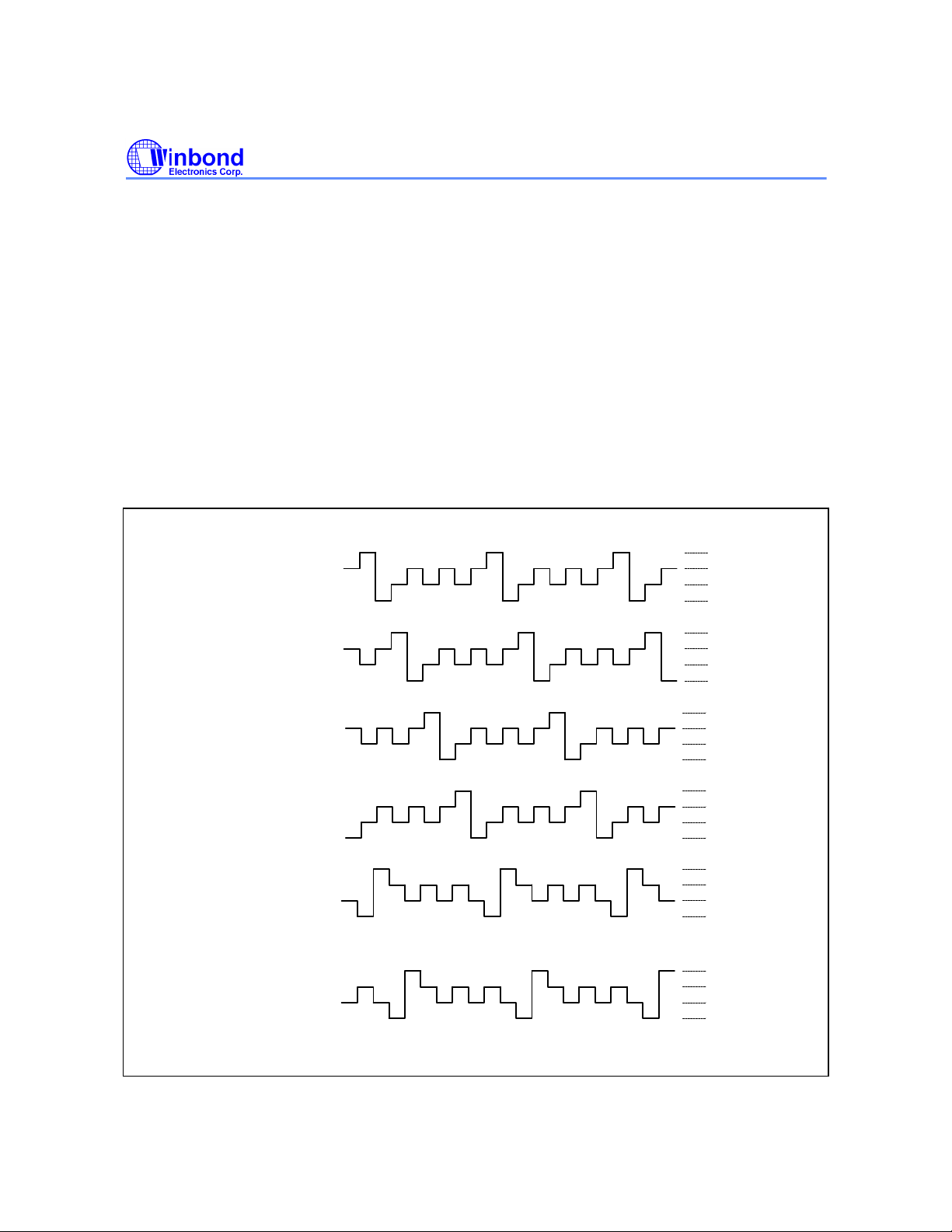
6.22.2 The output waveforms for the LCD driving mode
1/3 bias 1/4 duty Lighting System (Example)
Normal Operating Mode
COM0
COM1
COM2
COM3
LCD driver
outputs for
only seg. on
COM0 side
being lit
LCD driver
outputs for
only seg. on
COM1 side
being lit
VDD
VDD2
VDD1
VSS
VDD
VDD2
VDD1
VSS
VDD
VDD2
VDD1
VSS
VDD
VDD2
VDD1
VSS
VDD
VDD2
VDD1
VSS
VDD
VDD2
VDD1
VSS
Publication Release Date: May 1999
- 31 - Revision A1
Page 32
Continued
VDD = 3.0 V
LCD driver
outputs for
seg. on COM0,
COM1 sides
being lit
Preliminary W742C810
VDD2
VDD1
VSS
LCD driver
outputs for
seg. on COM1,
COM2,3 sides
being lit
LCD driver
outputs for
seg. on COM1
COM2 sides
being lit
LCD driver
outputs for
seg. on COM0
COM2,3 sides
being lit
LCD driver
outputs for
seg. on COM0
COM1,2,3 sides
being lit
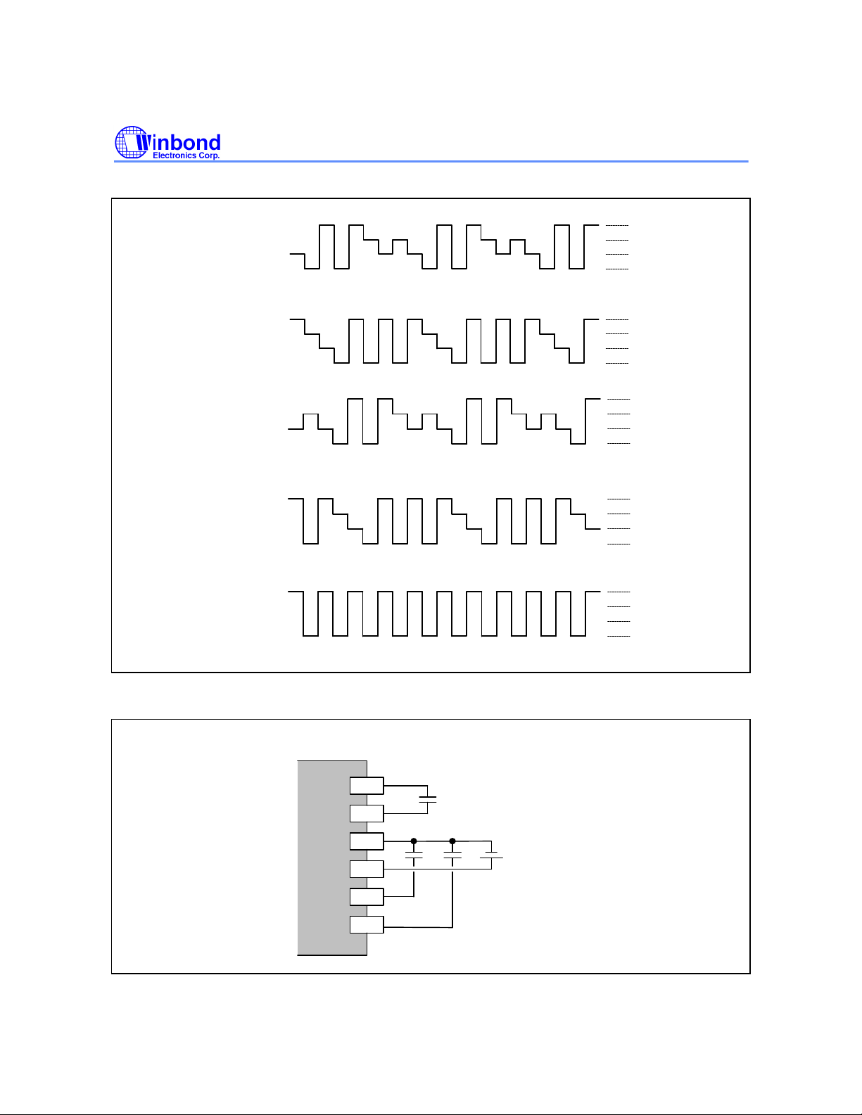
The power connections for the 1/3 bias 1/4 duty LCD driving mode are shown below.
VDD
VDD2
VDD1
VSS
VDD
VDD2
VDD1
VSS
VDD
VDD2
VDD1
VSS
VDD
VDD2
VDD1
VSS
1/3 Bias at VDD = 3.0 V
DH1
DH2
VSS
C
H
VDD
I
P
VDD1
VDD2
0.1uF
0.1uF
- 32 -
Page 33
Preliminary W742C810
7. ABSOLUTE MAXIMUM RATINGS
PARAMETER RATING UNIT
Supply Voltage to Ground Potential -0.3 to +7.0 V
Applied Input/Output Voltage -0.3 to +7.0 V
Power Dissipation 120 mW
Ambient Operating Temperature 0 to +70
Storage Temperature -55 to +150
Note: Exposure to conditions beyond those listed under Absolute Maximum Ratings may adversely affect the life and reliability
of the device.
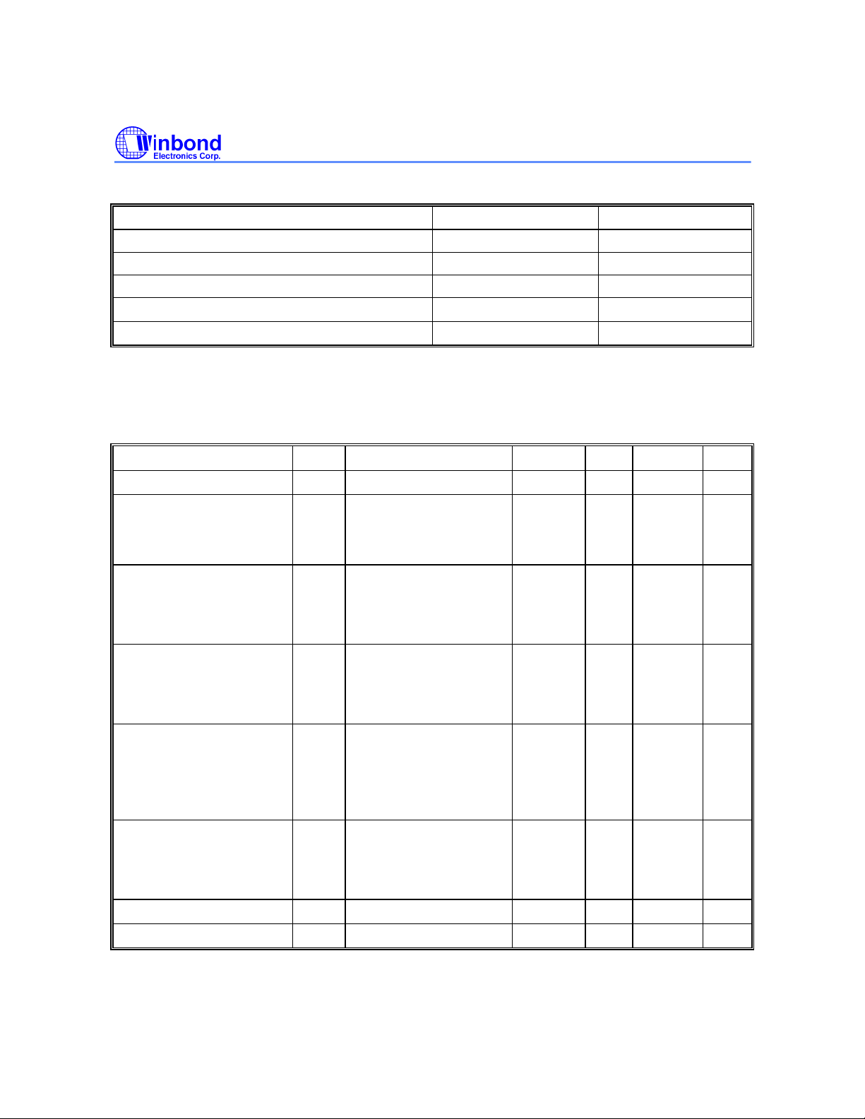
8. DC CHARACTERISTICS
(VDD-VSS = 3.0 V, Fm = 3.58 MHz, Fs = 32.768 KHz, TA = 25° C, LCD on; unless otherwise specified)
PARAMETER SYM. CONDITIONS MIN. TYP. MAX. UNIT
Op. Voltage VDD - 2.4 - 3.6 V
Op. Current (Crystal type) IOP1 No load (Ext-V)
In dual-clock normal
operation
- 0.7 1.0 mA
°C
°C
Op. Current (Crystal type) IOP3 No load (Ext-V)
In dual-clock slow
operation and when Fm
is stopped
Hold Current (Crystal
type)
Hold Current (Crystal
type)
Stop Current (Crystal
type)
Input Low Voltage VIL - VSS - 0.3 VDD V
Input High Voltage VIH - 0.7 VDD - VDD V
IHM1 Hold mode No load
(Ext-V)
In dual-clock normal
operation
IHM3 Hold mode No load
(Ext-V)
In dual-clock slow
operation and when Fm
is stopped
ISM1 Stop mode No load
(Ext-V)
In dual-clock normal
operation
- 20 30
- - 450
- 15 30
- - 6
µA
µA
µA
µA
Publication Release Date: May 1999
- 33 - Revision A1
Page 34
Preliminary W742C810
DC Characteristics, continued
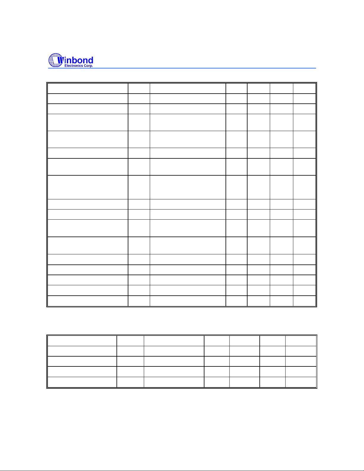
PARAMETER SYM. CONDITIONS MIN. TYP. MAX. UNIT
MFP Output Low Voltage VML IOL = 3.5 mA - - 0.4 V
MFP Output High Voltage VMH IOH = 3.5 mA 2.4 - - V
Port RA, RB, RD and RF
Output Low Voltage
Port RA, RB, RD and RF
Output high Voltage
LCD Supply Current ILCD All Seg. ON - - 6
SEG0-SEG39 Sink Current
(Used as LCD output)
SEG0-SEG39 Drive
Current
(Used as LCD output)
Port RE Sink Current IEL VOL = 0.9V 9 - - mA
Port RE Source Current IEH VOH = 2.4V 0.4 1.2 - mA
DTMF Output DC level VTDC
DTMF Distortion THD
DTMF Output Voltage VTO
Pre-emphasis Col/Row 1 2 3 dB
DTMF Output Sink Current ITL VTO = 0.5V 0.2 - - mA
Pull-up Resistor RC Port RC 100 350 1000
VABL IOL = 2.0 mA - - 0.4 V
VABH IOH = 2.0 mA 2.4 - - V
IOL1 VOL = 0.4V
VLCD = 0.0V
IOH1 VOH = 2.4V
VLCD = 3.0V
RL = 5KΩ,
VDD = 2.5 to 3.8V
RL = 5KΩ,
VDD = 2.5 to 3.8V
Low group, RL = 5KΩ
90 - -
90 - -
1.1 - 2.8 V
- -30 -23 dB
130 150 170 mVrms
µA
µA
µA
KΩ
RES Pull-up Resistor RRES - 20 100 500
9. AC CHARACTERISTICS
PARAMETER SYM. CONDITIONS MIN. TYP. MAX. UNIT
Op. Frequency FOSC Crystal type - 3.58 - MHz
Instruction cycle time TI One machine cycle - 4/FOSC - S
Reset Active Width TRAW FOSC = 32.768 KHz 1 - Interrupt Active Width TIAW FOSC = 32.768 KHz 1 - -
- 34 -
KΩ
µS
µS
Page 35

10. INSTRUCTION SET TABLE
Symbol Description
ACC: Accumulator
ACC.n: Accumulator bit n
WR: Working Register
WRP: WR Page register
PAGE: Page Register
DBKR: Data Bank Register
ROMPR: ROM Page Register
MR0: Mode Register 0
MR1: Mode Register 1
PM0: Port Mode 0
PM1: Port Mode 1
PM2: Port Mode 2
PM5: Port Mode 5
PSR0: Port Status Register 0
R: Memory (RAM) of address R
LP: LCD data RAM pointer
LPL: Low nibble of the LCD data RAM pointer
LPH: High nibble of the LCD data RAM pointer
R.n: Memory bit n of address R
I: Constant parameter
L: Branch or jump address
CF: Carry Flag
ZF: Zero Flag
PC: Program Counter
TM0L: Low nibble of the Timer 0 counter
TM0H: High nibble of the Timer 0 counter
TM1L: Low nibble of the Timer 1 counter
TM1H: High nibble of the Timer 1 counter
TAB0: Look-up table address buffer 0
TAB1: Look-up table address buffer 1
TAB2: Look-up table address buffer 2
TAB3: Look-up table address buffer 3
IEF.n: Interrupt Enable Flag n
Preliminary W742C810
Publication Release Date: May 1999
- 35 - Revision A1
Page 36
Preliminary W742C810
Instruction Set Table, continued
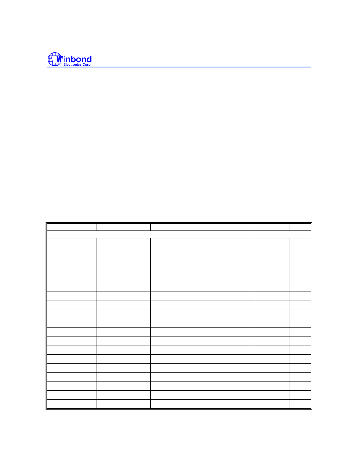
HCF.n: HOLD mode release Condition Flag n
HEF.n: HOLD mode release Enable Flag n
SEF.n: STOP mode wake-up Enable Flag n
PEF.n: Port Enable Flag n
EVF.n: Event Flag n
DTMF: DTMF Register
DTCR: DTMF Control Register
! =: Not equal
&: AND
^: OR
EX: Exclusive OR
←:
[PAGE*10H+()]: Contents of address PAGE(bit2, bit1, bit0)*10H+()
[P()]: Contents of port P
Transfer direction, result
Machine code Mnemonic Function Flag affected W/C
Arithmetic
0001 1000 0xxx xxxx ADD R, ACC
0001 1100 iiii nnnn ADD WRn, #I
0001 1001 0xxx xxxx ADDR R, ACC
0001 1101 iiii nnnn ADDR WRn, #I
0000 1000 0xxx xxxx ADC R, ACC
0000 1100 iiii nnnn ADC WRn, #I
0000 1001 0xxx xxxx ADCR R, ACC
0000 1101 iiii nnnn ADCR WRn, #I
0010 1000 0xxx xxxx ADU R, ACC
0010 1100 iiii nnnn ADU WRn, #I
0010 1001 0xxx xxxx ADUR R, ACC
0010 1101 iiii nnnn ADUR WRn, #I
0001 1010 0xxx xxxx SUB R, ACC
0001 1110 iiii nnnn SUB WRn, #I
0001 1011 0xxx xxxx SUBR R, ACC
0001 1111 iiii nnnn SUBR WRn, #I
0000 1010 0xxx xxxx SBC R, ACC
0000 1110 iiii nnnn SBC WRn, #I
0000 1011 0xxxxxxx SBCR R, ACC
ACC←(R) + (ACC)
ACC←(WRn) + I
ACC, R←(R) + (ACC)
ACC, WRn←(WRn) + I
ACC←(R) + (ACC) + (CF)
ACC←(WRn) + I + (CF)
ACC, R←(R) + (ACC) + (CF)
ACC, WRn←(WRn) + I + (CF)
ACC←(R) + (ACC)
ACC←(WRn) + I
ACC, R←(R) + (ACC)
ACC, WRn←(WRn) + I
ACC←(R) - (ACC)
ACC←(WRn) - I
ACC, R←(R) - (ACC)
ACC, WR←(WR) - I
ACC←(R) - (ACC) - (CF)
ACC←(WRn) - I - (CF)
ACC, R←(R) - (ACC) - (CF)
ZF, CF 1/1
ZF, CF 1/1
ZF, CF 1/1
ZF, CF 1/1
ZF, CF 1/1
ZF, CF 1/1
ZF, CF 1/1
ZF, CF 1/1
ZF 1/1
ZF 1/1
ZF 1/1
ZF 1/1
ZF, CF 1/1
ZF, CF 1/1
ZF, CF 1/1
ZF, CF 1/1
ZF, CF 1/1
ZF, CF 1/1
ZF, CF 1/1
- 36 -
Page 37
Preliminary W742C810
Instruction set, continued
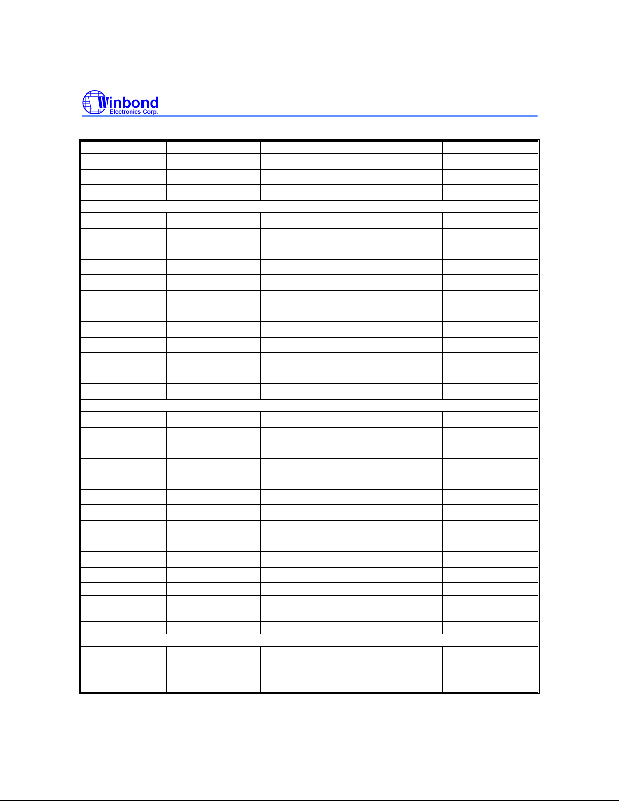
Machine code Mnemonic Function Flag affected W/C
0000 1111 iiii nnnn SBCR WRn, #I
0100 1010 0xxx xxxx INC R
0100 1010 1xxx xxxx DEC R
Logic
0010 1010 0xxx xxxx ANL R, ACC
0010 1110 iiii nnnn ANL WRn, #I
0010 1011 0xxx xxxx ANLR R, ACC
0010 1111 iiii nnnn ANLR WRn, #I
0011 1010 0xxx xxxx ORL R, ACC
0011 1110 iiii nnnn ORL WRn, #I
0011 1011 0xxx xxxx ORLR R, ACC
0011 1111 iiii nnnn ORLR WRn, #I
0011 1000 0xxx xxxx XRL R, ACC
0011 1100 iiii nnnn XRL WRn, #I
0011 1001 0xxx xxxx XRLR R, ACC
0011 1101 iiii nnnn XRLR WRn, #I
Branch
0111 0aaa aaaa aaaa JMP L
1000 0aaa aaaa aaaa JB0 L
1001 0aaa aaaa aaaa JB1 L
1010 0aaa aaaa aaaa JB2 L
1011 0aaa aaaa aaaa JB3 L
1110 0aaa aaaa aaaa JZ L
1100 0aaa aaaa aaaa JNZ L
1111 0aaa aaaa aaaa JC L
1101 0aaa aaaa aaaa JNC L
0100 1000 0xxx xxxx DSKZ R
0100 1000 1xxx xxxx DSKNZ R
1010 1000 0xxx xxxx SKB0 R
1010 1000 1xxx xxxx SKB1 R
1010 1001 0xxx xxxx SKB2 R
1010 1001 1xxx xxxx SKB3 R
Subroutine
0110 0aaa aaaa aaaa CALL L
0000 0001 0000 0000 RTN
ACC, WRn←(WRn) - I - (CF)
ACC, R←(R) + 1
ACC, R←(R) - 1
ACC←(R) & (ACC)
ACC←(WRn) & I
ACC, R←(R) & (ACC)
ACC, WRn←(WRn) & I
ACC←(R) ∧ (ACC)
ACC←(WRn) ∧ I
ACC, R←(R) ∧ (ACC)
ACC, WRn←(WRn) ∧ I
ACC←(R) EX (ACC)
ACC←(WRn) EX I
ACC, R←(R) EX (ACC)
ACC, WRn←(WRn) EX I
PC12~PC0←(ROMPR)×800H+L10~L0
PC10~PC0←L10~L0; if ACC.0 = "1"
PC10~PC0←L10~L0; if ACC.1 = "1"
PC10~PC0←L10~L0; if ACC.2 = "1"
PC10~PC0←L10~L0; if ACC.3 = "1"
PC10~PC0←L10~L0; if ACC = 0
PC10~PC0←L10~L0; if ACC ! = 0
PC10~PC0←L10~L0; if CF = "1"
PC10~PC0←L10~L0; if CF != "1"
ACC, R←(R) - 1; PC ← (PC) + 2 if ACC = 0
ACC, R←(R) - 1; PC ← (PC) + 2 if ACC != 0
PC ← (PC) + 2 if R.0 = "1"
PC ← (PC) + 2 if R.1 = "1"
PC ← (PC) + 2 if R.2 = "1"
PC ← (PC) + 2 if R.3 = "1"
STACK ← (PC)+1;
PC12 ~ PC0 ← (ROMPR)×800H+L10 ~ L0
(PC)← STACK
ZF, CF 1/1
ZF, CF 1/1
ZF, CF 1/1
ZF 1/1
ZF 1/1
ZF 1/1
ZF 1/1
ZF 1/1
ZF 1/1
ZF 1/1
ZF 1/1
ZF 1/1
ZF 1/1
ZF 1/1
ZF 1/1
ZF, CF 1/1
ZF, CF 1/1
1/1
1/1
1/1
1/1
1/1
1/1
1/1
1/1
1/1
1/1
1/1
1/1
1/1
1/1
1/1
Publication Release Date: May 1999
- 37 - Revision A1
Page 38
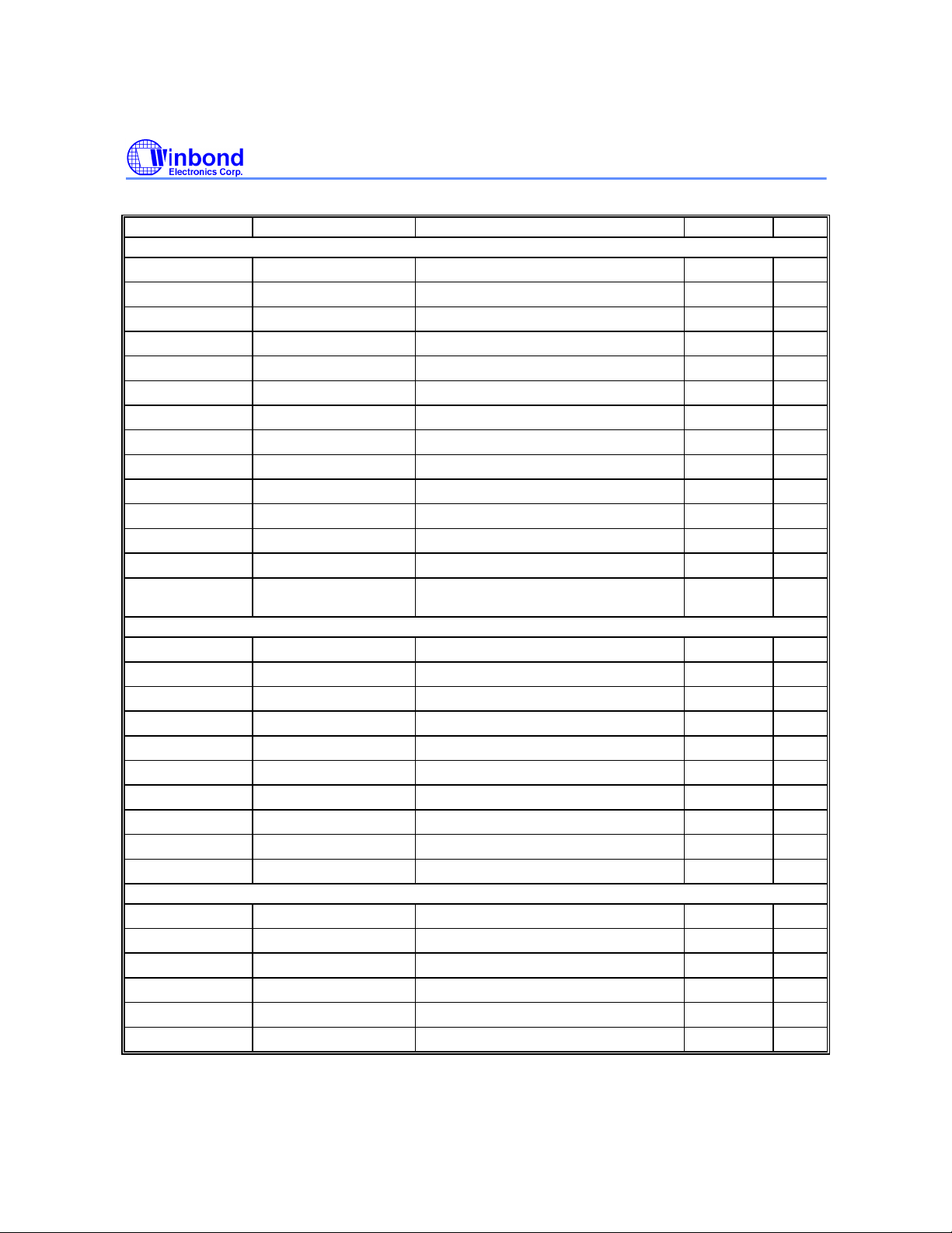
Preliminary W742C810
Instruction set, continued
Machine code Mnemonic Function Flag affected W/C
Data move
1110 1nnn nxxx xxxx MOV WRn, R
1111 1nnn nxxx xxxx MOV R, WRn
0110 1nnn nxxx xxxx MOVA WRn, R
0111 1nnn nxxx xxxx MOVA R, WRn
0101 1001 1xxx xxxx MOV R, ACC
0100 1110 1xxx xxxx MOV ACC, R
1011 1 iii ixxx xxxx MOV R, #I
1100 1nnn n000 qqqq MOV WRn, @WRq
1101 1nnn n000 qqqq MOV @WRq, WRn
1000 1100 0xxx xxxx MOV TAB0, R
1000 1100 1xxx xxxx MOV TAB1, R
1000 1110 0xxx xxxx MOV TAB2, R
1000 1110 1xxx xxxx MOV TAB3, R
1000 1101 0xxx xxxx MOVC R
Input & Output
0101 1011 0xxx xxxx MOVA R, RA
0101 1011 1xxx xxxx MOVA R, RB
0100 1011 0xxx xxxx MOVA R, RC
0100 1011 1xxx xxxx MOVA R, RD
0101 1010 0xxx xxxx MOV RA, R
0101 1010 1xxx xxxx MOV RB, R
1010 1100 1xxx xxxx MOV RD, R
0101 1110 0xxx xxxx MOV RE, R
1010 1110 0xxx xxxx MOV RF, R
0001 0010 iiii iiii MOV MFP, #I
Flag & Register
0101 1111 1xxx xxxx MOVA R, PAGE
0101 1110 1xxx xxxx MOV PAGE, R
0101 0110 1000 0iii MOV PAGE, #I
1001 1101 1xxx xxxx MOV R, WRP
1001 1100 1xxx xxxx MOV WRP, R
0011 0101 1000 iiii MOV WRP, #I
WRn←(R)
R←(WRn)
ACC, WRn←(R)
ACC, R←(WRn)
R←(ACC)
ACC←(R)
R←I
WRn←[(DBKR)×80H+(PAGE)x10H +(WRq)]
[(DBKR)×80H+(PAGE)x10H +(WRq)]←WRn
TAB0←(R)
TAB1←(R)
TAB2←(R)
TAB3←(R)
R←[(TAB3)×1000H+(TAB2)×100H+(TAB1)
x10H + (TAB0)]
ACC, R←[RA]
ACC, R←[RB]
ACC, R←[RC]
ACC, R←[RD]
[RA]←(R)
[RB]←(R)
[RD]←(R)
[RE]←(R)
[RF]←(R)
[MFP]← I
ACC, R←PAGE (Page Register)
PAGE←(R)
PAGE←I
R←WRP
WRP←(R)
WRP←I
ZF 1/1
ZF 1/1
ZF 1/1
ZF 1/1
ZF 1/1
ZF 1/1
ZF 1/1
ZF 1/1
1/1
1/1
1/1
1/1
1/2
1/2
1/1
1/1
1/1
1/1
1/2
1/1
1/1
1/1
1/1
1/1
1/1
1/1
1/1
1/1
1/1
1/1
- 38 -
Page 39
Preliminary W742C810
Instruction set, continued
Machine code Mnemonic Function Flag affected W/C
1001 1101 0000nnnn MOV WRn,DBKR
1001 1100 0000nnnn MOV DBKR, WRn
0011 0101 0000 0iii MOV DBKR, #I
0011 0100 0000 00ii MOV ROMPR, #I
1000 1000 0xxx xxxx MOV ROMPR, R
1000 1001 0xxx xxxx MOV R, ROMPR
0001 0011 1000 i00i MOV MR0, #I
0001 0011 0000 iiii MOV MR1, #I
0101 1001 0xxx xxxx MOVA R, CF
0101 1000 0xxx xxxx MOV CF, R
0100 1001 0xxx xxxx MOVA R, HCFL
0100 1001 1xxx xxxx MOVA R, HCFH
0101 0011 0000 iiii MOV PM0, #I
0101 0111 0000 iiii MOV PM1, #I
0101 0111 1000 iiii MOV PM2, #I
0011 0111 1000 iiii MOV PM5, #I
0100 0000 i00i0iii CLR EVF, #I Clear Event Flag if In = 1 1/1
0100 0001 i00i0iii MOV HEF, #I Set/Reset HOLD mode release Enable Flag 1/1
0101 0001 i00i0iii MOV IEF, #I Set/Reset Interrupt Enable Flag 1/1
0100 0011 0000 iiii MOV PEF, #I Set/Reset Port Enable Flag 1/1
0101 0010 0000 iiii MOV SEF, #I Set/Reset STOP mode wake-up Enable Flag
0101 0100 0000 iiii MOV SCR, #I
0100 1111 0xxx xxxx MOVA R, PSR0
0100 0010 0000 0000 CLR PSR0 Clear Port Status Register 0 1/1
0101 0000 0100 0000 SET CF Set Carry Flag CF 1/1
0101 0000 0000 0000 CLR CF Clear Carry Flag CF 1/1
0001 0111 0000 0000 CLR DIVR0 Clear the last 4-bit of the Divider 0 1/1
0101 0101 1000 0000 CLR DIVR1 Clear the last 4-bit of the Divider 1 1/1
0001 0111 1000 0000 CLR WDT Clear WatchDog Timer 1/1
Shift & Rotate
0100 1101 0xxx xxxx SHRC R
WRn←DBKR
DBKR←WRn
DBKR←I
ROMPR←I
ROMPR←(R)
R←(ROMPR)
MR0←I
MR1←I
ACC.0, R.0←CF
CF←(R.0)
ACC, R←HCF.0~HCF.3
ACC, R←HCF.4~HCF.7
Port Mode 0← I
Port Mode 1← I
Port Mode 2← I
Port Mode 5← I
for RC port
SCR←I
ACC, R←Port Status Register 0
ACC.n, R.n←(R.n+1);
ACC.3, R.3←0; CF←R.0
ZF 1/1
CF 1/1
ZF 1/1
ZF 1/1
ZF 1/1
ZF, CF 1/1
1/1
1/1
1/1
1/1
1/1
1/1
1/1
1/1
1/1
1/1
1/1
1/1
1/1
1/1
Publication Release Date: May 1999
- 39 - Revision A1
Page 40
Preliminary W742C810
Instruction set, continued
Machine code Mnemonic Function Flag affected W/C
0100 1101 1xxx xxxx
0100 1100 0xxx xxxx
0100 1100 1xxx xxxx
LCD
1001 1000 0xxx xxxx
1001 1000 1xxx xxxx
1001 1010 0xxx xxxx
1001 1011 0xxx xxxx
0000 0010 0000 0000
0000 0010 1000 0000
DTMF
1001 1110 1xxx xxxx
0011 0100 1000 0 i i i
Timer
1010 1010 0xxx xxxx
1010 1010 1xxx xxxx
1010 1011 0xxx xxxx
1010 1011 1xxx xxxx
Other
0000 0000 1000 0000
0000 0000 1100 0000
0000 0000 0000 0000
0101 0000 1100 0000
0101 0000 1000 0000
RRC R
SHLC R
RLC R
MOV LPL, R
MOV LPH, R
MOV @LP, R
MOV R, @LP
LCDON LCD ON 1/1
LCDOFF LCD OFF 1/1
MOV DTMF, R
MOV DTCR, #I
MOV TM0L, R
MOV TM0H, R
MOV TM1L, R
MOV TM1H, R
HOLD Enter Hold mode 1/1
STOP Enter Stop mode 1/1
NOP No operation 1/1
EN INT Enable interrupt function 1/1
DIS INT Disable interrupt function 1/1
ACC.n, R.n←(R.n+1);
ACC.3, R.3←CF; CF←R.0
ACC.n, R.n←(R.n-1);
ACC.0, R.0←0; CF←R.3
ACC.n, R.n←(R.n-1);
ACC.0, R.0←CF; CF←R.3
LPL←(R)
LPH←(R)
[(LPH)×10H+(LPL)]←(R)
R←[(LPH) ×10H+(LPL)]
DTMF←(R)
DTCR← I
TM0L←(R)
TM0H←(R)
TM1L←(R)
TM1H←(R)
ZF, CF 1/1
ZF, CF 1/1
ZF, CF 1/1
1/1
1/1
1/1
1/1
1/1
1/1
1/1
1/1
1/1
1/1
- 40 -
Page 41
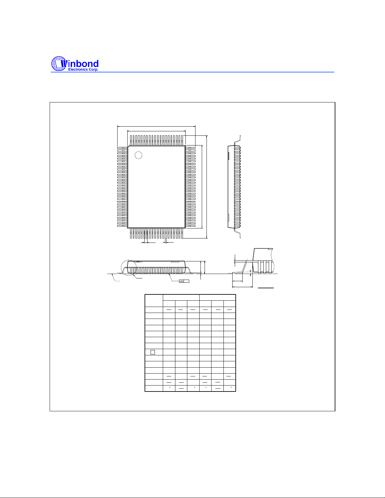
11. PACKAGE DIMENSIONS
100-pin QFP
Preliminary W742C810
H
D
D
E
H
E
Seating Plane
e b
See Detail F
y
Controlling dimension: Millimeters
Dimension in inches
Symbol
Min.
Nom.
Max. Max.
A
A
1
0.101
2
A
0.008
b
0.004
c
0.547
D
0.783
E
0.020 0.032
e
0.746
D
H
0.960
E
H
0.039
L
1
L
y
0.113
0.107
0.016
0.012
0.006 0.15
0.008
0.555
0.551
0.791
0.787
0.026
0.756
0.740
0.992
0.976
0.055
0.047
0.064
0.003
θ
AA2
A1
Dimension in mm
Min.
2.57
0.20
0.10
13.90
19.90
0.498
18.40
24.40
1.00
070
Nom.
0.350.250.010 0.014 0.018 0.45
2.87
2.72
0.40
0.30
0.20
14.00
14.10
20.00
20.10
0.65
0.802
19.20
18.80
24.80 25.20
1.40
1.20
2.40
0.08
7
c
θ
L
L
1
Publication Release Date: May 1999
- 41 - Revision A1
Page 42

Preliminary W742C810
Headquarters
No. 4, Creation Rd. III,
Science-Based Industrial Park,
Hsinchu, Taiwan
TEL: 886-3-5770066
FAX: 886-3-5792766
http://www.winbond.com.tw/
Voice & Fax-on-demand: 886-2-27197006
Winbond Electronics (H.K.) Ltd.
Rm. 803, World Trade Square, Tower II,
123 Hoi Bun Rd., Kwun Tong,
Kowloon, Hong Kong
TEL: 852-27513100
FAX: 852-27552064
Taipei Office
11F, No. 115, Sec. 3, Min-Sheng East Rd.,
Taipei, Taiwan
TEL: 886-2-27190505
FAX: 886-2-27197502
Note: All data and specifications are subject to change without notice.
- 42 -
Winbond Electronics North America Corp.
Winbond Memory Lab.
Winbond Microelectronics Corp.
Winbond Systems Lab.
2727 N. First Street, San Jose,
CA 95134, U.S.A.
TEL: 408-9436666
FAX: 408-5441798
 Loading...