

Page 1

Preliminary W6662CF
SCANNER ANALOG FRONT END
Publication Release Date: December 1998
- 1 - Revision A1
1. GENERAL DESCRIPTION
The W6662 is a highly integrated CCD/CIS analog front end signal processor. It provides the
components required for all necessary front-end signal process of a CCD/CIS scanner, including a 3channel input clamp circuit for correlated double sampling (short as CDS) mode, a multiplexer to mux
3-channel inputs to a correlated double sampling (CDS) circuit, a programmable offset adjusted and
gain controlled amplifier, a 12-bit analog-to-digital converter.
CDS or S&H (sample and hold) of operation modes can be chosen. The device configuration is
programmed via 3-wire or 4-wired interface, operation modes, offset and gain value of each channel
can be programmed.
2. FEATURES
• 12-bit A/D Converter
• No Missing Code Guaranteed
• Three channels analog input with clamp circuit individually
• Integrated Correlated Double Sampler (CDS)
• Supports Contact Image Sensors (CIS)
• Accept CCD/CIS sensor with three channel or single channel analog out
• External offset voltage input for CIS reference voltage
• Built-in bandgap reference circuit for CDS mode and A/D Converter
• Integrated 6-bit Programmable Gain Amplifier (PGA) with 3-channel register selected
• Integrated 8-bit offset adjustment with 3-channel register selected
• 3 MHz sampling rate of offset/gain adjustment circuit
• Three-wired or four-wired Serial Interface programmable
• Registers readback capability
• Low power CMOS device
• Power down mode supported
• 3/5V digital I/O pin
• Packageed in 48-pin QFP
Applications:
Flatbed Scanners
Sheetfeed Scanners
Film Scanners
Page 2
Preliminary W6662CF
- 2 -
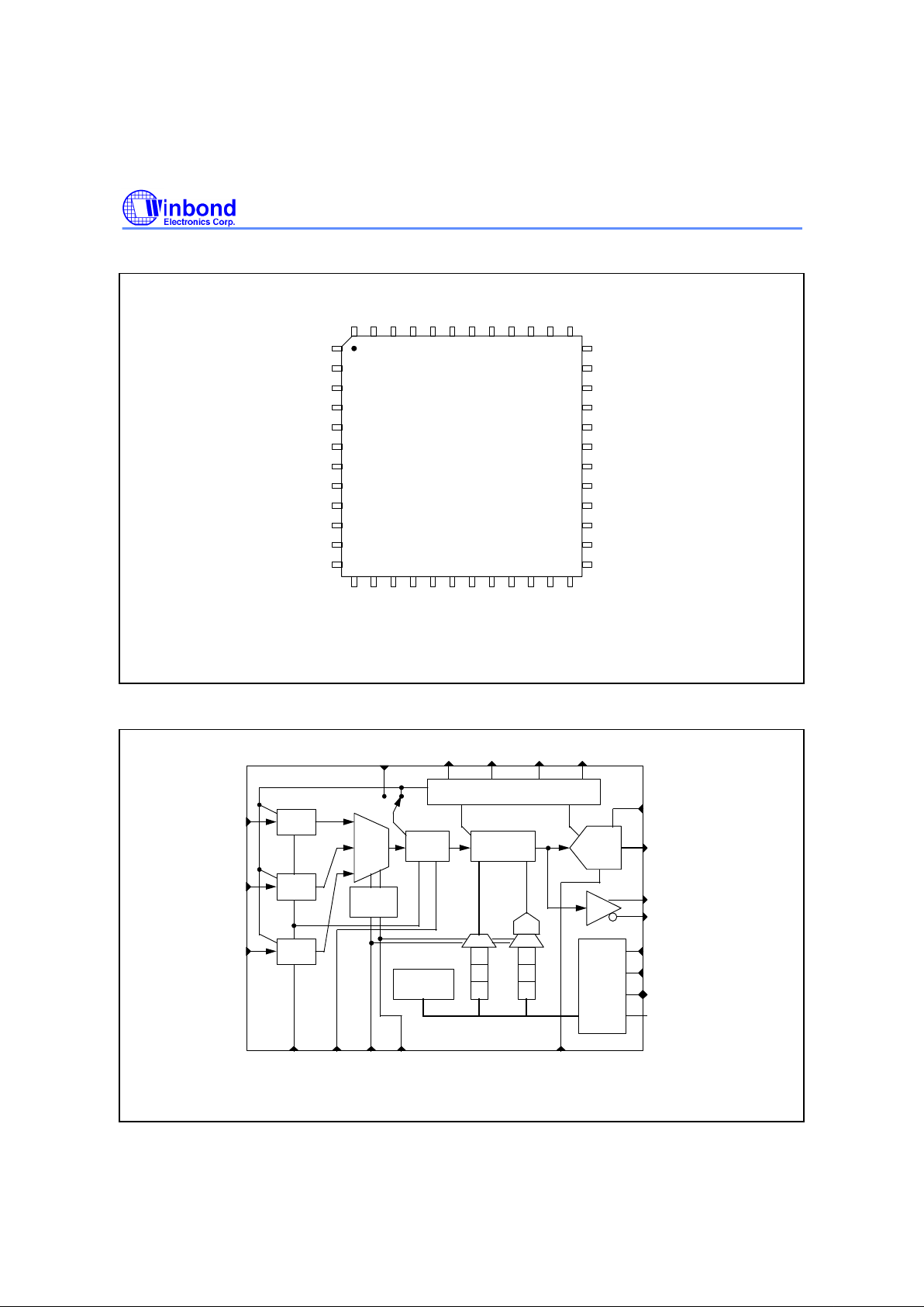
3. PIN CONFIGURATION
Fig. 3-1 Pin Assignments.
PAOUT
PAOUTN
AVDD
AVSS
VRDT
VRDT
VRDB
VRDB
VREF
VRDC
VINR
AVSS
VING
AVSS
VINB
AVSS
CISREF
CDSCK1
ADCCLK
CDSCK2
DRVSS
DRVDD
AVDD
SEL0
SCLK
SDI/SDIO
SDO/SMS
SEN
DOUT0
DOUT1
DOUT2
DOUT3
DOUT4
AVSS
AVDD
DOUT6
DOUT7
DOUT8
DOUT9
DOUT10
DOUT11
OEN
1
2
3
4
5
6
7
8
9
10
11
12
13 14 15 16 17 18 19 20 21 22 23 24
25
26
27
28
29
30
31
32
33
34
35
36
3738394041424344
DOUT5
SEL1
NC
NC
NC
NC
45464748
W6662CF
Winbond
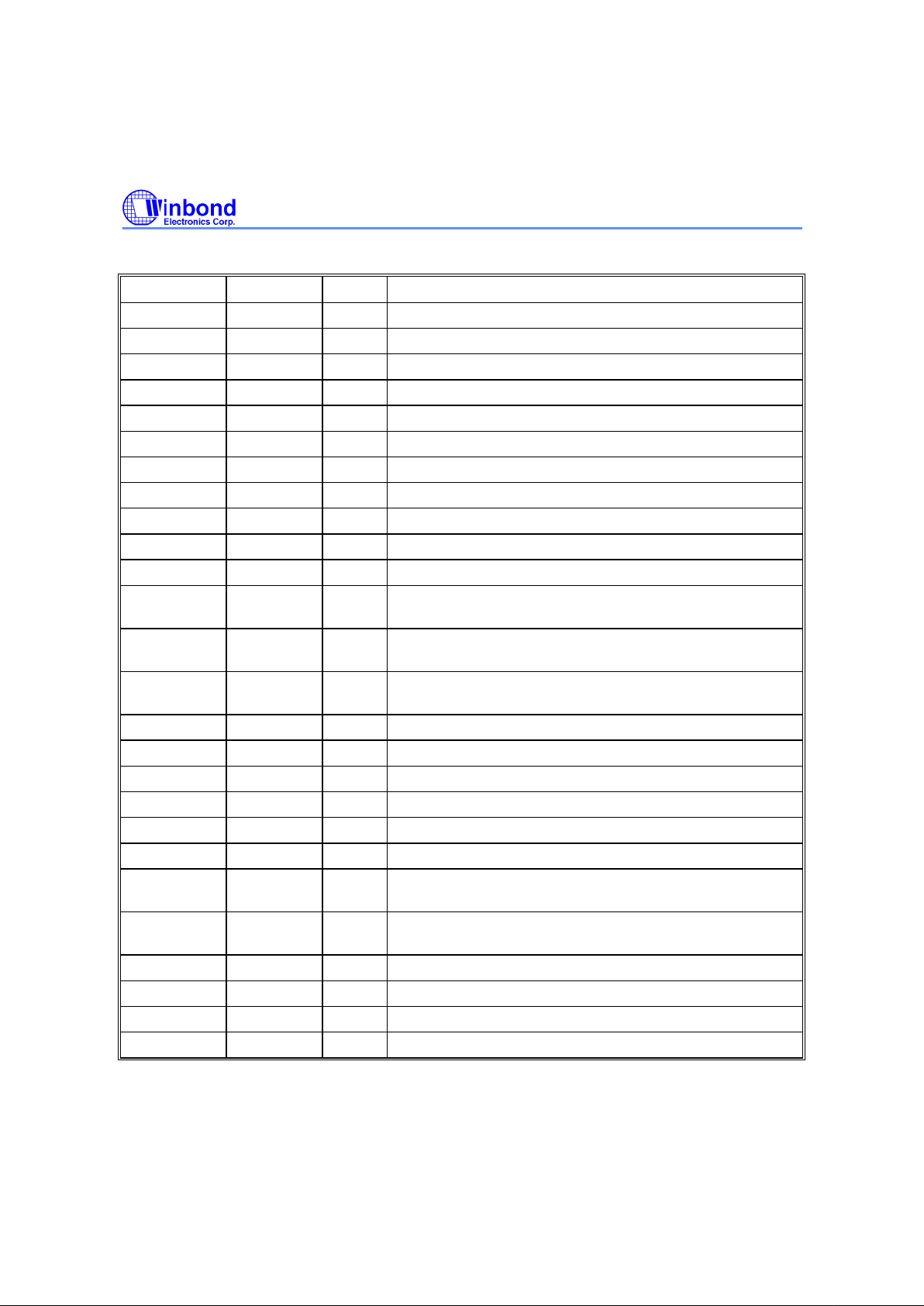
4. BLOCK DIAGRAM
Fig. 4 The Block Diagram of W6662 Device.
Clamp
MUX
12-bit
ADC
Serial
I/O port
control
Bandgap Reference Circuit
Clamp
Gain/Offset
Adjust
Clamp
VINR
VING
VINB
CDSCK1 CDSCK2
DOUT[11:0]
SCLK
SEN
SDI/SDIO
DAC
Offset
Registers
Gain
Registers
Configuration
Register
CISREF
PAOUT
PAOUTN
R
G
B
OEN
ADCCLK
R
G
B
MUX MUX
SEL0 SEL1
CDS
Process
I/P MUX
Ctrl
SDO/SMS
Weak
Drive
CDS
VREF VRDC VRDB VRDT
Page 3
Preliminary W6662CF
Publication Release Date: December 1998
- 3 - Revision A1
5. PIN DESCRIPTIONS
PIN NAME TYPE DESCRIPTION
10, 37, 44 AVDD AP Analog Power Supply.
4, 6, 8, 35, 42 AVSS AP Analog Ground.
45, 46 VRDT AO Voltage Reference Decoupling (Top).
47, 48 VRDB AO Voltage Reference Decoupling (Bottom).
1 VRDC AO Voltage Reference Decoupling (Center).
2 VREF AO Internal Reference Output.
3 VINR AI Analog Input, Red Channel.
5 VING AI Analog Input, Green Channel.
7 VINB AI Analog Input, Blue Channel.
11 CISREF AI Reference Voltage Input when CIS input.
12 PAOUT AO PGA Output, low speed analog monitor output for test only.
13 PAOUTN AO PGA Output (negative), low speed analog monitor output for
test only.
14 CDSCK1 DI CDS Clock 1 (Schmitt Trigger Input), Reset Level Sampling
Clock.
15 CDSCK2 DI CDS Clock 2 (Schmitt Trigger Input), Data Level Sampling
Clock.
16 ADCCLK DI A/D Converter Sampling Clock (Schmitt Trigger Input).
19 DRVDD DP Digital Driver Power Supply.
17 DRVSS DP Digital Driver Ground.
20 SEL0 DI Channel Select bit 0.
21 SEL1 DI Channel Select bit 1.
22 SCLK DI Clock Input of Serial Interface (Schmitt Trigger Input).
23 SDI/SDIO DI/DO Serial Interface of Data Input or Serial Interface of Data
Input/Output.
24 SDO/SMS DI, DO Serial Interface of Data Output, Serial Interface Mode
Select.
25 SEN DI Enable Signal of Serial Interface, Active Low.
26:34 DOUT[0:8] DO Data Output Bit, DOUT0 is LSB.
38:40 DOUT[9:11] DO Data Output Bit, DOUT11 is MSB.
41 OEN DI Output Enable, Active Low.
Type: AP is Analog Power, AI is Analog Input, AO is Analog Output, DP is Digital Power, DI is Digital Input, DO is Digital
Output.
Page 4

Preliminary W6662CF
- 4 -
6. FUNCTIONAL DESCRIPTIONS
Figure 4 is the block diagram of W6662, it consists of three channel clamp circuit for CDS mode, a
multiplexer to mux 3-channel inputs and outputs to a correlated double sampling (CDS), a
programmable gain control and offset adjustment amplifier, a 12-bit analog-to-digital converter.
Bandgap reference circuit generate voltage reference signals for input signals clampping and
correlated sampling use (in CDS mode), for offset D/A converter and output A/D converter use. The
select signals SEL1 and SEL0 are used to select the offset registers and gain registers, the input
channels may be selected simultaneously.
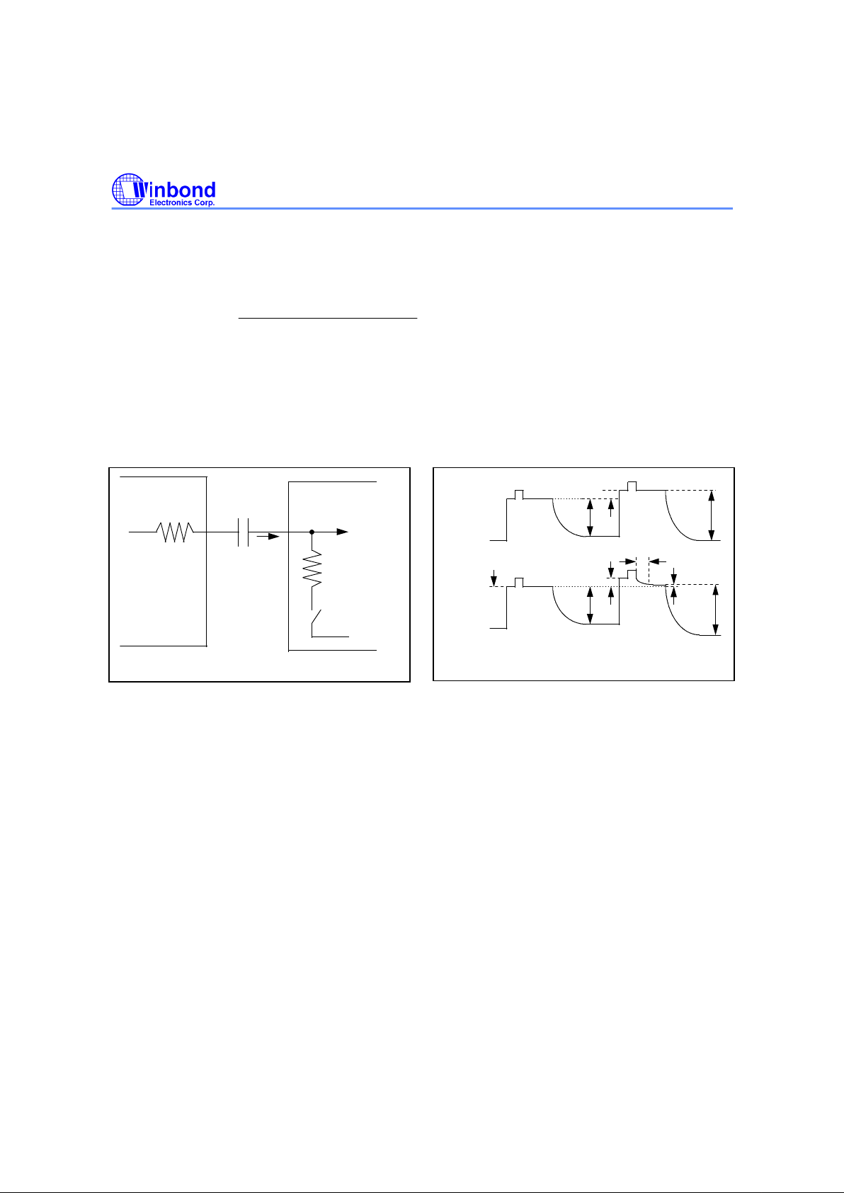
6.1 Clamp Circuit
The capacitor between the output of CCD/CIS device and W6662 is used to block the DC voltage
(even as high voltage). The clamp circuit is used to remove unwanted common-mode voltage in the
input pixel data and to get a maximum input signal span when the input is driven by CCD device as
shown in Figure 6-1. The input pins of W6662 are clampped to a internal offset voltage while valid
pixel signal is input. The clamp switches at three channels of figure 6-1 are turn on whenever
CDSCK1 goes high. Figure 6-2 shows the waveform between output of CCD device and input of
W6662, the voltage change on the capacitor will be clampped.
The value of input capacitor is calculated as follows:
tCLP
CMAX =
(RON + RCCDS) × ln (VC/VCLPTolerance)
IBIAS × tC2I
CMIN =
dV
where
CMAX is the maximum capacitor value.
CMIN is the minimum capacitor value.
tCLP is the high pulse width of the CDSCK1 clock input.
RON is switch resistance during clampping and is equivalent to 5K.
RCCDS is the source resistance of CCD device.
VC is the voltage change on the input capacitor must be clampped.
VCLPTolerance is the tolerance voltage error at the end of clampping.
IBIAS is the input leakage current on the input of the W6662 device.
dV is the maximum voltage drift on the input of the W6662 device.
tC2I is the time stamp from the end of clampping point to the acture input data sampling point, equal
to tC2S + tSPD + tACD or may be approximated as conversion time tCVR.
Page 5
Preliminary W6662CF
Publication Release Date: December 1998
- 5 - Revision A1
If input capacitor value is specified as CIN, the following is the equation to calculate how many lines
are required before the capacitor settles to the desired accuracy after power is up:
(RON + RCCDS) × CIN
LN = ln (VOFS/VCLPTolerance )
PIXN × tCLP
where
LN is line number.
PIXN is the total pixel number in one line.
CIN is the input capacitor value, 0.01 µF is suggestion value.
VOFS is the internal offset voltage to be clampped on the input terminal of the input capacitor.
Fig. 6-1 Equivalent Circuit of Clampping.
R
ON
= 5K
R
CCDS
C
IN
Input to MUX
V
OFS
W6662
CCD Device
I
BIAS
on when
CDSCK1= high
0.01uF
Fig. 6-2 CCD Input Clamp Waveform.
Output
signal
from CCD
Input
signal
to W6662
V
C
(Pixel n)
(Pixel n+1)
t
CLP
V
CLPTolerance
V
C
V
DATAn
V
DATAn
V
DATAn+1
V
DATAn+1
V
OFS
6.2 MUX and Channel Select
The analog input signal may be three channels or single channel and is specified in configuration
register. Three channel input or single channel input are described as follows:
The three channel input is used for red, green and blue analog signal input, selected by SEL1 and
SEL0 signals. The channel select signals SEL1 and SEL0 may be 01, 10, 11 and listed as follows:
SEL1 = 0, SEL0 = 1 is red channel input selected, red channel of gain register and offset register also
selected.
SEL1 = 1, SEL0 = 0 is green channel input selected, green channel of gain register and offset register
also selected.
SEL1 = 1, SEL0 = 1 is blue channel input selected, blue channel of gain register and offset register
also selected.
SEL1 = 0, SEL0 = 0 is reserved.
The one channel input is used for black and white CCD/CIS sensor or multiplexed color CCD/CIS
sensor output. Any channel input of red, green or blue can be used, other un-used analog input must
tight to VSS in S & H mode. The channel select signals SEL1 and SEL0 is used to select offset
register and gain register only and may be 01, 10, 11, described as follows:
Page 6
Preliminary W6662CF
- 6 -
SEL1 = 0, SEL0 = 1 is red channel of gain register and offset register selected.
SEL1 = 1, SEL0 = 0 is green channel of gain register and offset register selected.
SEL1 = 1, SEL0 = 1 is blue channel of gain register and offset register selected.
SEL1 = 0, SEL0 = 0 is reserved.
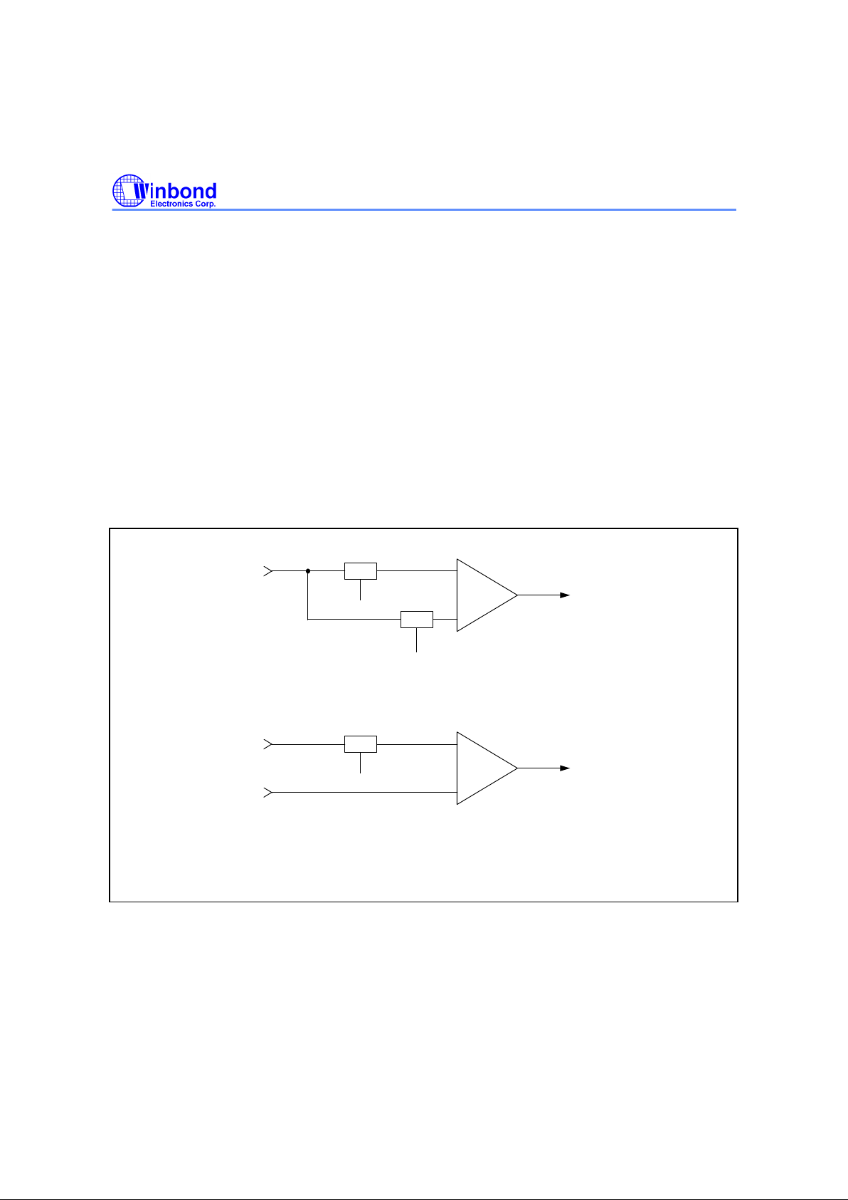
6.3 CDS vs S&H Mode
"CDS" stands for "correlated double sampling". It is used to reduce noise generated in CCD source
and to decrease the sampling error which induced from clampping voltage error. CDS takes two step
to sample a CCD's output pixel. In the first step, the reset level of CCD output is sampled and hold by
S/H1 at the falling edge of CDSCK1 signal. In the second step, the data signal of CCD output is
sampled and hold by S/H2 at the falling edge of CDSCK2 signal. The CDS output voltage is obtained
from the voltage difference of the outputs of S/H1 and S/H2.
In S&H mode, the data signal of CIS output is sampled and hold by S/H1 at the falling edge of
CDSCK2 signal and the output voltage is obtained from the voltage difference of the outputs of S/H1
and CISREF pin. Figure 6-3 shows the equivalent circuits of CDS and S&H mode processing.
Fig. 6-3 The Equivalent Circuit of CDS and S&H Mode.
S/H1
S/H2
CDSCK1
CDSCK2
+
-
From
I/P
MUX
To
Gain/Offset
Adjust
S/H1
CDSCK2
+
-
From
I/P
MUX
To
Gain/Offset
Adjust
(a) CDS Mode.
(b) S&H Mode.
From
CISREF
pin
6.4 Gain/Offset Adjustment
The analog input signal after CDS or S&H processed is amplified by PGA gain adjustment and then
shifted by offset value. The offset value will not affected by the PGA gain adjustment.
Page 7

Preliminary W6662CF
Publication Release Date: December 1998
- 7 - Revision A1
PGA Gain Adjustment
"PGA" stands for "programmable gain amplifier", it can provide analog gain for "not enough level for
A/D converter" input signals. The gain value is converted from PGA_code of gain register and is
selected by channel select SEL1 and SEL0. The gain formula is:
PGA_code
analog gain = 1 +
12
PGA_code = 0−63 and the gain = 1−6.25.
Offset Adjustment
The analog signal level can be shifted by offset level and to get maximum linear region. The offset
level is converted from offset value by internal D/A converter and the offset value is selected by
channel select SEL1 and SEL0.
The mapping between offset register code and offset value is as follows:
OFFSET REGISTER OFFSET VALUE
1111 1111 (LSB) +200 mV
: :
: :
1000 0001 +1.6 mV
1000 0000 0.0 mV
0000 0000 0.0 mV
0000 0001 -1.6 mV
: :
: :
0111 1111 -200 mV
6.5 Analog Monitor
The analog differential signal of PAOUT and PAOUTN is used to monitor the output waveform after
gain and offset adjustment process. The CCD or CIS pixel rate must operate below or equal 1MHz
and at most one probe loading on the PAOUT and PAOUTN to get a correct voltage output. In normal
operation, the PAOUT and PAOUTN must be turned off by writting a specified bit on the configuration
register to avoid the interference of noise and extra capacitance loading.
6.6 Internal Registers
The registers in the W6662 is configuration register, three channel offset registers and three channel
gain registers, these registers are addressed by A2, A1 and A0. The registers can be read or modified
through 3-wired or four-wired serial interface. During address phase, if SDO/SMS pin is low, threewired is selected, the three-wired interface are SEN, SCLK and SDIO signals, if SDO/SMS pin is
high, four-wired interface is selected, the four-wired interface are SEN, SCLK SDI and SDO signals.
Figure 6-4 shows the setting of the serial interface. For three-wired interface setting, the SDO/SMS
pin must connected to VSS. For four-wired interface, it only need to connect a pull high resistor on the
SDO/SMS pin. The signal format on the serial interface is listed as follows:
Page 8

Preliminary W6662CF
- 8 -
R/W A0 A1 A2 -- -- -- -- D0 D1 D2 D3 D4 D5 D6 D7
Address phase Data phase
R/W is read (high) or write (low) command to access the register.
A0, A1 and A2 is the address select bits of the register.
D0 throuth D7 is the data bit of the register, D7 is MSB and D0 is LSB.
The address of the registers is:
A2 A1 A0 REGISTER
0 0 0 Configuration Register
0 0 1 Red PGA Register
0 1 0 Green PGA Register
0 1 1 Blue PGA Register
1 0 0 Red Offset Register
1 0 1 Green Offset Register
1 1 0 Blue Offset Register
1 1 1 Reserved
Configuration Register
The bit definition of configuration register is:
A. Configuration mode (wake up and configuration)
bit 0 = 0: 1.5V input span.
1: 3.0V input span.
bit 1 = 0: S&H mode.
1: CDS mode.
bit [3:2] = 0 0: Red channel input only.
0 1: Green channel input only.
1 0: Blue channel input only.
1 1: Three channels input and selected by SEL1 and SEL0 signals.
bit 4 = Reserved (must set to 0).
bit 5 = 0: PAOUT and PAOUTN enable.
1: PAOUT and PAOUTN disable.
bit 6 = Reserved (must set to 0).
bit 7 = 0.
Page 9

Preliminary W6662CF
Publication Release Date: December 1998
- 9 - Revision A1
B. Power down mode
bit [6:0] = don't care.
bit 7 = 1.
The CDSCK1, CDSCK2, ADCCLK and SCLK must hold at stable state after power down mode has
been configured to ensure the W6662 is in low power state. The system must wait at least 10 mS to
ensure that the device is power up completedly if the configuration register is programmed with bit 7
= 0.
PGA Registers
The mapping of PGA registers and PGA_code is:
bit [5:0] PGA_code, bit 5 is MSB, bit 0 is LSB.
bit [7:6] reserved (must set to 0).
The offset registers are described in PGA gain/offset adjustment section.
Fig. 6-4 Configuration Serial Interface Modes.
(a). Three-wired Interface Mode Selected.
(b). Four-wired Interface Mode Selected.
W6662
SCLK
SEN
SDIO
SMS
Micro-controller
or
System Controller
or
Core Chip
May drive another peripherals
chip select
W6662
SCLK
SEN
SDI
SDO
May drive another peripherals
chip select
Micro-controller
or
System Controller
or
Core Chip
DRVDD
Page 10

Preliminary W6662CF
- 10 -
7. ELECTRICAL CHARACTERISTICS
7.1 Maximum Ratings*
PARAMETER SYMBOL RATING UNITS
Supply Voltage with respect to AVSS (at AVDD pin) VAVDD -0.3 to 6 V
Supply Voltage with respect to DRVSS (at DRVDD
pin)
VDRVDD -0.3 to 6 V
Voltage on any pin other than VAVDD supplies -0.3 to VAVDD + 0.3 V
Voltage on any pin other than VDRVDD supplies -0.3 to VDRVDD + 0.3 V
Current at any pin other than supplies 0 to 10 mA
Storage Temperature TST -65 to 150
°C
* Exceeding these values may cause permanent damage.
7.2 Recommended Operating Conditions
PARAMETER SYMBOL RATING UNIT
Operation Voltage (referenced to AVSS pin) VAVDD 4.75 to 5.25 V
Operation Voltage (referenced to DRVSS pin) VDRVDD 3.0 to 5.25 V
Operation Temperature TOP 0 to 70
°C
7.3 Power Supply Characteristics
PARAMETER CONDITION SYMBOL MIN.
TYP
‡
MAX. UNITS TEST
Standby Supply Current Power Supply IDDQ 0.1 mA Test 1
Operating Supply Current (VDD = 5.0V) IDD 30 40 mA Test 2
‡ : Typical figure are at VDD = 5V and temperature = 25° C and are for design aid only, not guaranteed and not subject to
production testing.
Test 1: All input pins are VDD or VSS, include CDSCK1, CDSCK2, ADCCLK and SCLK, OEN and SEN are VDD, configure as
power down mode, output without loading.
Test 2: No analog input, CDS mode configured, 2 MHz pixel rate, PAOUT and PAOUTN disabled and output without loading.
7.4 Digital Characteristics
PARAMETER CONDITION SYM. MIN.
TYP
‡
MAX. UNITS NOTES
Output High Sourcing Current (VDRVDD = 5V) IOH 0.5 mA 1
Output Low Sinking Current (VDRVDD = 5V) IOL 0.5 mA 2
High Level Input Voltage (VDRVDD = 5V) VIH 2.0 V 3
Low Level Input Voltage (VDRVDD = 5V) VIL 0.8 V 3
Schmitt Input High Threshold
Voltage
(VDRVDD = 5V) VT+ 2.2 V 4
Page 11

Preliminary W6662CF
Publication Release Date: December 1998
- 11 - Revision A1
7.4 Digital Characteristics, continued
PARAMETER CONDITION SYM. MIN.
TYP
‡
MAX. UNITS NOTES
Schmitt Input Low Threshold
Voltage
(VDRVDD = 5V) VT- 0.8 V 4
Input Current Iin 1
µA
Input Capacitance Cin 10 pF
‡ : Typical figure are at VDD = 5V and temperature = 25° C and are for design aid only, not guaranteed and not subject to
production testing.
Notes:
1: VOH = 0.9 VDRVDD.
2: VOL = 0.1 VDRVDD.
3. All digital input pin, CDSCK1, CDSCK2, ADCCLK and SCLK are exclusive.
4. CDSCK1, CDSCK2, ADCCLK and SCLK schmitt trigger input pins.
7.5 Analog Characteristics (measures from analog input to ADC output)
PARAMETER SYM. MIN.
TYP
‡
MAX. UNITS TEST CONDITIONS
Analog to Digital Converter
Maximum Conversion Rate SPS 3 MHz
Resolution 12 Bits
Integral Nonlinearity INL +/- 4 LSB
Differential Nonlinearity DNL +/- 1 LSB
Gain Error ADGERR 2.7% FSR Note 1
Offset Error ADOFERR 2.7% FSR Note 1
PGA & Offset DAC
PGA Gain Range G 1 6.25 V/V
PGA Gain Resolution GRES 64 steps Note 2
Offset Range OFS -200 200 mV VAVDD = 5.0V
Offset Resolution OFSRES 256 steps Note 2
Bandgap Reference
Voltage Reference Tolerance
(VREF = 1.5V or 0.75V)
VREF +/-
1.5%
+/-
2.0%
VAVDD = 5.0V
Analog Input and Output
Linear Region of Analog Input Vin 0 3 V
Input Capacitance Cin 10 pF
Input Leakage Current IBIAS 0.01
µA
Total Output Noise at PGA 4 LSB
Page 12

Preliminary W6662CF
- 12 -
7.5 Analog Characteristics (measures from analog input to ADC output), continued
PARAMETER SYM. MIN.
TYP
‡
MAX. UNITS TEST CONDITIONS
Signal to Noise Ratio
from analog I/P to ADC O/P
SNR 57 dB Note 3
‡ : Typical figure are at VDD = 5V and temperature = 25° C and are for design aid only, not guaranteed and not subject to
production testing.
Notes:
1: 3V input span configured, PGA gain = 1, offset = 0 and measures from analog input to ADC output.
2: All steps of PGA gain and offset are monotonic.
3. 3V input span configured and analog 3V signal range.
7.5.1 Analog Characteristics (measures from ADC input to ADC output)
PARAMETER SYM. MIN. TYP. MAX. UNITS TEST CONDITIONS
Analog to Digital Converter
Maximum Conversion Rate SPS 3 MHz
Resolution 12 Bits
Integral Nonlinearity INL +/- 1.5 LSB Note
Differential Nonlinearity DNL +/- 1 LSB Note
Note: This is measured on the engineer sample and do not subject to production testing.
7.6 Timing Characteristics
PARAMETER SYM. MIN. TYP. MAX. UNITS NOTES
Clock Input Requirement
Conversion Rate t
CVR
332 nS
ADCCLK High pulse width t
ADCH
166 nS
ADCCLK Low pulse width t
ADCL
166 nS
Clamp pulse width t
CLP
40 nS
Sample data pulse width t
SPD
40 nS
Clamp to Sample t
C2S
20 nS
Sample data to ADC Convert t
S2AD
80 nS
ADC Convert to Clamp t
S2C
t
S2AD
+20 nS
Analog signal Capture Delay of
CDS clocks
t
ACD
10 nS
Page 13

Preliminary W6662CF
Publication Release Date: December 1998
- 13 - Revision A1
7.6 Timing Characteristics, continued
PARAMETER SYM. MIN. TYP. MAX. UNITS NOTES
Data Output
Digital Output Delay t
DOD
40 nS
Output Enable to Data Delay t
OED
20 nS
Output Disable to Data tri-state t
ODZ
20 nS
Digital Output Latency 3 ADCCLKcycles
Serial Interface
Maximum SCLK Frequency f
SCLK
24 MHz
SEN to SCLK set-up time t
SES
10 nS
SCLK to SEN hold time t
SEH
10 nS
SDI input to SCLK set-up time t
SIS
15 nS
SCLK to SDI input hold time t
SIH
10 nS
SCLK falling to SDO output
enable time
t
SOE
10 nS
SDO output delay time t
SOD
15 nS
SEN to SDO output tri-state
delay time
t
SOZ
10 nS
Fig. 7-1 Timing of CDS Mode.
Analog
input
CDSCK2
ADCCLK
DOUT
CDSCK1
t
ACD
t
CLP
t
C2S
t
SPD
t
S2AD
t
S2C
t
CVR
t
ADCH
t
ADCL
(PIX
n+1
)(PIXn) (PIX
n+2
)
t
DOD
(PIX
n-3
) (PIX
n-2
)
(PIX
n+3
)
(PIX
n-1
) (PIXn)(PIX
n-4
)
t
ACD
(PIX
n-5
)
(PIX
n+4
)
10 2 3
Latency
Page 14

Preliminary W6662CF
- 14 -
Fig. 7-2 Timing of S&H Mode.
Analog
input
CDSCK2
ADCCLK
DOUT
CDSCK1
t
ACD
t
SPD
t
S2AD
t
CVR
t
ADCH
t
ADCL
(PIX
n+1
)
(PIXn) (PIX
n+2
)
t
DOD
(PIX
n-3
) (PIX
n-2
)
(PIX
n+3
)
(PIX
n-1
) (PIXn)(PIX
n-4
)(PIX
n-5
)
(PIX
n+4
)
10 2 3
Latency
Fig. 7-3 Output Enable Timing.
ADCCLK
DOUT
OEN
t
DOD
t
ODZ
t
OED
high-Z
Fig. 7-4 Serial Interface Write Timing (3-wired or 4-wired Interface).
SCLK
SDI/
SDIO
SEN
t
SIS
t
SIH
t
SEH
A0 A1 A2 D0 D1 D2 D3 D4 D5 D6 D7
t
SES
t
SIS
t
SIH
1/f
SCLK
Page 15

Preliminary W6662CF
Publication Release Date: December 1998
- 15 - Revision A1
Fig. 7-5 Serial Interface Read Timing in 3-Wired Interface (SMS = low).
SCLK
SDIO
(input)
SEN
t
SIS
t
SOD
t
SEH
A0 A1 A2
t
SES
t
SIS
t
SIH
1/f
SCLK
SDIO
(output)
D0 D1 D2 D3 D4 D5 D6 D7
high-Z
t
SOZ
t
SOE
high-Z
Fig. 7-6 Serial Interface Read Timing in 4-Wired Interface Mode.
SCLK
SDI
SEN
t
SIS
t
SOD
t
SEH
A0 A1 A2
t
SES
t
SIS
t
SIH
1/f
SCLK
SDO
(output)
D0 D1 D2 D3 D4 D5 D6 D7
high-Z
t
SOZ
t
SOE
SMS
(input)
pull-high
D0 D1 D2 D3 D4 D5 D6 D7
driven by SDO
(Note: SDO and SMS at the same pin)
Page 16

Preliminary W6662CF
- 16 -
8. APPLICATION CIRCUITS
8.1 System Application
Figure 8-1 is the application block diagram of scanner, the photo sensor may be CCD device or CIS
device with single channel or three-channel analog output. The ASIC is used to generate the request
signal of photo sensor, W6662, motor control and other mechanical/electric interface. The memory
buffer is used to temporary store the image data and the data will be transfered to the host through
EPP port or other interface as SCSI. If micro controller is included, some control sequence, photo
sensor calibration or image data procession can be completed without the aid of the host.
Photo
Sensor
W6662
Scanner
ASIC
Host
Interface
Memory
Buffer
Micro
Controller
(optional)
Fig. 8-1 System Application.
to/from
other mechanical
control and senor
Page 17

Preliminary W6662CF
Publication Release Date: December 1998
- 17 - Revision A1
8.2. Decoupling Circuit
Figure 8-2 shows the decoupling capacitor request on the W6662 system board to reduce noise and
distortion, 0.1 µF capacitor must as near to the pin as possible. The analog power source and digital
power source (DRVDD) had better regulated by different regulator, the analog ground and digital
ground (DRVSS) must separated and must connected only at one point near the power supplier. All
the analog power pins must connected as short as possible and all the analog ground pins must
connected as short as possible on the PC board. Termination resistor must added near the W6662
chip on the CDSCK1, CDSCK2 and ADCCLK input pin.
Fig. 8-2 Decoupling Capacitor Circuit of W6662 Device.
W6662
(Analog Part) (Digital Part)
VRDT
VRDT0.1uF
0.1uF
0.1uF
VDRB
VRDB
10uF +
VRDC
0.1uF
VREF
0.1uF
1uF +
CISREF
0.1uF
0.1uF
10uF +
AVDD
AVSS
AVDD
(other pins are not shown)
10uF+0.1uF
DRVDD
DRVSS
DRVDD
(near power source)
CDSCK1
CDSCK2
ADCCLK
R
term
R
term
R
term
Page 18

Preliminary W6662CF
- 18 -
9. PACKAGE DIMENSIONS
48L QFP (10 x 10 x 2.0 mm footprint 5.0 mm)
0.200.10
0.0080.004
Symbol
Min.
Nom.
Max. Max.
Nom.
Min.
Dimension in inch
Dimension in mm
A
b
c
D
e
H
D
H
E
L
y
A
A
L
1
1
2
E
0.006 0.15
0.004
0.010
0.078
0.013
0.018
0.25
0.10
2.00
0.33 0.45
0.390
0.098
0.004
0
10
0.394
0.066
0.398
9.9
0.75
2.50
10.00
1.70
10.1
0.3980.394
0.390
0.598
0.5900.582 15.2015.014.80
10.1
10.00
9.9
10
0
0.10
.029
0.008 0.012 0.20
0.30
Seating Plane
12
13
See Detail F
24
e
b
A
y
1
A
2
L
L
1
c
E
E
H
1
D
48
H
D
37
36
Detail F
0.90
2.30
0.598
0.5900.582 15.2015.014.80
25
θ
θ
Page 19

Preliminary W6662CF
Publication Release Date: December 1998
- 19 - Revision A1
Headquarters
No. 4, Creation Rd. III,
Science-Based Industrial Park,
Hsinchu, Taiwan
TEL: 886-3-5770066
FAX: 886-3-5792646
http://www.winbond.com.tw/
Voice & Fax-on-demand: 886-2-27197006
Taipei Office
11F, No. 115, Sec. 3, Min-Sheng East Rd.,
Taipei, Taiwan
TEL: 886-2-27190505
FAX: 886-2-27197502
Winbond Electronics (H.K.) Ltd.
Rm. 803, World Trade Square, Tower II,
123 Hoi Bun Rd., Kwun Tong,
Kowloon, Hong Kong
TEL: 852-27513100
FAX: 852-27552064
Winbond Electronics North America Corp.
Winbond Memory Lab.
Winbond Microelectronics Corp.
Winbond Systems Lab.
2727 N. First Street, San Jose,
CA 95134, U.S.A.
TEL: 408-9436666
FAX: 408-5441798
Note: All data and specifications are subject to change without notice.
 Loading...