

Page 1
Rectifier Diode
Types W6262Z#120 to W6262Z#240
The data sheet
on
the subsequent pages
of
this document is a scanned copy
of
data for this product.
(Rating Report 96DR07
Issue
1)
This data reflects the old part number for this product which is: SW12-24CXC2850.
This part number must
NOT be used for ordering purposes - please use the ordering
particulars
The limitations
Only ZC outline
No reverse recovery data
detailed below.
of
this data are as follows:
drawing (W7) in datasheet
available
The following links will direct you to the appropriate outline drawings
Outline
Outline
Where any information
W7
- 37.7mm Clamp height capsule
W42
- 26mm Clamp height capsule
on
the product matrix page differs from that
in
the following data,
the product matrix must be considered correct
An
electronic data sheet for this product is presently
For further information
on
this product, please contact your local ASM or distributor.
in
preparation.
Alternatively, please contact Westcode as detailed below.
existing
Ordering Particulars
W6262
Fixed Type
Code
ZC - 37. 7mm Clamp height capsule
ZD - 26mm
Typical Order Code: W6262ZD200, 26mm clamp height, 2000V V
IXYS
Semiconductor GmbH
Edisonstra~e
D-68623 Lampertheim
Tel:
+496206503-0
Fax: +49 6206 503-627
E-mail: marcom@ixvs.de
IXYS
3540 Bassett Street
Santa Clara CA 95054 USA
Tel:
+1
Fax:
E-mail: sales@ixys.net
The
information contained herein
permission
In the interest
Devices with a suffix
and limits contained in this report.
15
Corporation
(408) 982 0700
+1
(408) 496 0670
of
and
in the
of
product improvement, Westcode reserves
code
is
manner
permitted by the proprietors
(2-1etter, 3-letter or letter/digitJIetter combination) added to
confidential and is protected by Copyright.
Z#
••
Voltage
V
Clamp height capsule
RRM
12-24
WESTCODE
An
~IXYS
Westcode
the
right to change specifications
Company
www.westcode.com
www.ixys.com
The
information
may
not
Semiconductors Ltd.
their
generic code are
be
at
any time without
used
or
disclosed except with the written
prior
notice.
not
necessarily subject to the conditions
code
/100
RRM
Westcode Semiconductors Ltd
Langley Park Way, Langley Park,
Chippenham, Wiltshire, SN15 1GE.
E-mail: WSL.sales@westcode.com
Westcode Semiconductors Inc
E-mail: WSl.sales@westcode.com
Fixed Code
Tel: +44 (0)1249444524
Fax: +44 (0)1249 659448
Long Beach CA 90807 USA
Tel:
Fax:
©
Westcode
0
3270 Cherry Avenue
+1
(562) 595
+1
(562) 595 8182
Semiconductors Ltd.
6971
Page 2
I Page Issue
:-
1
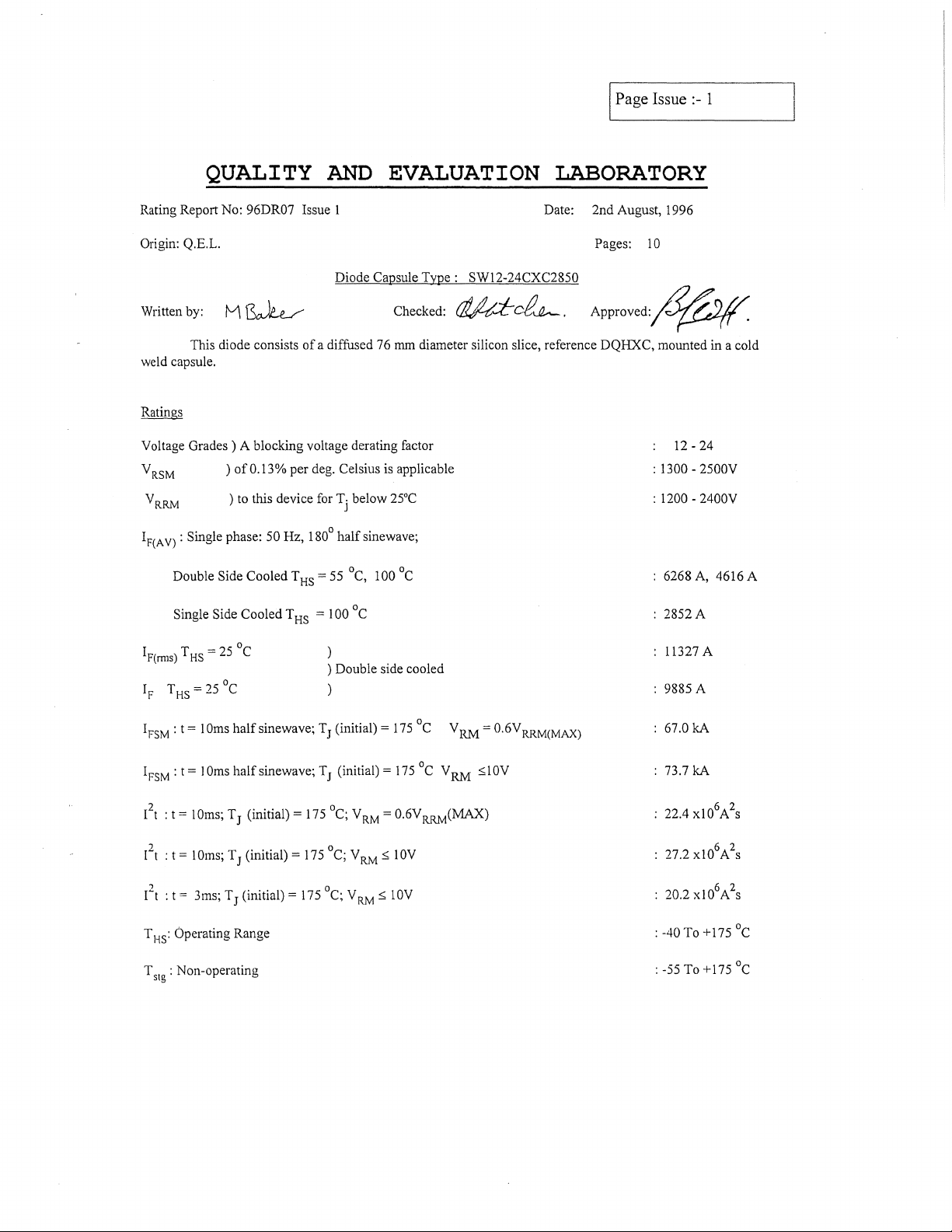
QUALITY
Rating Report No: 96DR07 Issue 1 Date: 2nd August, 1996
Origin: Q.E.L.
Written by: M
This diode consists
weld capsule.
Voltage Grades) A blocking voltage derating factor
V
RSM
V
RRN1
IF(AV) : Single phase: 50 Hz, 180
Double Side Cooled
Single Side Cooled T HS
13~
)
of
0.13% per deg. Celsius
)
to
this device for Tj below
of
a diffused 76
T
==
HS
==
AND
Diode Capsule
0
half
55°C,
100 ° C
EVALUATION
Checked:
mm
is
25°C
sinewave;
100
LABORATORY
Pages:
Type:
diameter silicon slice, reference DQHXC, mounted in a cold
applicable
°c
SW12-24CXC2850
C!Lf!t:.:t-ct~.
APproved:~
10
12
:
1300 - 2500V
: 1200 - 2400V
6268 A, 4616 A
2852A
- 24
I
: t
==
1
FSM
I
FSM
I2t : t = I
2
I
t : t = 10ms; T
T
HS
T
stg
Oms
: t = J
Oms
Oms;
: Operating Range
: Non-operating
) Double side cooled
half
sinewave; TJ (initial)
half sinewave; TJ (initial)
T J (initial) = 175°C; V
(initial) = 175°C; V
J
RM
RM
==
==
= 0.6V
$
175°C V
175
DC
V
RRM(MAX)
10V
RM
= 0.6V RRM(MAX)
RM
$IOV
11327 A
9885 A
67.0 kA
73.7
kA
: -40 To +175
:-5STo+17SoC
DC
Page 3
-2-
R.R.
No. : 96DR07/CXC2850
R.R.
Issue : I
Page
Issue : I
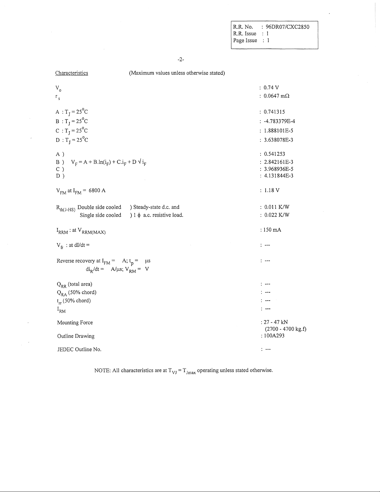
Characteristics
=
A : T
B : T
C : TJ= 25°C
D:T
25°C
J
= 25 C
J
=25°C
J
°
A )
B)
V F = A + B.ln(iF) + C.i
C )
D )
V
at
IFM
FM
l\h(J-HS)
IRRM
V
fr
=
Double
Single side
: at V
RRM(MAX)
: at dIldt =
6800
side
A
cooled
cooled
(Maximum
+ D
F
) Steady-state d.c. and
) I $ a.c. resistive load.
values unless otherwise stated)
"iF
0.74 V
0.0647
mn
0.741315
-4.783379E-4
1.888101E-5
3.638078E-3
0.541253
2.842161E-3
3.968936E-5
: 4.131844E-3
1.18
V
0.011
K/W
0.022
KlW
: 150
mA
Reverse recovery
diR/dt =
Q
(total area)
RR
Q
(50% chord)
RA
trr
(50% chord)
IRM
Mounting
Outline
JEDEC Outline No.
Force
Drawing
NOTE:
at
IFM
= A; tp =
AI~lS;
V
RM
All characteristics are at T
= V
~LS
VJ
= T
Jma
,{
operating
: 27
(2700 -
: 100A293
unless stated otherwise.
-47
kN
4700
kg.£)
Page 4
R.R.
No.
R.R.
Issue : 1
Page Issue : 1
- 3 -
CONTENTS
Ratings
Characteristics 2
: 96DR07/CXC2850
Contents
Voltage
Dissipation and Heatsink Temperature
Limit
Ratings 4
vs
Mean Current
Forward Voltage Characteristic
Transient Thermal Impedance Characteristic
Surge Current
and
12t
vs
Duration
of
Surge 9
Outline Drawing
3
5&6
7
8
10
Page 5

Voltage Ratings
R.R. No. : 96DR07/CXC2850
R.R. Issue : 1
Page Issue : 1
- 4 -
Voltage Class
12
14
16
18
20
22
24
1.
This Report
SaleslProduction.
2. A blocking voltage derating factor
is
applicable
to
higher or lower voltage grades when supply has been agreed
V
RRM
V V
1200
1400
1600 1700
1800 1900
2000 2100
2200 2300
2400
of
0.13% per deg. Celsius is applicable
V
RSM
l300
1500
2500
by
to
this device for TJ below
25
DC.
Page 6

14000
(j)12000
~
ell
~
§ 10000
:0
ell
0..
. iii
en
o
"0
"-
ell
2:
6000
o
lJ..
E
E 4000
.--------------.
Double Side Cooled
-------------
6 Phase
..
_---
_
..
-..
_-----
1
---.~.---~.---.~-
Phase d.c.
3 Phase
-----.----
:.
/---A-·-----·---·---·-fr--··--------
------,L~I
".--,,--.--:"-~
----
--,-----i----
-----------.---.----.
..
__
.......
_--------_.
Page
Page
R.R
No.
RR
Issue 1
No.
Issue 1
96DR07
5
2000----------
o
180
G'
o~
ci.
E
140
Q)
f-
.:;,c:
c
Ci5
120
..!-
ro
Q)
I
100
Q)
:0
'(ji
<fJ
80
'E
....
(I)
0.
E
60
::J
E
'x
ro
40
2
-_
..
_----
...
_-_ ....... -
..
--_....
...---------~---
..
-----
....
~---.
a 1000 2000 3000 4000 5000 6000 7000 8000 9000
_
..
-_._------------------
..
Mean Forward Current (Amps)
...
_---_
..
__
...
_ ...
_----
._-------_
(Whole
..
_-------_._-
--"
Cycle Averaged)
----------"
~~--.---
.. ----""
.-------.----
----r-
j
.._---
10000!
20
a
1000 2000 3000 4000 5000 6000 7000 8000 9000 10000
a
Mean Forward Current (Amps)
(Whole
Cycle Averaged)
Page 7

Single Side Cooled
Page
Page
RR
No.
R.R
Issue 1
No.
Issue 1
6
96DR07
7000--
(j)6000
::::
C1l
S
......,
c 5000
o
:;::;
C1l
0.
'w
c5
4000
-e
ctl
§ 3000
u..
E
::J
.~
2000
ctl
~
1 000
----------------
----
--------~----'--
~
c-
__
---------r--A"-/--
-
------------------:
6
Phase
i
1 Phase d.c.
3 Phase
i
I
!--I~---~
~
l---r-----+-~
!
----:----~
i
__
l
------------+-----i---
-,
, i '
!
, ,
+--~
, ,
~~~
t
t
o
---------------'--
o 500 1000 1500 2000 2500 3000 3500 4000 4500 5000 5500 6000
Mean Forward Current (Amps)
180 ----------------,---------------
.........
u
0......, 160
~
~
~
I
:0
'w
0.
E
c
C1l
(l)
(l)
r.n
'E
I-
m
0..
E
::J
E
'x
C1l
~
140
120
100 -
80
60-
40
20
-------""-"'''''
-----
----
---------------------
--~---
---------~
,
(Whole
----------
--+-----
, i
i-
Cycle
OJ
---~ -
ci
Averaged)
_:_-_··_··--1
--i-----!-
6500!
--------:----i
-------------;
0
"0
o
o 500 1000 1500 2000 2500 3000 3500 4000 4500 5000 5500 6000 6500
Mean Forward Current (Amps)
(Whole
Cycle Averaged)
Page 8

Page No. 7
Issue 1
Page
R.R. No.
R.R. Issue 1
96DR07
,--.,
(J)
(l)
"-
(!)
CL
E
«
........-
.......
c
(!)
"-
"-
::::J
U
'"0
"-
co
~
a
LL
(J)
::::J
a
(l)
c
co
.......
c
co
.......
(J)
c
Forward
----------------------_.----_.----
--------------------,------------------;----------~-__/7.q---,-------
----------
--_._---------,----.
---r------!"-----
---i'--~
1000 -
-----'---------;----'---
: -175 C
Characteristic
----------------
-.-
..
-.-.--~----'/"---,~--+-.-+--:---~--+---;
0
of
Limit
-------------:
-,----+---~--~-
Device
! i .
;r----:;r--------
! I
) , .
A = 0.541253
B = 2.842161E-3
C = 3.968936E-5
o =
= 0.741315
A
B = -4.783379EA
= 1.888101E-5
C
D = 3.638078E-3
-~-~-~
--'-:
4,
131844E-3
----;-----1
100
0,6 0.7
0.8
0,9
1.1
1,2
Maximum Instantaneous Forward Voltage (Volts)
1.3 1.4
Page 9

0.1
-
0.01
~
-
C1>
t.)
C
ca
"C
C1>
Co
E
ca
E
...
C1>
0.001
..c
t-
0.0001
0.001
/
Transient Themallmpedance (Junction to Heat Sink)
KIW
I--
-
v-
f"i-'"
.......
~
~
~
i..-'
/'
-
0.022
s.s.c.
0.011
D.S.C.
KIW
V
~
.......
.......
I..--'
V
V
~
V"
./
/
L-
_____
-
1.
-------
10
-
::0
?J
- z
!ll
c .
CD
.....
100
::0
?J
0
«>
(J)
o
::0
o
........
""0 ""0
I\)
to
to
CD
- z
!ll
c .
CD
.....
I\)
CD
0
(X)
0.01
-
0.1
---------
Time (Seconds)
Page 10

Maximum Non-Repetitive Surge Current
c:x:
....
c
e
...
:I
ON
OJ
C0 <{,
OJ
....
:I
(/)
OJ
N-
c
.-
(/)
~
:r:
X
C'\'l
Q)
a.
.s
o
f-
1000000
Cf)
0
..-
X
~
100000
E
:::l
.~
X
CO
~
~
10000
:1
. I
@ Initial Junction Temperature
175°C
I i
I
,
1.·
!
.[
I '
I
I I
I,··
i I
I~
i i
~~-i-i
~.r-i'N~~·
I·
..
-t
.
jl
.
I
.
:~IIII
1
3
is'
·f---·-·---·
-~
-II-~
-------T·
r----·--j-
r-rir----
i
.1
II
I I
Ii : i I
Ii
II
....
....
+.
-
1-"
·1·
I
~
.
I-+-'---f
Mf~.'''------··--''-ll-
I : I I
, !
11
I I I I
LUl
------..i
o
f
I !
'1
IJ
i-I-t'i'
.UJk
.--
....
"-1--'
t-L
I
11
J :
II
Iii
Ii
r-t
j
L
156
."
....
L
..
--------100.
2
I tVRRM =10V
2
I t:60%V
RRM
~.,
IFSMVRRM=10V
IFSM:60%V
RRM
..
;o;O"U"U
~;u~~
_.
1Z
c:
(J)
_1.
(J)
Z
CilZ
9 Cf) 0
CD
c:
(j)
(J)
0
;0
0
--.j
(J)
.
CD
Duration
of
Surge (ms)
Duration
of
Surge (Cycles @ 50 Hz)
Page 11

ACAU
Ktr:1
UUAL:J-l
TYPE
~!
l~nERNATIONAL
~!
G.A.
DWG
~i
WEIGHT.
::::1
~I
F!NISH.
~I
DEVICE
sir
CENTRE
:701
DISTRIBUTED
c:
SURFACES
~I
CLAMPING
~I~------------------------------------~--------------------~
i:51
iSl
~'I
~!
~II
IviOUNTING:
LINE
1·---·-----
i
III
OUTLINE
1\10.
159B100H601
I.
7kg
~'·J!CKEL
TO
FORCE
PLATE
CLAMPING
OF
LOCATlmJ
OVER
AREA
WHICH
DEVICE
= 3700±1000kgf.
/
i·lo.
FORCE
HOLES
OF
COI\ITACT.
IS
CLAMPED
//~-
///
/ /
,///---
-10-
TO
BE
AND
(37±
/.\,PPLIED
BE
EVENLY
FLAT
TOL.
TO
BE
IOkN)
--~
ON
0.04
ON
WiDE.
I
~~.....-------r-----,-'-......
_-----r----....
I
~~.
CXC974
CXCISC
CXCI8C
CXC20C
CXC21
CXC26C
CXC30C
~"
~
--......
.....
/",
C(C32C
CXC28S0
C
0.3.6/3.5x.3
DEPTH
/:~
2-HOLES,
~~b;~~E
\
NUMBER
MIN.
m1E
Ar~D
ONE
:11 /
~1
~I
~I
~
~
S I \ 1
~
I
QJ
~
;:;:
::2
61'
~
~
I!
~-J---~~-------
\;~J&~b,~PJ
\
~
: ?
/;/
~
"M~
41
~
I i
\ " 1
,",,"',
\
"\...~"
''''
....
........
""'~~~.--.__
I-
1
I
J
j
\
t
I
I
i.
:
X\\\
I / \
~
n L 1 r r
J
ll~J
"-........"~//
~~
Leu
I
I
rfJ73.1
±O.1
I
I
:
(~n··
o,li{ i
t;lA
/
//
//
vLj
/
/
____
~,/
-I
I
1
I
I
~:
•
I
I
(073.1
±O.·I
(~
,
;
j
;',
CREEP
OVER
CONVOLUTIONS
:::::
41.5
PATH
MIN.
--::ll.fll
~IUjj--r
~I::.i§;
~II
~I!~:
~
"I
~I
;::;;!
is'
i
Lf)
II.~
;z
E~i~)
POBOX
i,~
~
W I i
J co
WESTCODE
57, CHIPPENHAM,
TEL
0249
441000.
TELEFAX
SEMICONDUCTORS
WILTSHIRE,
0249
441250/659448.
SN15
UL,
LTD.,
ENGLAND.
I
J
Page 12

Drawing Number – W7
Outline Number – 100A293
Weight 1700g
Westcode Customer Services email: wsl.sales@westcode.com Telephone: +44 (0)1249 444524 Fax: +44 (0)1249 659448
Page 13

Drawing Number – W42
Outline Number – 100A310
Weight 1200g
Westcode Customer Services email: wsl.sales@westcode.com Telephone: +44 (0)1249 444524 Fax: +44 (0)1249 659448
 Loading...