

Page 1
®
VNQ05XSP16
QUAD CHAN NEL HIGH SIDE SOLID STATE RELAY
TYPE RON(*) I
OUT
V
CC
VNQ05XSP16 110mΩ 5A (*) 36 V
(*) Per each channel
■ OUTPUT CURRENT (CONTINUOUS): 5A
■ CMOS COMPATIBLE INPUTS
■ MULTIPLEXED PROPORTIONAL LOAD
CURRENT SENSE
■ UNDERVOLTAGE & OVERVOLTAGE
PowerSO-16
ORDER CODES
PACKAGE TUBE T&R
PowerSO-16™ VNQ05XSP16 VNQ05XSP1613TR
TM
SHUT- DOWN
■ OVERVOLTAGE CLAMP
■ THERMAL SHUT DOWN
■ CURRENT LIMITATION
■ VERY LOW STAND-BY POWER DISSIPATION
■ PROTECTION AGAINST:
n LOSS OF GROUND & LOSS OF V
■ REVERSE BATTERY PROTECTION (**)
CC
DESCRIPTION
The VNQ05XSP16 is a monolithic device
designed in STMicroelectronics VIPower M0-3
Technology. It is intende d for driving any type of
multiple loads with one side connec ted to grou nd.
Active V
against low energy spikes (see ISO7637 transient
pin voltage clamp protects the devi ce
CC
compatibility table). This device has four
independent channels and one multiplexed analog
sense output which del iver a current propor tional
to the selected output current. SenseEnable pin
allows to connect any number of VNQ05XSP16 on
the same Current Sense line. Active current
limitation combined with thermal shut-down and
automatic restart protect the device against
overload. Device automatically turns off in case of
ground pin disconnection.
ABSOLUTE MAXIMUM RATING
Symbol Parameter Value Unit
V
-V
I
OUT
I
I
V
CSENSE
I
GND
V
ESD
P
E
MAX
T
T
STG
T
Supply voltage (continuous) 41 V
CC
Reverse supply voltage (continuous) -0.3 V
CC
Output current (continuous), for each channel Internally limited A
Rever se output c urrent (c ontinuous), for each channel -5 A
R
Input current (IN1,IN2,IN3,IN4,SELA,SELB,SENSENABLE) +/- 10 mA
IN
Current sense maximum voltage
Ground current at T
<25°C (continuous) -200 mA
case
Electros tatic Discharge (H um an Body Mo del: R=1.5Ω; C=100pF )
- INPUT
- CURRENT SENSE
- OUTPU T
- V
CC
Power dissipation at T
tot
=25°C 78 W
case
Maximum Switching Energy
(L=1.72mH; R
Junction operating temperature Internally limited °C
j
Case Operating Temperature - 40 to 150 °C
c
=0Ω; V
L
=13.5V; T
bat
=150ºC; IL=7.5A)
jstart
Storage temperature -55 to 150 °C
-3
+15
4000
2000
5000
5000
76 mJ
V
V
V
V
V
V
(**) See appl ic ation schem atic at page 9
March 2 003 1/17
Page 2
VNQ05XSP16
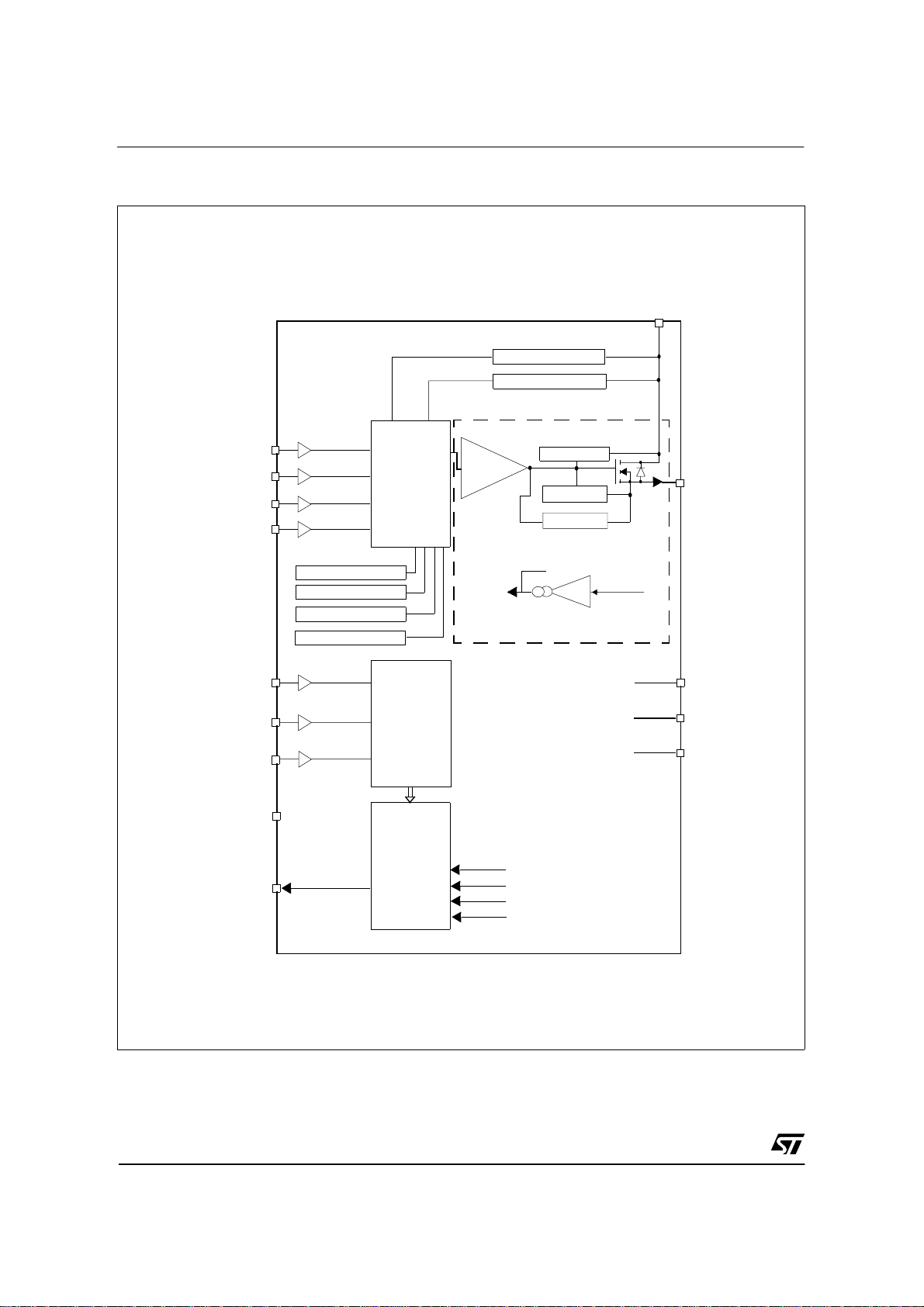
BLOCK DIAGRAM
OVERVOLTAGE
UNDERVOLT AGE
V
CC
INPUT 1
INPUT 2
INPUT 3
INPUT 4
SELECT A
SELECT B
SENSE ENABL E
GND
CURRENT SENSE
OVERTEMP . 1
OVERTEMP. 2
OVERTEMP. 3
OVERTEMP. 4
ANALO G
LOGIC
DIAG
LOGIC
QUAD
Mux
DRIVER 1
DEMAG
Ot
1
CS
1
Same structure for the channels2,3,4
I
Vds
1
LIM 1
LIM 1
K
CS1
CS2
CS3
CS4
I
OUT1
OUTPUT 1
OUTPUT 2
OUTPUT 3
OUTPUT 4
2/17
Page 3

CURRENT AND VOLTAGE CO NVENTIONS
I
IN1
I
V
SELB
V
IN2
I
IN3
I
IN4
I
SENSE
I
SELA
I
SELB
I
SENSENABLE
SENSENABLE
V
IN1
V
IN2
V
IN3
V
IN4
V
SENSE
V
SELA
INPUT1
INPUT2
INPUT3
INPUT4
V
CC
SENSE
SELA
SELB
SENSENABLE
GND
OUTPUT1
OUTPUT2
OUTPUT3
OUTPUT4
I
GND
I
S
I
OUT1
I
OUT2
I
OUT3
I
OUT4
V
OUT4
V
VNQ05XSP16
V
OUT2
OUT3
V
OUT1
V
CC
CONNECTION DIAGRAM ( TOP VIEW)
INPUT 1
INPUT 2
INPUT 3
INPUT 4
C.SENSE
SENSENABLE
SELA
SELB
V
CC
10
11
12
13
14
15
16
17
89
7
6
5
4
3
2
1
GROUND
N.C.
OUTPUT 1
OUTPUT 2
N.C.
OUTPUT 3
OUTPUT 4
V
CC
3/17
Page 4
VNQ05XSP16
THERMAL DATA
Symbol Parameter Value Unit
R
thj-case
R
thj-amb
Thermal resistance jun ction-case (MAX) 1.6 °C/W
Thermal resistance jun ction-a m bient (MAX) 51.6 (*) °C/W
(*) When mounted on FR4 printed circuit board with 0.5 cm² of copper area (at least 35 µm thick) connected to all V
CC
pins
ELECTRICAL CHARACTERISTICS (8V<VCC<36V; -4 0°C<Tj<150°C; unless o therwise specified) (Per each channel)
POWER
Symbol Parameter Test Conditions Min Typ Max Unit
V
V
USD
V
R
V
clamp
I
I
L(off1)
I
L(off2)
I
L(off3)
I
L(off4)
SWITCHING ( V
Operating supply voltage 5.5 13 36 V
CC
Under voltage shut down 3 4 5.5 V
Overvoltage shut down 36 V
OV
1,2,3,4=1A; Tj=25°C
I
OUT
On state resistan ce
ON
I
1,2,3,4=1A; Tj=150°C
OUT
I
1,2,3,4=0.5A; VCC=6V
OUT
Clam p Vo ltage ICC=20mA (See note 1) 41 48 55 V
CC
=13V
OUT
=0A;
Supply current
S
Off State Output Current VIN=V
Off State Output Current VIN=0V; V
Off State Output Current VIN=V
Off State Output Current VIN=V
=13V)
CC
Off state; Inputs=n.c.; V
On state; V
R
SENSE
=5V; VCC=13V; I
IN
=3.9k Ω
=0V 0 50 µA
OUT
=3.5V -75 0 µA
OUT
=0V; Vcc=13V; Tj=125°C 5 µA
OUT
=0V; Vcc=13V; Tj=25°C 3 µA
OUT
110
220
330
80
10
mΩ
mΩ
mΩ
µA
mA
Symbol Parameter Test Conditions Min Typ Max Unit
Turn-on delay tim e RL=2.6Ω channels 1,2,3,4 (see figure 2) 40 µs
Turn-off delay time RL=2.6Ω channels 1,2,3,4 (see figure 2) 40 µs
/
OUT
Turn-on voltage s lope RL=2.6Ω channels 1,2,3,4 (see figure 2)
on
/
OUT
Turn-off voltage slope RL=2.6Ω channels 1,2,3,4 (see figure 2)
off
See
relative
diagram
See
relative
diagram
V/µs
V/µs
(dV
(dV
t
d(on)
t
d(off)
dt)
dt)
PROTECTIONS
Symbol Parameter Test Conditions Min Typ Max Unit
I
lim
T
TSD
T
T
HYST
V
demag
V
ON
Note 1: V
=13V
V
DC short circuit current
CC
5.5V<V
CC
<36V
Thermal shut down
temperature
Thermal reset
R
temperature
Ther m al hy steresis 715 °C
Turn-off output voltage
clamp
Output voltage dr op
limitation
and VOV are correlated. Typical difference is 5V.
clamp
I
=2A; L=6mH VCC-41 VCC-48 VCC-55 V
OUT
I
=0.1A
OUT
T
=-40°C...+150°C
j
57.51010A
150 175 200 °C
135 °C
50 mV
4/17
1
A
Page 5
VNQ05XSP16
CURRENT SENSE (9V< VCC <16V)
Symbol Parameter Test Conditions Min Typ Max Unit
I
K
1
dK
1/K1
K
2
dK
2/K2
K
3
dK
3/K3
I
SENSEO
V
SENSE1,2,3,4
I
OUT/ISENSE
Current Sense Ratio
Drift
I
OUT/ISENSE
Current Sense Ratio
Drift
I
OUT/ISENSE
Current Sense Ratio
Drift
Analog Sense
Leakage Current
Max analog sense
output voltage
Analog sense output
V
SENSEH
voltage in
overtemperature
condition
Analog sense output
R
VSENSEH
impe da nc e i n
overt em p erature
condition
t
DSENSE
Current sense delay
=0.1A; V
OUT
T
=-40...+150°C
j
I
=0.1A; V
OUT
T
= -40°C...+150°C
j
I
=1.0A, V
OUT
T
=-40...+150°C
j
I
=1.0A; V
OUT
T
=-40°C...+150°C
j
I
=2.0A, V
OUT
T
=-40...+150°C
j
I
=2.0A; V
OUT
T
=-40°C...+150°C
j
VCC=6...16V;
I
=0A;V
OUT
T
=-40°C...+150°C
j
V
CC
R
SENSE
V
CC
R
SENSE
=5.5V, I
=10kΩ
>8V, I
=10kΩ
SENSE
OUT1,2,3,4
VCC=13V; R
=13V; Tj>T
V
CC
All Channels Open
V
=13V; R
CC
(see note 2)
=0.5V
SENSE
SENSE
SENSE
SENSE
SENSE
SENSE
=0V;
OUT1,2,3,4
=0.5V;
=4V
=4V;
=4V
=4V;
=1.0A
650 950 1200
-10 +10 %
800 1000 1200
-8 +8 %
850 1000 1150
-6 +6 %
010µA
2
=2.0A
4
= 3.9kΩ 5.5 V
SENSE
;
TSD
SENSE
=3.9kΩ
400 Ω
300 500 µs
V
V
LOGIC CHARACTERISTICS (Inputs, Sela&b, Sensenable)
Symbol Parameter Test Conditions Min Typ Max Unit
V
IL
V
IH
V
I(hyst)
I
IL
I
IN
V
ICL
Note 2: current sense signal delay after pos itive input sl ope.
Note: Sense pin doesn’t have to be left float ing.
Inpu t low level
voltage
Input high level
voltage
Input hysteres is
voltage
Low level input
current
High level inp u t
current
Input clamp voltage
=1.25V 1 µA
V
IN
VIN=3.25V 10 µA
I
=1mA
IN
I
=-1mA
IN
3.25 V
0.5 V
66.8
-0.7
1.25 V
8V
V
5/17
2
Page 6
VNQ05XSP16
TRUTH TABLE
CONDITIONS INPUT OUTPUT SENSE
Normal op eration
Overtemperature
Undervoltage
Overvoltage
L
H
L
H
L
H
L
H
L
Short circuit to GND
H
H
Short circuit to V
CC
Negative output voltage
clamp
L
H
LL 0
TRUTH TABLE
SENSENABLE SELB SELA SENSE
L X X High Impedance
HL LI
HL HI
HH LI
HH HI
Figure 1: I
OUT/ISENSE
versus I
OUT
L
H
L
L
L
L
L
L
L
L
L
(T
(T
H
H
0
Nominal
0
V
SENSEH
0
0
0
0
0
) 0
j<TTSD
) V
j>TTSD
SENSEH
0
< Nomin a l
SENSE=IOUT1
SENSE=IOUT2
SENSE=IOUT3
SENSE=IOUT4
/K
/K
/K
/K
6/17
1
I
OUT/ISENSE
1500
1400
1300
1200
1100
1000
900
800
700
600
500
012345678910
I
(A )
OUT
max. T j= -4 0°C< < 150°C
typical value
min. T j= - 40 ° C< <150°
C
Page 7

ELECTRICAL TRANS IENT REQUIREMENTS
ISO T/R
7637/1
Test Pulse
1 -25V -50V -75V -100V 2ms, 10Ω
2 +25V +50V +75V +100V 0.2ms, 1 0Ω
3a -25V -50V -100V -150V 0.1µs, 50Ω
3b +25V +50V +75V +100V 0.1µs, 50 Ω
4 -4V -5V -6V -7V 10 m s, 0.01Ω
5 +26.5V +46.5V +66. 5V +86.5V 400 m s, 2Ω
Test LevelsITest LevelsIITest Levels
VNQ05XSP16
Test Levels
III
IV
Test Levels
Delays and Impedance
ISO T/R
7637/1
Test Levels ResultITest Levels ResultIITest Levels Result
Test Pulse
1 CCCC
2CC CC
3a CCCC
3b CCCC
4CC CC
5CE EE
Class Contents
C All functions of the device are performed as designed after expo sure to dis turbance.
E
One or more funct i ons of the device is not performed as designed after exposure a nd cannot be
returned to prop er operation without replacing the de vice.
Figur e 2: Switching Characteristics (Resistive load RL=1.3Ω)
V
OUT
80%
dV
/dt
OUT
(on)
10%
I
SENSE
t
r
90%
t
f
dV
OUT
III
/dt
Test Levels Result
IV
(off)
t
INPUT
t
d(on)
90%
t
DSENSE
t
d(off)
t
t
7/17
1
Page 8

VNQ05XSP16
Figur e 3: Waveforms
INPUT
1
LOAD CURREN T
SENSE
1
SENSEN
V
CC
INPUT
1
LOAD CURRENT
SENSE
1
SENSEN
V
CC
INPUT
1
LOAD CURRENT
SENSE
1
SENSEN
NORMAL OPERATION (for example: Channel1 is ON)
1
UNDERVOLT AGE
V
USDhyst
V
USD
1
OVERVOLTAGE
V
OV
VCC < V
OV
1
VCC > V
OV
INPUT
1
LOAD CURRENT
LOAD VOLTAGE
SENSE
1
SENSEN
INPUT
1
LOAD VOLTAGE
LOAD CURREN T
SENSE
1
SENSEN
T
j
INPUT
1
LOAD CURRENT
SENSE
1
SENSEN
SHORT TO GROUND
1
1
SHORT TO V
1
1
<Nominal
T
TSD
T
R
1
OVERTEMPE RATURE
CC
<Nominal
I
SENSE
=
V
SENSEH
R
SENSE
8/17
1
Page 9

APPLICATION SCHEMAT IC
+5V
R
prot
R
prot
R
prot
R
C
FILT ER
prot
R
prot
R
prot
R
prot
R
prot
C
PAR
R
µ
C
A/D
SENSE
INPUT1
INPUT2
INPUT3
INPUT4
SELA
SESB
SENSENABLE
C. SENSE
GND
R
GND
VNQ05XSP16
V
CC
D
ld
OUTPUT1
OUTPUT2
OUTPUT3
OUTPUT4
V
GND
GND
D
Notes: Input1,2,3,4, SELA, SELB, SENSENABLE have the same structure.
R
x C
SENSE
GND PROTECTION NETWORK AGAINST
REVERSE BATTE RY
Solutio n 1: Resis tor in the gr ound line (R
can be use d with any t ype of load .
The foll owing is a n indicatio n on how to d imension th e
resistor.
R
GND
1) R
2) R
where -I
be found i n the absol ute maxi mum rating section of the
device’s datasheet.
Power Dissipation in R
batter y si t uations) i s:
P
D
This resistor can be shared amongst several different
HSD. Please note that the value of this resistor should be
calcula ted wit h formul a (1) where I
sum of the maximum on-state currents of the different
devices.
Please note that if the microprocessor ground is not
common with the device ground then the R
produce a shi ft (I
and the status output values. This shift will vary
dependin g on how m any d evices are O N in the case o f
several high side drivers sharing the same R
If the calculated power dissipation leads to a large
resistor or several devices have to share the same
resistor then the ST suggests to utilize Solution 2 (see
below).
≤ 600mV / (I
GND
≥ (-VCC) / (-I
GND
is the D C re ver se gr ou nd p in curr ent a nd c an
GND
= (-VCC)2/R
GND
S(on)m ax
<10µs
PAR
GND
).
S(on)max
)
GND
(when VCC<0: during reverse
GND
becomes the
S(on)max
* R
) in the i nput t hres ho lds
GND
GND
only). This
will
GND
.
Soluti o n 2:
A resistor (R
D
if the devi ce will be driving an inductive load.
GND
This small signal diode can be safely shared amongst
several d iffer en t HSD. Als o i n thi s ca se , the pr esen ce of
the ground network will produce a shift (≅600mV) in the
input threshold and the status output values if the
micropr ocessor ground is not common with the device
ground. This shift will not vary if more than one HSD
shares the same diode/resistor network.
LOAD DUMP PROTECTION
Dld is nece ssary (Voltage Transient Suppressor) if the
load dump peak voltage exceeds VCC max DC rating.
The same applies if the device will be subject to
transients on the VCC line tha t are gr eate r tha n th e ones
shown in the ISO T/R 7637/1 table.
µC I/Os PROTECTION:
If a ground protection network is used and negative
transi ents are pre sent on the VCC line, the co ntrol pins
will be pu lled negati ve. ST suggests to insert a resi stor
(R
) in lin e to prevent the µC I/Os pins to latch-up.
prot
The value of these resistors is a compromise between the
leakage current of µC and the current requ ired by the
HSD I/Os (Input levels compatibility) with the latch-up
limit of µC I/Os.
-V
CCpeak/Ilatchup
For V
CCpeak
5kΩ ≤ R
Recommended R
A diode (D
GND
= - 100V and I
≤ 65kΩ.
prot
) in the gr ound line.
GND
=1kΩ) should be inserted in parallel to
≤ R
≤ (V
prot
value is 10kΩ.
prot
OHµC-VIH-VGND
≥ 20mA; V
latchup
) / I
OHµC
IHmax
≥ 4.5V
9/17
1
Page 10

VNQ05XSP16
Off State Output Current
IL(off) (µA)
5
4.5
4
3.5
3
2.5
2
1.5
1
0.5
0
-50 -25 0 25 50 75 100 125 150 175
Off state
Vcc=36V
Vin=Vout=0V
Tc (ºC)
Input Clamp Voltage
Vicl (V)
8
7.75
7.5
7.25
7
6.75
6.5
6.25
6
Iin=1mA
-50 -25 0 25 50 75 100 125 150 175
Tc (ºC)
High Level Input Current
Iih (µA)
5
4.5
3.5
2.5
1.5
0.5
Vin=3.25V
4
3
2
1
0
-50 -25 0 25 50 75 100 125 150 175
Input High Level
Vih (V)
3.6
3.4
3.2
3
2.8
2.6
2.4
2.2
2
-50 -25 0 25 50 75 100 125 150 175
Tc (ºC)
Tc (ºC)
Overvoltage Shutdown
Vov (V)
50
47.5
45
42.5
40
37.5
35
32.5
30
-50 -25 0 25 50 75 100 125 150 175
10/17
1
Tc (ºC)
I
LIM
Vs T
case
Ilim (A)
20
17.5
15
12.5
10
7.5
2.5
Vcc=13V
5
0
-50 -25 0 25 50 75 100 125 150 175
Tc (ºC)
Page 11

Turn-on Voltage Slope Turn-off Voltage Slope
VNQ05XSP16
dVout/dt(on) (V/ms)
500
450
400
350
300
250
200
150
100
50
Vcc=13V
Rl=2.6Ohm
0
-50 -25 0 25 50 75 100 125 150 175
Tc (ºC)
On State Resistance Vs T
case
Ron (mOhm)
250
225
200
175
150
125
100
75
50
25
0
-50 -25 0 25 50 75 100 125 150 175
Iout=1A
Vcc=8V & 36V
Tc (ºC)
dVout/dt(off) (V/ms)
600
550
500
450
400
350
300
250
200
150
100
50
Vcc=13V
Rl=2.6Ohm
0
-50 -25 0 25 50 75 100 125 150 175
Tc (ºC)
On State Resistance Vs V
CC
Ron (mOhm)
200
175
150
125
100
75
50
25
0
5 10152025303540
Vcc (V)
Tc=150ºC
Iout=1A
Tc= 25ºC
Tc=-40ºC
11/17
1
Page 12

VNQ05XSP16
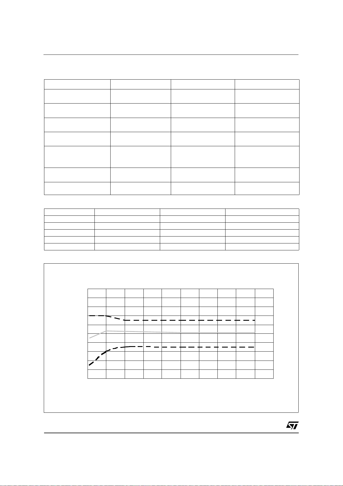
Maximum turn off current versus load inductance
LMAX (A)
I
100
10
1
0.01 0.1 1 10
A = Single Pulse at T
B= Repetitive pulse at T
C= Repetitive Pulse at T
Conditions:
VCC=13.5V
Values are generated with RL=0Ω
In case of repetitive pulses, T
the temperature specified above for curves B and C.
Jstart
=150ºC
Jstart
Jstart
=100ºC
=125ºC
(at beginning of each demagnetization) of every pulse must not exceed
jstart
A
B
C
L(mH)
VIN, I
12/17
1
L
Demagnetization
Demagnetization
Demagnetization
t
Page 13

PowerSO-16™ PC Board
VNQ05XSP16
PowerSO-16™ THERMAL DATA
R
thj-amb
Layout conditio n of Rth and Zth measurements (PCB FR 4 area= 60mm x 60mm, PCB thickness=2mm,
Cu thickness=35µm, Copper areas: 6cm
Vs PCB copper area in open box free air condition
2
).
RTHj_amb (°C/W)
55
Tj-Tamb=50°C
50
45
40
35
30
0246810
PCB Cu heatsink area (cm^2)
13/17
1
Page 14

VNQ05XSP16
Thermal Impedance Junction Ambient Single Pulse
ZTH (°C/W)
1000
100
10
1
0.1
0.0001 0.001 0.01 0.1 1 10 100 1000
Time (s)
Thermal fitting model of a quad HSD in
PowerSO-16
Tj_1
Pd1
Tj_2
Tj_3
Pd3
Tj_4
C1
C13 C14
R13
Pd2
C7
C15 C16
R15
Pd4
R14
R16
C3 C4
R3R1 R6R5R2
R17
R8
R18
C9 C1 0
R9R7
T_amb
C5 C6C2
R4
C11 C12C8
R10
R12R11
Pulse calculation formula
Z
THδ
where
RTHδ Z
δ tpT⁄=
THtp
Thermal Paramet er
Area/island (cm2) Footprint 6
R1 (°C/W) 0.18
R2 (°C/W) 0.8
R3 ( °C/W) 0.7
R4 (°C/W) 0.8
R5 (°C/W) 13
R6 (°C/W) 37 22
C1 (W.s/°C) 0.0006
C2 (W.s/°C) 1.50E-03
C3 (W.s/°C) 1.75E-02
C4 (W.s/°C) 0.4
C5 (W.s/°C) 0.75
C6 (W.s/°C) 3 5
Footprint
2
6 cm
1 δ–()+⋅=
14/17
1
Page 15

POWERSO-16TM MECHANICAL DATA
VNQ05XSP16
DIM.
A1 0 0.05 0.1
A2 3.4 3.5 3.6
A3 1.2 1.3 1.4
A4 0.15 0.2 0.25
a0.2
b 0.27 0.35 0.43
c 0.23 0.27 0.32
D 9.4 9.5 9.6
D1 7.4 7.5 7.6
d 0 0.05 0.1
E (1) 13.85 14.1 14.35
E1 9.3 9.4 9.5
E2 7.3 7.4 7.5
E3 5.9 6.1 6.3
e0.8
e1 5.6
F0.5
G1.2
L 0 .8 1 1.1
R1 0.25
R2 0.8
T 2° 5° 8°
T1 6° (typ .)
T2 10° (typ.)
Package Weight (typ.)
MIN. TYP MAX.
mm.
P013Q
15/17
Page 16

VNQ05XSP16
PowerSO-16™ SUGGESTED PAD LAYOUT
0.8 +/- 0.1
2 +/- 0.14
0.5 +/- 0.1
10 +/- 0.1
10.5 +/- 0.1
7.4 +/- 0.1
TAPE AND REEL SHIPMENT (suf fix “13TR”)
TUBE SHIPMENT (no suffix)
A
B
All dimensions are in mm.
Base Q.ty Bulk Q.ty Tube length (± 0.5) A B C (± 0.1)
50 1000 532 4.9 17.2 0.8
C
REEL DIMENSIONS
Base Q.ty 600
Bulk Q.ty 600
A (max) 330
B (min) 1.5
C (± 0.2) 13
F 20.2
G (+ 2 / -0) 24.4
N (min) 60
T (max) 30.4
TAPE DIMENSIONS
According to Electronic Industries Association
(EIA) Standard 481 rev. A, Feb. 1986
Tape width W 24
Tape Hole Spacing P0 (± 0.1) 4
Component Spacing P 24
Hole Diameter D (± 0.1/-0) 1.5
Hole Diameter D1 (mi n) 1.5
Hole Position F (± 0.05) 11.5
Compartm ent Depth K (max) 6.5
Hole Spacing P1 (± 0.1) 2
All dimensions are in mm.
Top
cover
tape
End
500mm min
All dimensions are in mm.
Empty components pockets
saled with cover tape.
User direction of feed
Start
No componentsNo components Components
500mm min
16/17
1
Page 17

VNQ05XSP16
Information furnish ed is believed to be accurate and r eliable. Ho wev er, S TMicroelect r onics assume s no r es ponsibility for the consequenc es
of use of such information nor for any infringement of patents or other rights of third parties which may results from its use. No license is
granted by implication or o therwise under any patent or patent rights of STMicroelect r onics. Specif ic ations mentioned in this publication are
subject to c hange withou t notice. This publication supersed es and replace s all information previo us ly s upplied. ST M icroelect r on ics products
are not authorized for use as critical components in life support devices or systems without express written approval of STMicroelectronics.
Australia - Brazil - Canada - Ch ina - Finland - Fr anc e - Germany - Hong K ong - India - Isra el - Italy - Jap an - M alaysia -
Malta - Morocco - Singapore - Spain - Sweden - Switzerland - United Kingdom - U.S.A.
The ST logo is a trademark of STMicroele c tronics
2003 STMicroelectronics - Printed in ITALY- All Rights Reserved.
STMicroelectronics GROUP OF COMPANIES
http://www.st.com
17/17
1
 Loading...