

Page 1
VN21
ISO HIGH SIDE SMART POWER SOLID STATE RELAY
PRELIMINARY DATA
TYPE V
VN21 60 V 0.05 Ω 7 A 26 V
■ MAXIMUM CONTINUOUS OUTPUT
DSS
R
DS(on)
In(*) V
CC
CURRENT (#): 23 A @ Tc=85oC
■ 5V LOGIC LEVEL COMPATIBLEINPUT
■ THERMAL SHUT-DOWN
■ UNDER VOLTAGE PROTECTION
■ OPEN DRAIN DIAGNOSTIC OUTPUT
■ INDUCTIVELOADFAST DEMAGNETIZATION
■ VERYLOWSTAND-BY POWER DISSIPATION
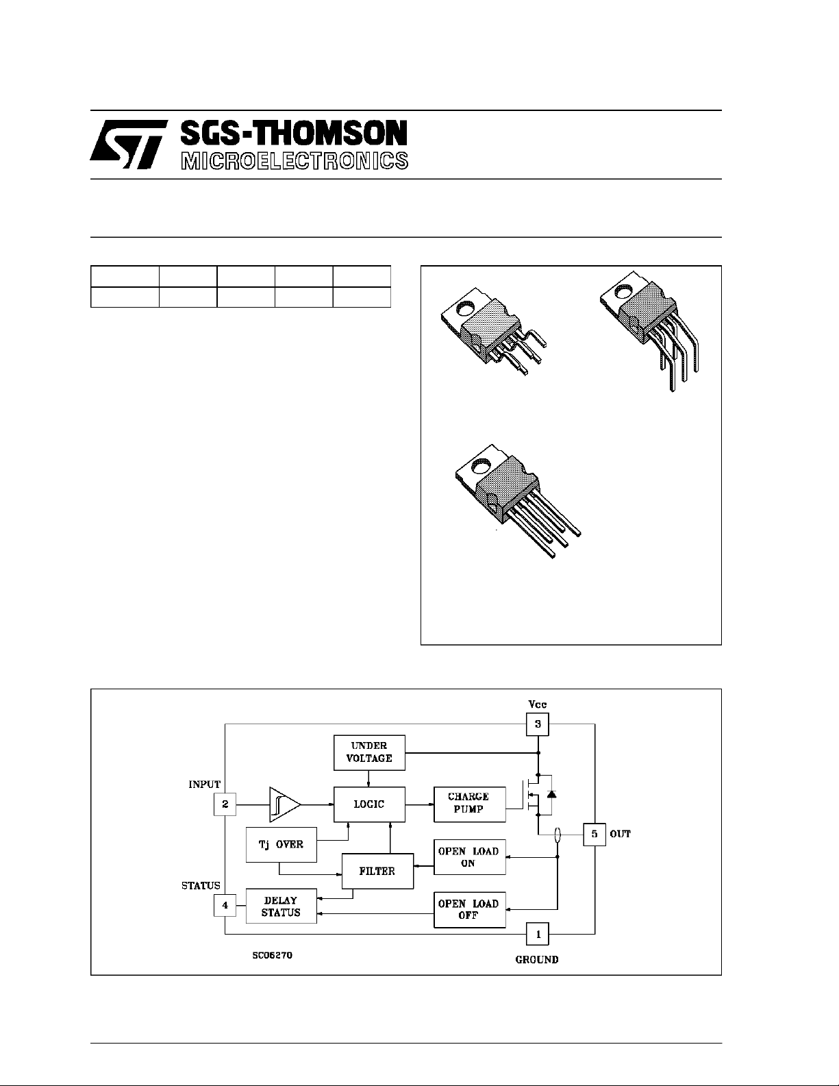
DESCRIPTION
The VN21 is a monolithic device made using
SGS-THOMSON Vertical Intelligent Power
Technology, intended for driving resistive or
inductive loads with one side grounded.
Built-in thermal shut-down protects the chip from
over temperature and short circuit.
The open drain diagnostic output indicates: open
load in off state and in on state, output shorted to
VCCand overtemperature. Fast demagnetization
of inductive loads is archieved by negative (-18V)
load voltage at turn-off.
BLOCK DIAGRAM
PENTAWATT
(vertical)
PENTAWATT
(horizontal)
PENTAWATT
(in-line)
ORDER CODES:
PENTAWATT vertical VN21
PENTAWATT horizontal VN21 (011Y)
PENTAWATT in-line VN21 (012Y)
(*) In= Nominal current accor ding to ISO defini t ion f or high side automoti ve swit ch (see note 1)
(#) The maximum conti nuous out put current i s the current at Tc=85oC for a battery voltage of 13 V whi ch does not ac tivate
sel f protection
September 1994
1/11
Page 2
VN21
ABSOLUTE MAXIMUM RATING
Symbol Parameter Value Uni t
V
(BR)DSS
I
OUT
I
I
-V
I
STAT
V
ESD
P
T
T
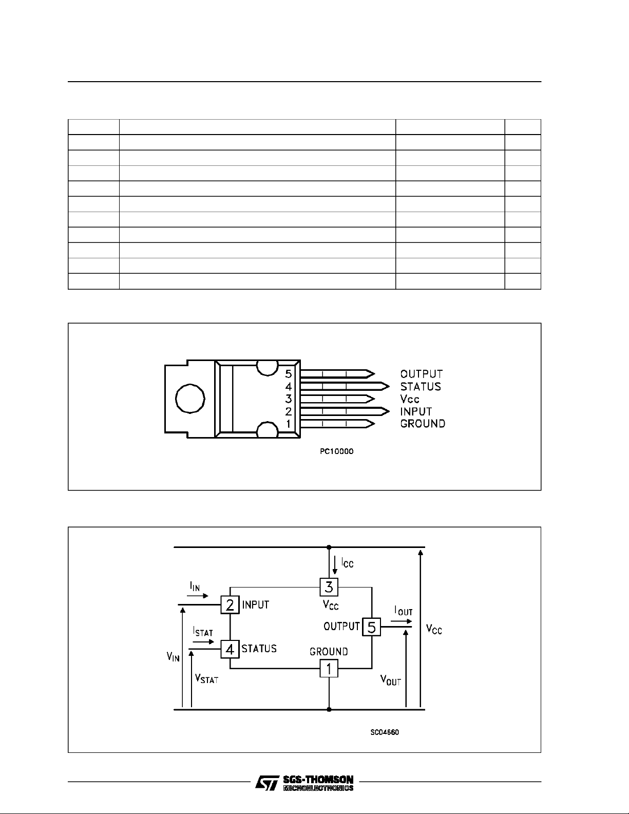
CONNECTION DIAGRAM
Drain - So urc e Bre ak dow n Voltage 60 V
Out put Current (co nt . ) at Tc=85oC23A
Reverse Outpu t Cur r ent at Tc=85oC-23A
R
Input Curre nt ±10 mA
IN
Reverse S upply V olt age -4 V
CC
St at us Current ±10 mA
Electrost atic Dischar ge (1.5 kΩ , 100 pF ) 2000 V
Powe r Diss i pation at Tc=85oC48W
tot
Junction Op erating Temper at ur e -40 to 150
j
St or a ge Te mperat ur e -55 to 150
stg
o
C
o
C
CURRENT AND VOLTAGE CONVENTIONS
2/11
Page 3

THERMAL DATA
R
thj-case
R
thj-amb
Thermal Resis tance Junction - cas e Max
Thermal Resistance Junction - ambient Max
1.35
60
ELECTRICAL CHARACTERISTICS (VCC= 13 V; -40 ≤ Tj≤ 125oC unless otherwise specified)
POWER
Symbol Parameter Test Condition s Min. Typ. Max. Unit
V
In( *) Nominal Curr ent T
R
I
V
DS(MAX)
Supply Voltage 5. 5 13 2 6 V
CC
=85oCV
c
On State Resistance I
on
Supply Current Of f S ta te Tj≥ 25oC
S
=7A
OUT
I
=7A Tj=25oC
OUT
≤ 0.5 (note 1) 7 A
DS(on)
On State
Maximum Volt age Drop I
=20A Tc=85oC1.8V
OUT
0.10
0.05
50
15
SWITCHING
Symbol Parameter Test Condition s Min. Typ. Max. Unit
(^) Tur n - on Delay T ime Of
t
d(on)
Out put Current
(^) Rise Ti m e Of Output
t
r
Current
(^) Tur n-off Delay Tim e Of
t
d(off)
Out put Current
(^) Fall T ime Of Out put
t
f
Current
(di/dt)
(di/dt)
V
demag
Turn-on C urrent S lope I
on
Turn-off Current Slope I
off
Inductive Load Clamp
Volt age
I
= 7 A Resist ive Lo ad
OUT
60 µs
Input Rise Time < 0.1 µs
I
= 7 A Resist ive Lo ad
OUT
70 µs
Input Rise Time < 0.1 µs
I
= 7 A Resist ive Lo ad
OUT
90 µs
Input Rise Time < 0.1 µs
I
= 7 A Resist ive Lo ad
OUT
25 µs
Input Rise Time < 0.1 µs
=7A
OUT
I
OUT=IOV
=7A
OUT
I
OUT=IOV
I
= 7 A L = 1 mH -24 -18 -14 V
OUT
0.08 0.51A/µs
0.2 3
3
VN21
o
C/W
o
C/W
Ω
Ω
µA
mA
A/µs
A/µs
A/µs
LOGIC INPUT
Symbol Parameter Test Condition s Min. Typ. Max. Unit
V
IL
V
IH
V
I(hyst.)
I
IN
V
ICL
Input Low Level
Volt age
Input High Level
Volt age
Input Hys teresis
Volt age
Input Curre nt VIN=5V
VIN=2V
VIN=0.8V 25
Input Clamp Volta ge IIN=10mA
IIN=-10mA
2(•)V
0.5 V
250 500
5.5 6
-0.7 -0.3
0.8 V
250
µA
µA
µA
V
V
3/11
Page 4
VN21
ELECTRICAL CHARACTERISTICS (continued)
PROTECTION AND DIAGNOSTICS(continued)
Symbol Parameter Test Condition s Min. Typ. Max. Unit
V
STAT
St at us Voltage Outp ut
Low
V
USD
Under V olt age Shut
Down
V
SCL
I
OV
I
AV
St at us Clamp Volt age I
Ove r Curr ent R
Aver age Current in
Short C ircuit
I
OL
Open Load Cur rent
Level
T
TSD
Thermal Shut-down
Tem perature
T
V
Reset T emperat ur e 125
R
Open Load Vol ta ge
OL
Level
t
1(on)
Open Load Fi lt er ing
Time
t
1(off)
Open Load Fi lt er ing
Time
t
2(off)
Open Load Fi lt er ing
Time
t
povl
t
pol
(^) See Switchig Time Waveforms
(•)TheVIHis internal ly clamped at 6V about. It is possible to c onnect this pin to an higher voltage via an external r es istor
cal culated to not exceed 10 mA at the i nput pin.
note 1: The Nominal Cur rent is the current at Tc=85oC for battery voltage of 13V w hich produces a voltage drop of 0.5 V
note 2: I
note 3: t
St at us Delay (not e 3) 5 10 µs
St at us Delay (not e 3) 50 700 µs
=(VCC-VOL)/ROL(see figure)
OL(off)
: minimum open load duration which acctivates the status output
1(on)
t
: minimum load recovery t ime which desactiv ates t he status output
1(off)
t
: minimum on time after thermal shut down which desactivates status output
2(off)
t
: ISO def inition (see figur e)
povltpol
I
=1.6mA 0.4 V
STAT
5V
=10mA
STAT
I
=-10mA
STAT
<10mΩ -40 ≤ Tc≤ 125oC 140 A
LOAD
R
<10mΩ Tc=85oC2.5A
LOAD
6
-0.7
5 300 700 mA
140
Off-State (note 2) 2.5 3.75 5 V
(note 3) 1 5 10 ms
(note 3) 1 5 10 ms
(note 3) 1 5 10 ms
V
V
o
C
o
C
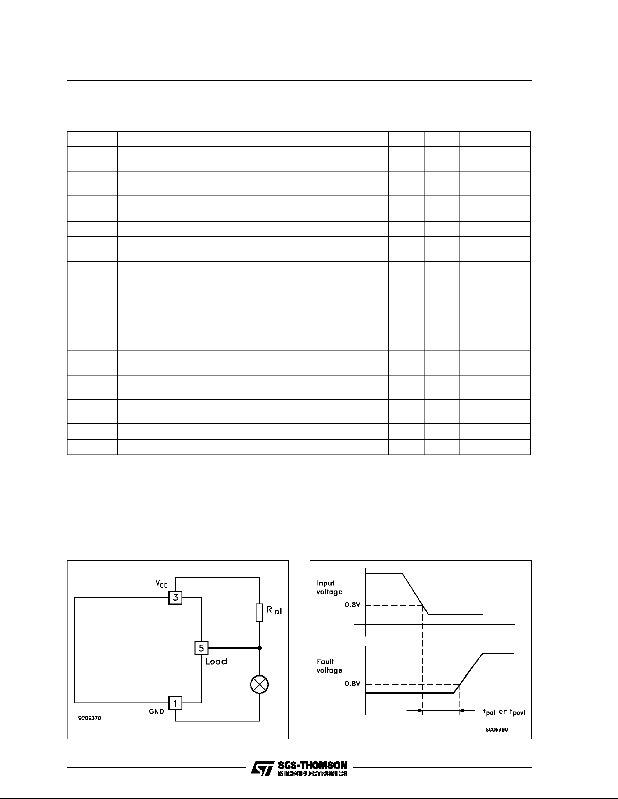
Note 2 Relevant Figure Note 3 Relevant Figure
4/11
Page 5

VN21
Switching Time Waveforms
FUNCTIONAL DESCRIPTION
The device has a diagnostic output which
indicates open load conditions in off state as well
as in on state, output shorted to VCCand
overtemperature. The truth table shows input,
diagnostic and output voltage level in normal
operation and in fault conditions. The output
signals are processed by internal logic. The
open load diagnostic output has a 5 ms filtering.
The filter gives a continuous signal for the fault
condition after an initial delay of about 5 ms. This
means that a disconnection during normal
operation, with a duration of less than 5 ms does
not affect the status output. Equally, any
re-connection of less than 5 ms during a
disconnection duration does not affect the status
output. No delay occur for the status to go low in
case of overtemperature conditions. From the
falling edge of the input signal the status output
initially low in fault condition (over temperature or
open load) will go back with a delay (t
of overtemperature condition and a delay (t
)in case
povl
pol
)in
case of open load. These feature fully comply
with International Standard Office (I.S.O.)
requirement for automotive High Side Driver.
To protect the device against short circuit and
over current conditions, the thermal protection
turns the integrated Power MOS off at a
minimum junction temperature of 140oC.
When the temperature returns to 125oC the
switch is automatically turned on again. In short
circuit the protection reacts with virtually no
delay, the sensor being located in the region of
the die where the heat is generated. Driving
inductive loads, an internal function of the
device ensures the fast demagnetization with a
typical voltage(V
demag
) of -18V.
This function allows to greatly reduce the power
dissipation according to the formula:
P
dem
=0.5•L
load
• (I
load
)2• [(VCC+V
demag
)/V
demag
]• f
where f = switching frequency and
V
= demagnetization voltage
demag
Based on this formula it is possible to know
the value of inductance and/or current to avoid
a thermal shut-down. The maximum inductance
which causes the chip temperature to reach the
shut down temperature in a specific thermal
environment, is infact a function of the load
current for a fixed VCC,V
demag
and f.
PROTECTING THE DEVICE AGAIST LOAD
DUMP - TEST PULSE 5
The device is able to withstand the test pulse
No. 5 at level II (Vs= 46.5V) according to the
ISO T/R 7637/1 without any external
component. This means that all functions of the
device are performed as designed after
exposure to disturbance at level II. The VN21 is
able to withstand the test pulse No.5 at level III
adding an external resistor of 150 ohm between
pin 1 and ground plus a filter capacitor of 1000
µF between pin 3 and ground (if R
LOAD
≤ 20 Ω).
PROTECTING THE DEVICE AGAINST
REVERSE BATTERY
The simplest way to protect the device against a
continuous reverse battery voltage (-26V) is to
insert a Schottky diode between pin 1(GND) and
ground, as shown in the typical application circuit
(fig.3).
The consequences of the voltage drop across
this diode are as follows:
– If the input is pulled to power GND, a negative
voltage of -Vfis seen by the device. (Vil, Vih
thresholds and Vstat are increased by Vf with
respect to power GND).
– The undervoltage shutdown level is increa-
sed by Vf.
If there is no need for the control unit to handle
external analog signals referred to the power
GND, the best approach is to connect the
reference potential of the control unit to node [1]
(see application circuit in fig. 4), which becomes
the common signal GND for the whole control
board avoiding shift of Vih,Viland V
stat
. This
solution allows the use of a standard diode.
5/11
Page 6

VN21
TRUTH TABLE
INPUT OUTPU T DIAGNO ST IC
Normal O per at ion L
H
Open C ircuit (No Load) H H L
Ove r -temperature H L L
Under-v oltage X L H
Short load to V
CC
LHL
Figure 1: Waveforms
L
H
H
H
Figure 2: Over Current Test Circuit
6/11
Page 7

Figure 3: Typical ApplicationCircuit With A Schottky Diode For Reverse Supply Protection
VN21
Figure 4: Typical ApplicationCircuit With Separate Signal Ground
7/11
Page 8

VN21
Pentawatt (vertical) MECHANICAL DATA
DIM.
MIN. TYP. MAX. MIN. TYP. MAX.
mm inch
A 4.8 0.189
C 1.37 0.054
D 2.4 2.8 0.094 0.110
D1 1.2 1.35 0.047 0.053
E 0.35 0.55 0.014 0.022
F 0.8 1.05 0.031 0.041
F1 1 1.4 0.039 0.055
G 3.2 3.4 3.6 0.126 0.134 0.142
G1 6.6 6.8 7 0.260 0.268 0.276
H2 10.4 0.409
H3 10.05 10.4 0.396 0.409
L 17.85 0.703
L1 15.75 0.620
L2 21.4 0.843
L3 22.5 0.886
L5 2.6 3 0.102 0.118
L6 15.1 15.8 0.594 0.622
L7 6 6.6 0.236 0.260
M 4.5 0.177
M1 4 0.157
Dia 3.65 3.85 0.144 0.152
A
H3
L
L1
C
D1
Dia.
L7
L6
L2
L3L5
D
F1
H2
E
MM1
G1
G
F
P010E
8/11
Page 9

Pentawatt (horizontal) MECHANICAL DATA
VN21
DIM.
A 4.8 0.189
C 1.37 0.054
D 2.4 2.8 0.094 0.110
D1 1.2 1.35 0.047 0.053
E 0.35 0.55 0.014 0.022
F 0.8 1.05 0.031 0.041
F1 1 1.4 0.039 0.055
G 3.2 3.4 3.6 0.126 0.134 0.142
G1 6.6 6.8 7 0.260 0.268 0.276
H2 10.4 0.409
H3 10.05 10.4 0.396 0.409
L 14.2 15 0.559 0.590
L1 5.7 6.2 0244
L2 14.6 15.2 0.598
L3 3.5 4.1 0.137 0.161
L5 2.6 3 0.102 0.118
L6 15.1 15.8 0.594 0.622
L7 6 6.6 0.236 0.260
Dia 3.65 3.85 0.144 0.152
MIN. TYP. MAX. MIN. TYP. MAX.
mm inch
P010F
9/11
Page 10

VN21
Pentawatt (In- Line) MECHANICAL DATA
DIM.
MIN. TYP. MAX. MIN. TYP. MAX.
A 4.8 0.189
C 1.37 0.054
D 2.4 2.8 0.094 0.110
D1 1.2 1.35 0.047 0.053
E 0.35 0.55 0.014 0.022
F 0.8 1.05 0.031 0.041
F1 1 1.4 0.039 0.055
G 3.2 3.4 3.6 0.126 0.134 0.142
G1 6.6 6.8 7 0.260 0.268 0.276
H2 10.4 0.409
H3 10.05 10.4 0.396 0.409
L2 23.05 23.4 23.8 0.907 0.921 0.937
L3 25.3 25.65 26.1 0.996 1.010 1.028
L5 2.6 3 0.102 0.118
L6 15.1 15.8 0.594 0.622
L7 6 6.6 0.236 0.260
Dia 3.65 3.85 0.144 0.152
mm inch
10/11
P010D
Page 11

VN21
Information furnished is believed to beaccurate and reliable. However, SGS-THOMSON Microelectronics assumes no responsability for the
consequences of use of such informationnor for any infringementof patents orother rights of third parties which may results from its use. No
license isgranted byimplication orotherwise underany patentor patentrights ofSGS-THOMSON Microelectronics.Specificationsmentioned
in this publicationare subject to changewithout notice. This publication supersedesand replaces all informationpreviously supplied.
SGS-THOMSON Microelectronicsproducts arenot authorizedfor useas criticalcomponentsin life supportdevices orsystemswithout express
written approvalof SGS-THOMSON Microelectonics.
1994 SGS-THOMSON Microelectronics- All Rights Reserved
Australia - Brazil- France- Germany- Hong Kong -Italy -Japan - Korea - Malaysia -Malta - Morocco - The Netherlands -
Singapore -Spain - Sweden - Switzerland -Taiwan - Thailand - UnitedKingdom - U.S.A
SGS-THOMSON MicroelectronicsGROUP OF COMPANIES
11/11
 Loading...