

Page 1
ADJUSTABLE LOW DROPOUT REGULATOR COMBO
FEATURESFEATURES
The US2076 eliminates the need for a
seperate switching controller IC
Minimum part count allows lower system cost
Adjustable 7.5A LDO on board
1.1V Dropout at 7.5A
On board MOSFET driver
Fastest transient response of any controller
method. ( 0 to 100% Duty Cycle in 100 nS )
1% internal voltage reference
Internal Thermal shutdown
Internal Under Voltage Lockout protects
MOSFET during start-up
APPLICATIONSAPPLICATIONS
Dual supply low voltage processor applications,
such as: P55C,CYRIX M2, POWER PC and
AMD K6
US2076
PWM SWITCHER CONTROLLER & 7.5A
PATENT PENDING
PRELIMINARY DATASHEET
DESCRIPTIONDESCRIPTION
The US2076 is a dual function IC combining a
switching controller and a 7.5A adjustable low
dropout regulator all in a compact 7 pin TO220 and
TO263 surface mount packages providing a total solution for dual supply processor applications such as
an Intel P55C , AMD K6, as well as Cyrix 6X86L
and the M2processors. Typically in these applications
a dual supply regulator converts 5V to 3.3V for I/O supply and a jumper programmable supply of 1.25V to 3.5V
for CORE supply.The linear regulator portion in the
US2076 is an adjustable one that can be programmed
to 3.30V output and has a minimum of 7.5A current capability designed to provide ample current for most applications. The US2076 uses an internal regulator generated from the 12V supply to power the switching controller as well as the 12V supply to drive the power
MOSFET, allowing a low cost N channel MOSFET
switch to be used. The IC also includes an error comparator for fast transient response, a precise voltage reference for setting the output voltage as well as a direct
drive of the MOSFET for the minimum part count.
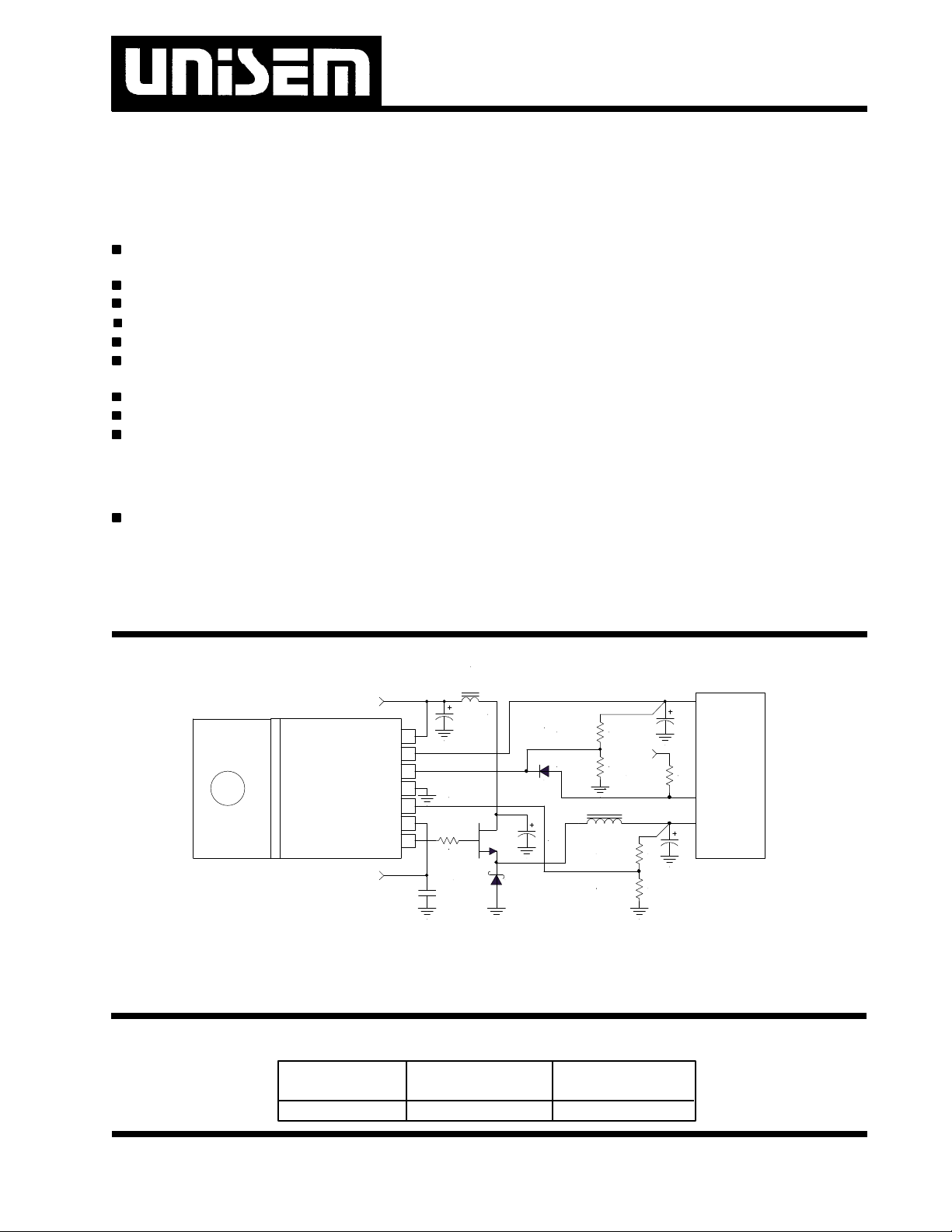
TYPICAL APPLICATIONTYPICAL APPLICATION
L1
I / O
C6
CPU
Vcc2 Det
Core
C7
2076app1-1.2
US2076
5V
12V
Vin
Vout
Vfb2
Gnd
Vfb1
V12
Drv
C1
7
6
5
4
3
2
R1
1
C3
C2
Q2
D1
R6
R7
D2
5V
R8
L2
R4
R5
Typical application of US2076 in a flexible motherboard designed for Intel
P55,P54, AMD K5 & K6 as well as Cyrix M1 and M2 applications.
Notes: P54C,P55C are trade marks of Intel Corp. K5 & K6 are trade marks of AMD corp. Cyrix 6X86L,M1,M2 are trade marks of Cyrix
Corp. Power PC is trade mark of IBM Corp.
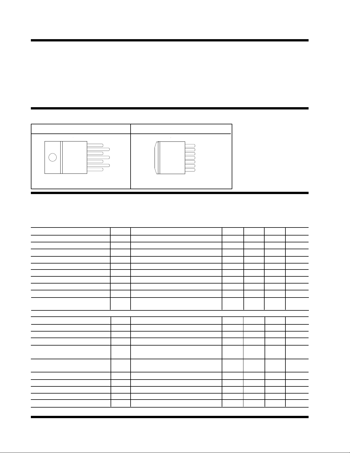
PACKAGE ORDER INFORMATIONPACKAGE ORDER INFORMATION
Tj (°C) 7 PIN PLASTIC 7 PIN PLASTIC
TO220 (T) TO263 (M)
0 TO 125 US2076CT US2076CM
Rev. 1.3
4/26/98
4-1
Page 2
US2076
ABSOLUTE MAXIMUM RATINGSABSOLUTE MAXIMUM RATINGS
12V Supply Voltage ............................................................. 14V
Vin Supply Voltage .............................................................. 7V
LDO Power Dissipation .................................... Internally Limited
FB Pin Voltage........................................................ -0.3V to 5V
Storage Temperature Range ................................. -65 TO 150°C
Operating Junction Temperature ............................... 0 TO 150°C
PACKAGE INFORMATIONPACKAGE INFORMATION
7 PIN PLASTIC TO220 (T) 7 PIN PLASTIC TO263 (M)
FRONT VIEW
7
6
5
4
3
2
1
Vin
Vfb2
Vfb1
Drv
Vout
Gnd
V12
FRONT VIEW
7
Vin
6
Vout
5
Vfb2
4
Gnd
3
Vfb1
2
V12
1
Drv
θJT=2.7°C/W θJA=60°C/W θJA=35°C/W for 1" Square pad
ELECTRICAL SPECIFICATIONSELECTRICAL SPECIFICATIONS
Unless otherwise specified the following specification applies over,Vin=5V,V12=12V,and Tj=0 to 125°C.Low duty
cycle pulse testing are used which keeps junction and case temperatures equal to the ambient temperature.
LDO Section
PARAMETER SYM TEST CONDITION MIN TYP MAX UNITS
F.B Voltage Initial Accuracy Vfb2 Tj=25°C 1.237 1.250 1.262 V
F.B Voltage Total Variation Vfb2 1.225 1.250 1.275 V
F.B Input Bias Current Ifb2 Vfb2=1.25V -1 +1 uA
Dropout Voltage (note 2) Vout=1.25V, Io=7.5A 1.1 V
Line Regulation Vout=1.25V,Io=10mA, 3<Vin<6V 0.2 %
Load Regulation (note 1) Vout=1.25V, 10mA<Io<7.5A 0.5 %
Thermal Regulation 30 mS Pulse 0.01 %/W
Minimum Load Current (note 3) 10 mA
Ripple Rejection f=120HZ ,Co=25uF Tan,Io=1A 70 dB
V12 Supply Current Icc2 Vfb2=1V, Vfb1=1.5V, Io=7.5A 75 mA
Switching Controller Section
PARAMETER SYM TEST CONDITION MIN TYP MAX UNITS
F.B Voltage Initial Accuracy Vfb1 Tj=25°C 1.237 1.250 1.262 V
F.B Voltage Total Variation Vfb1 1.225 1.250 1.275 V
F.B Input Bias Current Ifb1 Vfb1=1.25V -1 +1 uA
Min On Time Vfb1 is sq wave with 300 ns on 800 nS
time and 2 uS off time
Min Off Time Vfb1 is sq wave with 300 ns off 800 nS
time and 2 uS on time
V12 Supply Current Icc1 Vfb1=1V, Vfb2=1.5V 10 mA
Maximum Duty Cycle Dmax Vfb1=1V 100 %
Minimum Duty Cycle Dmin Vfb1=1.5V 0 %
Gate Drive Rise/Fall Time Vgate Load=IRL3303 70 nS
F.B Hysterises 12 mV
4-2
Rev. 1.3
4/26/98
Page 3

US2076
Note 1 : Low duty cycle pulse testing with Kelvin con-
nections are required in order to maintain accurate data.
Note 2 : Drop-out voltage is defined as the minimum
differential voltage between Vin and Vout required to maintain regulation at Vout. It is measured when the output
voltage drops 1% below its nominal value.
Note 3 : Minimum load current is defined as the minimum current required at the output in order for the output voltage to maintain regulation. Typically the resistor
dividers are selected such that it automatically maintains this current.
PIN DESCRIPTIONSPIN DESCRIPTIONS
PIN # PIN SYMBOL PIN DESCRIPTION
3 Vfb1 A resistor divider from this pin to the output of the switching regulator and
ground sets the Core supply voltage.
6 Vout The output of the linear regulator. A minimum of a 100uF low ESR capacitor must be
connected from this pin to ground to insure stability.
7 Vin The input pin of the linear regulator. Typically a large storage capacitor is connected
from this pin to ground to insure that the input voltage does not sag below the minimum
drop out voltage during the load transient response. This pin must always be higher than
Vout plus the maximum dropout voltage in order for the device to regulate properly.
4 Gnd This pin is connected to the IC substrate and must be connected to the lowest
potential in the system. It is also connected to the Tab of the package.
1 Drv The PWM output of the switching controller. This pin is a totem pole drive that is
connected to the gate of the power MOSFET. A resistor may be placed in series from
this pin to the gate in order to reduce switching noise.
5 Vfb2 A resistor divider from this pin to the output of the linear regulator and
ground sets the I/O supply voltage.
2 V12 This pin is connected to the 12V supply voltage. A high frequency cap must be
connected from this pin to the GND pin of the IC.
BLOCK DIAGRAMBLOCK DIAGRAM
V12 Vout
2 3 67
Drv
1
Gnd
4
Rev. 1.3
4/26/98
Vfb 1 Vin
UVLO
Vref
PWM Control
2076blk1-1.1
Figure 1 - Simplified block diagram of the US2076
1.25V
5V Reg
Vfb2
5
4-3
Page 4

US2076
TYPICAL APPLICATIONTYPICAL APPLICATION
5V
Vout
Vfb2
U1
2076app2-1.2
Gnd
Vfb1
V12
12V
Vin
Drv
7
6
5
4
3
2
1
C3
L1
C1
R6
R7
D2
L2
R1
C4
R2
C2
Q2
R5A R5B R5C R5D R5E
D1
JP1
1
2345678
R4A
5V
R8
R4B
I / O
C6
CPU
Vcc2 Det
Core
C7
Figure2- Typical application of US2076 in a flexible motherboard with the 4 bit VID output voltage selection. This circuit
uses a single jumper that programs the output voltage in 16 steps with 0.1V steps from 2V to 3.5V, designed for Intel P55,P54,
AMD K5 & K6 as well as Cyrix M1 and M2 applications. The Vcc2Det pin automatically shuts down the I/O when a single plane
processor is dropped in the socket.
Ref Desig Description Qty Part # Manufacturer
U1 LDO/Switcher IC 1 US2076CT (TO220) Unisem
US2076CM (TO263) (note 1)
Q1 MOSFET 1 IRL3303 (TO220) International
IRL3103S (TO263) (note 1) Rectifier
D1 Schottky Diode 1 MBR1045CT (TO220) Motorola
MBRB1545CT (TO263) (note1)
D2 Diode, GP 1 1N4148
L2 Inductor 1 Core:T50-18,L=4 uH Micro Metal
Turns: 10T, 18 AWG (core)
L1 Inductor 1 L=2 uH
R1 Resistor 1 22 ohm,5%, SMT 1206 size
R2 Resistor 1 10 ohm, 5%, SMT 1206 size
R4A Resistor 1 806 ohm,1%, SMT 0805 size
R4B Resistor 1 90.9 kohm,1%, SMT 0805 size
R5A Resistor 1 1.24 kohm,1%, SMT 0805 size
R5B Resistor 1 2.49 kohm,1%, SMT 0805 size
R5C Resistor 1 4.99 kohm,1%, SMT 0805 size
R5D Resistor 1 10 kohm,1%, SMT 0805 size
R5E Resistor 1 1.30 kohm,1%, SMT 0805 size
R6 Resistor 1 ohm,1%, SMT 0805 size
R7 Resistor 1 ohm,1%, SMT 0805 size
R8 Resistor 1 10 kohm,5%, SMT 0805 size
C3 Capacitor 1 1 uF,Ceramic, SMT 0805 size, Z5U
C1 Capacitor 1 EEUFA1A681L, 680uF,10V, Elect Panasonic
C4 Capacitor 1 470pF,Ceramic, SMT 0805 size
C2 Capacitor 1 6MV1500GX, 1500uF,6.3V, Elect Sanyo
C6 Capacitor 1 EEUFA1A681L, 680uF,10V, Elect Panasonic
C7 Capacitor 4 6MV1500GX, 1500uF,6.3V, Elect Sanyo
HS1 Heat Sink 1 For MOSFET , 577002 Aavid
HS2 Heat Sink 1 For Schottky Diode , 577002 Aavid
HS3 Heat Sink 1 For US2076 , 507222 (I/O Load Current<5A) Aavid
576602 (I/O Load Current< 3.5A)
Note 1: For the applications where it is desirable to eliminate the heat sink, the US2076CM for U1 when load current is
less than 1.5A, the IRL3103S for Q2 and MBR1545CT for D1 in TO263 packages with minimum of 1" square copper pad
can be used.
4-4
Rev. 1.3
4/26/98
 Loading...