

Page 1
US3033
PWM SWITCHER & LINEAR
CONTROLLER IC
FEATURESFEATURES
LDO Controller allows the use of a low cost
pass transistor for the I/O supply
8 pin SOIC combines switching and linear
controller
Internal Pre-regulator Eliminates Cross talk
between Switching & Linear regulators
Automatic shut down of the linear regulator
when connected to the Vcc2 Det pin
On board MOSFET driver
Fastest transient response of any controller
method. ( 0 to 100% Duty Cycle in 100 nS )
1% internal voltage reference
Internal Under Voltage Lockout protects
MOSFET during start-up
APPLICATIONSAPPLICATIONS
Dual supply low voltage processor applications,
such as: P55C,CYRIX M2, POWER PC and
AMD K6
Simple 5V to 3.3V switcher for Pentium with AGP
or Pentium II applications
DESCRIPTIONDESCRIPTION
The US3033 IC combines a switching controller and
a linear regulator controller all in a compact 8 pin
surface mount package, providing a total solution for
dual supply processor applications such as an Intel
P55C , AMD K6, as well as Cyrix 6X86L and
the M2processors. Typically in these applications a
dual supply regulator converts 5V to 3.3V for I/O supply
and a jumper programmable supply of 1.25V to 3.5V for
CORE supply .The linear regulator controller portion in
the US3033 is a programmable controller allowing flexibility for the I/O regulator and has a minimum of 50mA
drive current capability designed to provide ample current for an external pass transistor. The IC uses an internal regulator generated from the 12V supply to power
the controller as well as the 12V supply to drive the power
MOSFET, allowing a low cost N channel MOSFET
switch to be used. The IC also includes an error comparator for fast transient response, a precise voltage reference for setting the output voltage as well as a direct
drive of the MOSFET for the minimum part count.
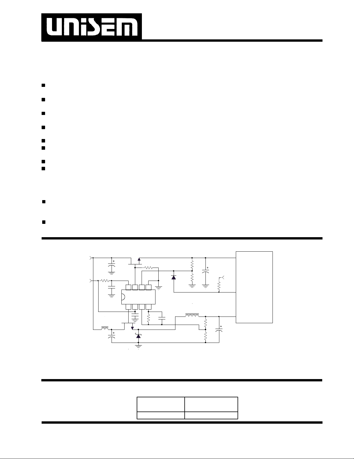
TYPICAL APPLICATIONTYPICAL APPLICATION
C1
C8
Drv1V12swVfb1Vhyst
1 2 3 4
C3
Q2
Q1
US3033
R10
5678
GndVfb2Drv2V12
D1C2
R3 C5
R6
C6
D2
R7
L2
R4
R5
5V
R9
12V
L1
Typical application of US3033 in a flexible mother board designed for Intel P55,P54
AMD K5,K6 as well as Cyrix M1 and M2 applications.
Notes: P54C,P55C,Pentium II are trade marks of Intel Corp. K5 & K6 are trade marks of AMD corp. Cyrix 6X86L,M1,M2 are trade marks
of Cyrix Corp. Power PC is trade mark of IBM Corp.
I / O
5V
R8
C7
CPU
Vcc2 Det
Core
3033app1-1.1
PACKAGE ORDER INFORMATIONPACKAGE ORDER INFORMATION
TA (°C) 8 PIN PLASTIC
SOIC (S)
0 TO 70 US3033CS
Rev. 1.5
1/14/99
4-1
Page 2
US3033
ABSOLUTE MAXIMUM RATINGSABSOLUTE MAXIMUM RATINGS
V12,V12SW Supply Voltages ............................................................. 20V
F.B Pin Voltages........................................................ -0.3V to 5V
Storage Temperature Range ................................. -65 TO 150°C
Operating Junction Temperature ............................... 0 TO 150°C
PACKAGE INFORMATIONPACKAGE INFORMATION
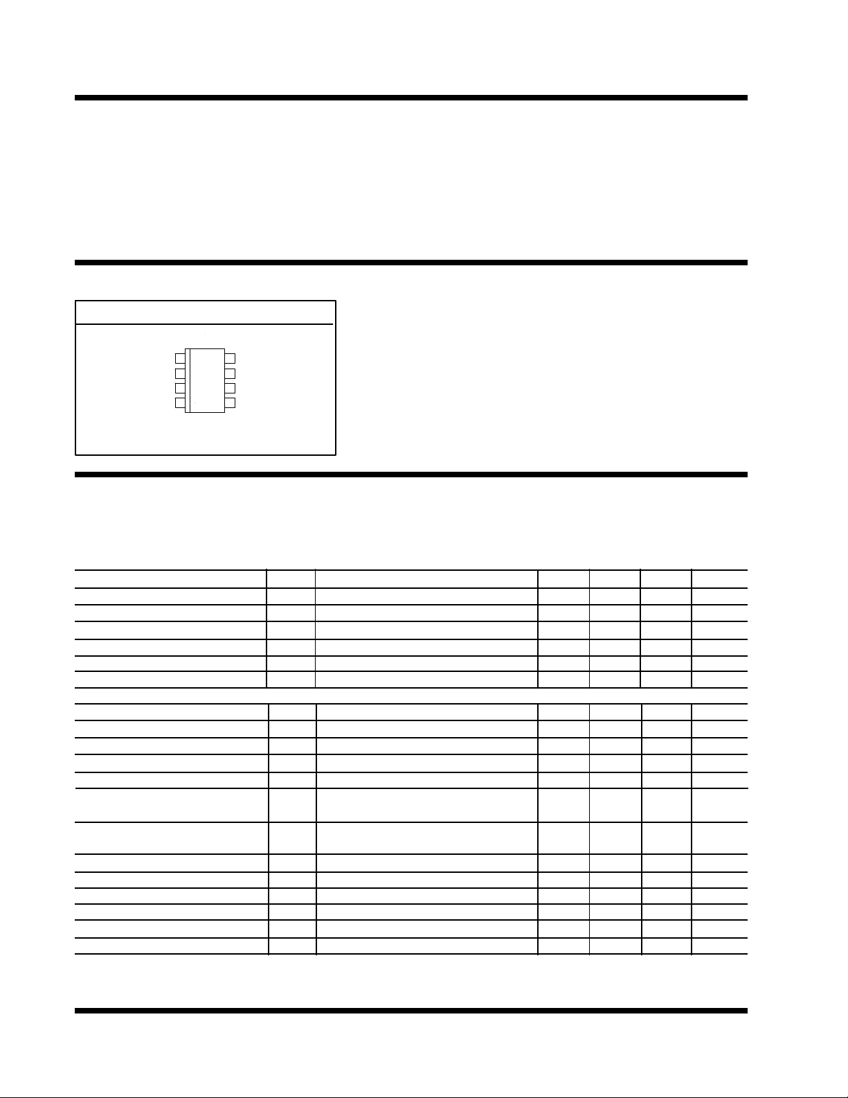
8 PIN PLASTIC SOIC (S)
TOP VIEW
1
Drv1
2
V12sw
3
Vfb1
4
Vhyst Gnd
θJA =160°C/W
8
V12
7
Drv2
6
Vfb2
5
ELECTRICAL SPECIFICATIONSELECTRICAL SPECIFICATIONS
Unless otherwise specified the following specification applies over V12 =V12SW =12V, and TA =0 to 70°C. Low duty
cycle pulse testing are used which keeps junction and case temperatures equal to the ambient temperature.
Linear Controller Section
PARAMETER SYM TEST CONDITION MIN TYP MAX UNITS
F.B Voltage Initial Accuracy VFB2 TJ =25°C, Drv2=VFB2, CL=100uF 1.237 1.250 1.262 V
F.B Voltage Total Variation Drv2=VFB2, CL=100uF 1.225 1.250 1.275 V
F.B Voltage Line Regulation 10<V12<14V,Drv2=VFB2, CL=100uF 0.2 %
F.B Input Bias Current IFB2 VFB2 =1.25V -1 +1 uA
Maximum Drive Current IDRVMAX VFB2 =1V, VFB1 =1.5V 50 mA
V12 Supply Current I12 VFB2 =1V, VFB1 =1.5V, IDRV2 =0 5 mA
Switching Controller Section
PARAMETER SYM TEST CONDITION MIN TYP MAX UNITS
F.B Voltage Initial Accuracy VFB1 TJ =25°C 1.237 1.250 1.262 V
F.B Voltage Total Variation 1.225 1.250 1.275 V
F.B Voltage Line Regulation 0.2 %
F.B Input Bias Current IFB1 VFB1 =1.25V -1 +1 uA
Min On Time VFB1 is sq wave with 300 ns on 800 nS
time and 2 uS off time
Min Off Time VFB1 is sq wave with 300 ns off 800 nS
time and 2 uS on time
Vhyst pin output-HI ISOURCE =500uA, VFB1 =1.5V 11 V
Vhyst pin output-LO ISINK =500uA, VFB1 =1V 1 V
Supply Current I12SW VFB1 =1V , VFB2 =1.5V 10 mA
Maximum Duty Cycle DMAX VFB1 =1V 100 %
Minimum Duty Cycle DMIN VFB1 =1.5V 0 %
Gate Drive Rise/Fall Time VGATE Load=IRL3303 70 nS
4-2
Rev. 1.5
1/14/99
Page 3
PIN DESCRIPTIONSPIN DESCRIPTIONS
PIN # PIN SYMBOL PIN DESCRIPTION
3 VFB1
6 VFB2
7 Drv2
5 Gnd
1 Drv1
4 VHYST
2 V12SW
8 V12
A resistor divider from this pin to the output of the switching regulator and ground sets the
Core supply voltage.
The feedback pin of the linear regulator. A resistor divider from this pin to the output of the
linear regulator and ground sets the I/O supply voltage.
The drive pin of the linear regulator. This pin controls the base of a transistor or the gate
of a MOSFET acting as the series pass element for the linear regulator.
This pin is connected to the IC substrate and must be connected to the lowest potential
in the system.
The PWM output of the switching controller. This pin is a totem pole drive that is connected to the gate of the power MOSFET. A resistor may be placed from this pin to the
gate in order to reduce switching noise.
A resistor and a 10pF capacitor is connected from this pin to the VFB1 pin to set the
output ripple voltage for the switching regulator.
This pin supplies the voltage to the PWM drive and hysterises circuitry and it is connected to the 12V supply. A 1 uF, high frequency capacitor must be connected from this
pin to ground to provide the peak current for charging and discharging of the MOSFET.
This pin provides the biasing for the chip and drive for the linear regulator controller. It
isconnected to 12V supply. A 10 ohm resistor in series from this pin to the 12V supply
and a 1uF, high frequency capacitor connected from this pin to Gnd is required to filter
the switching noise of the switching regulator.
US3033
BLOCK DIAGRAMBLOCK DIAGRAM
V12sw Vhyst
2 4 3
Drv 1
1
Gnd
5
Vfb 1
UVLO
Vref
PWM Control
3033blk1-1.0
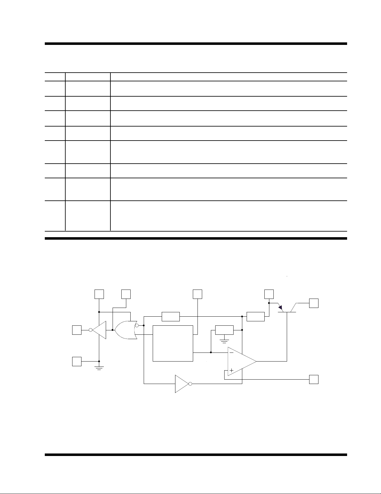
Figure 1 - Simplified block diagram of the US3033
1.25V
5V Reg
V12
8
Drv 2
7
Vfb2
6
Rev. 1.5
1/14/99
4-3
Page 4
US3033
TYPICAL APPLICATIONTYPICAL APPLICATION
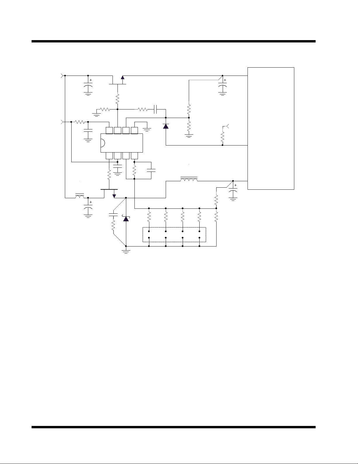
Pentium Dual Supply Application
5V
12V
R9
L1
C1
R10
C8
Drv1V12swVfb1 Vhyst
1 2 3 4
C3
R1
Q2
C2
C4
Q1
U1
D1R2
R11
GndVfb2Drv2V12
5678
JP1
C9
R13
D2
R3 C5
R5A R5B R5C R5D R5E
1
3
5
2
4
6
L2
R6
R7
I / O
C6
CPU
5V
R8
Vcc2 Det
Core
C7
R4
7
8
3033app2-1.3
Figure2- Typical application of US3033 in a flexible motherboard with the 4 bit VID output voltage selection. This circuit uses
a single jumper that programs the output voltage in 16 steps with 0.1V steps from 2V to 3.5V, designed for Intel P55,P54, AMD K5
& K6 as well as Cyrix M1 and M2 applications. The Vcc2Det pin automatically shuts down the I/O regulator when a single plane
processor is dropped in the socket.
JP1 JP1 JP1 JP1 Output
1-2 3-4 5-6 7-8 Voltage
0 0 0 0 3.5
0 0 0 1 3.4
0 0 1 0 3.3
0 0 1 1 3.2
0 1 0 0 3.1
0 1 0 1 3.0
0 = Jumper block is installed.
1 = Jumper block is not installed.
0 1 1 0 2.9
0 1 1 1 2.8
1 0 0 0 2.7
1 0 0 1 2.6
1 0 1 0 2.5
1 0 1 1 2.4
1 1 0 0 2.3
1 1 0 1 2.2
1 1 1 0 2.1
1 1 1 1 2.0
4-4
Rev. 1.5
1/14/99
Page 5
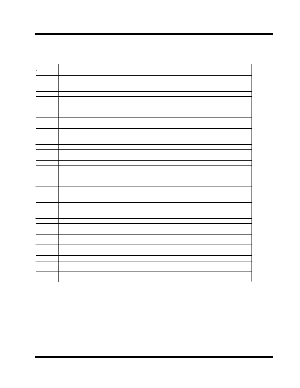
Pentium Dual Supply Application Parts List
Ref Desig Description Qty Part # Manufacturer
U1 LDO/Switcher IC 1 US3033CS ( 8 pin SOIC) Unisem
Q1 MOSFET 1 MTP3055 (TO220) Motorola
Q2 MOSFET 1 IRL3303 (TO220) International
IRL3103S (TO263) (note 1) Rectifier
D2 Diode, GP 1 1N4148
D1 Schottky Diode 1 MBR1045CT (TO220)
MBRB1545CT (TO263) (note1) Motorola
L2 Inductor 1 Core:T50-18,L=4 uH Micro Metal
Turns: 10T, 18 AWG (core)
L1 Inductor 1 L=2 uH
R1 Resistor 1 22 ohm,5%, SMT 1206 size
R2 Resistor 1 10 ohm, 5%, SMT 1206 size
R3 Resistor 1 324 kohm,1%, SMT 0805 size
R4A * Resistor 1 806 ohm,1%, SMT 0805 size
R4B * Resistor 1 90.9 kohm,1%, SMT 0805 size
R5A Resistor 1 1.24 kohm,1%, SMT 0805 size
R5B Resistor 1 2.49 kohm,1%, SMT 0805 size
R5C Resistor 1 4.99 kohm,1%, SMT 0805 size
R5D Resistor 1 10 kohm,1%, SMT 0805 size
R5E Resistor 1 1.30 kohm,1%, SMT 0805 size
R6 Resistor 1 2k ohm,1%, SMT 0805 size
R7 Resistor 1 1.21k ohm,1%, SMT 0805 size
R8 Resistor 1 1 kohm,5%, SMT 0805 size
R9 Resistor 1 10 ohm,5%, SMT 0805 size
R10 Resistor 1 1k ohm,5%, SMT 0805 size
R11 Resistor 1 2.4k ohm,5%, SMT 0805 size
R13 Resistor 1 7.5k ohm,5%, SMT 0805 size
C1 Capacitor 1 6MV1500GX, 1500uF,6.3V, Elect
C2 Capacitor 1 6MV1500GX, 1500uF,6.3V, Elect Sanyo
C3 Capacitor 1 1 uF,Ceramic, SMT 0805 size
C4 Capacitor 1 470 pF,Ceramic, SMT 0805 size Sanyo
C5 Capacitor 1 10 pF,Ceramic, SMT 0805 size Sanyo
C6 Capacitor 1 6MV1500GX, 1500uF,6.3V, Elect Sanyo
C7 Capacitor 4 6MV1500GX, 1500uF,6.3V, Elect Sanyo
C8 Capacitor 1 1 uF,Ceramic, SMT 0805 size
C9 Capacitor 1 470pF ,Ceramic, SMT 0805 size
HS1 Heat Sink 1 For MOSFET , 577002 Aavid
HS2 Heat Sink 1 For Schottky Diode , 577002 Aavid
HS3 Heat Sink 1 For Q1 , 507222 (I/O curren<5A) Aavid
576602 (I/O current< 3.5A)
US3033
* R4 is a parallel combination of R4A and R4B.
Note 1: For the applications where it is desirable to eliminate the heat sink, the IRL3103S for Q2 and MBR1545CT for D2 in TO263
packages with minimum of 1" square copper pad can be used.
Rev. 1.5
1/14/99
4-5
Page 6
US3033
TYPICAL APPLICATIONTYPICAL APPLICATION
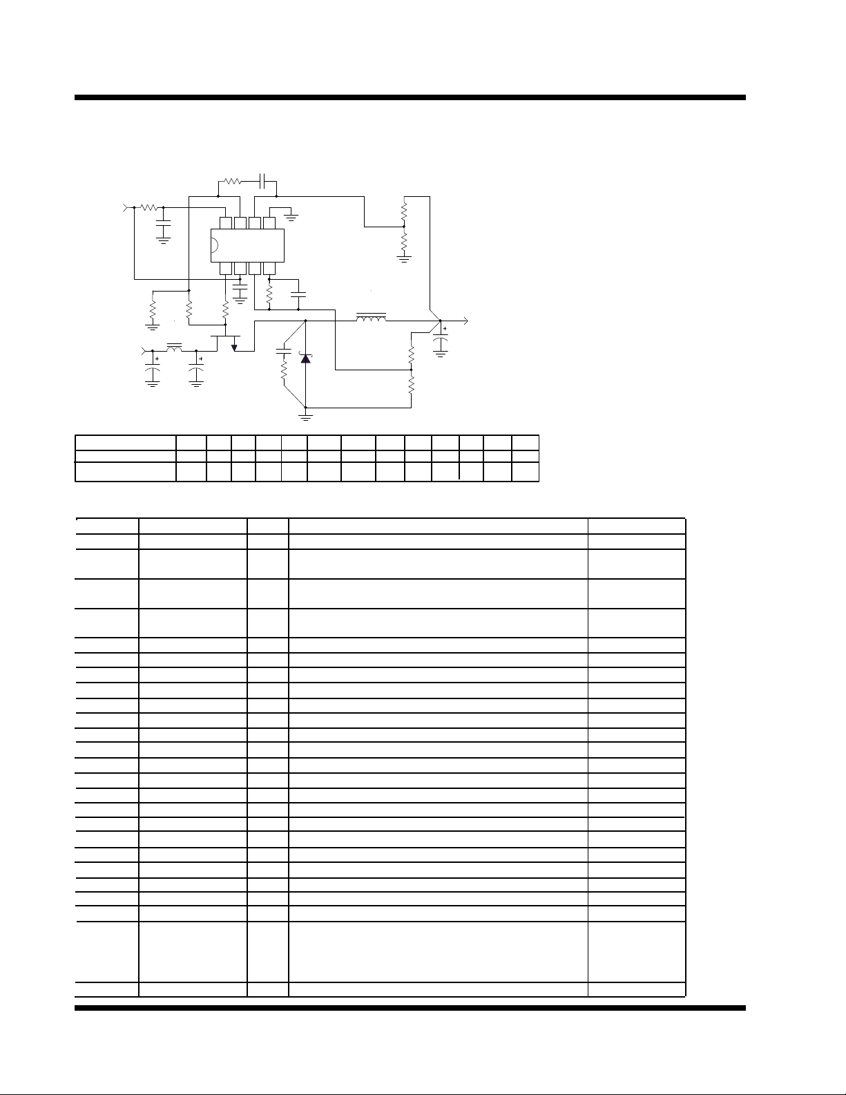
5V to 3.3V for Pentium Application with AGP or Pentium II Application without ATX power supply
Dual mode Operation between Switching or Linear mode.
5V
R10
R9
C8
R1A R1B
L1
C1
C3
C2
12V
Mode of Operation L1 L2 D1 C4 C5 R1A R1B R2 R3 R4 R5 R6 R7
Switching V V V V V O V V V V V V O
Linear S S O O O V O O O V O V V
C9
R13
GndVfb2Drv2V12
U1
Drv1V12swVfb1Vhyst
1 2 3 4
Q2
C4
5678
R3 C5
Figure3- This unique application of US3033 allows the de-
signer to switch between Linear or Switching mode of
R6
R7
L2
R4
D1R2
R5
3033app3-1.3
operation using a single IC. This circuit has the flexibility
to be used for low current operation in Linear mode for
cost reasons and yet be able to operate in the Switching
mode if the load current increases and the heat generated by the Linear operation will be an issue. Table below
descibes the components that will be effected for the
two modes of operation.
Vout
C7
Note 1: For the applications where it is desirable to
eliminate the heat sink, the IRL3103S for Q2 and
MBR1545CT for D2 in TO263 packages with minimum of
1" square copper pad can be used.
V = See parts list for value S = Short O = Open
Ref Desig Description Qty Part # Manufacturer
U1 LDO/Switcher IC 1 US3033CS ( 8 pin SOIC) Unisem
Q2 MOSFET 1 IRL3303 (TO220) International
IRL3103S (TO263) (note 1) Rectifier
D1 Schottky Diode 1 MBR1045CT (TO220)
MBRB1545CT (TO263) (note1) Motorola
L2 Inductor 1 Core:T50-18,L=4 uH Micro Metal
Turns: 10T, 18 AWG (core)
L1 Inductor 1 L=2 uH
R1A Resistor 1 2.4k ohm,5%, SMT 1206 size
R1B Resistor 1 22 ohm,5%, SMT 1206 size
R2 Resistor 1 10 ohm, 5%, SMT 1206 size
R3 Resistor 1 249 kohm,1%, SMT 0805 size
R4 Resistor 1 1 kohm,1%, SMT 0805 size
R5 Resistor 1 576 ohm,1%, SMT 0805 size
R6 Resistor 1 180 ohm,1%, SMT 0805 size
R7 Resistor 1 100 ohm,1%, SMT 0805 size
R9 Resistor 1 10 ohm, 5%, SMT 1206 size
R10 Resistor 1 1k ohm, 5%, SMT 1206 size
R13 Resistor 1 7.5k ohm, 5%, SMT 1206 size
C1,2 Capacitor 2 6MV1500GX, 1500uF,6.3V, Elect Sanyo
C3 Capacitor 1 1 uF,Ceramic, SMT 0805 size
C4 Capacitor 1 470 pF,Ceramic, SMT 0805 size Sanyo
C5 Capacitor 1 10 pF,Ceramic, SMT 0805 size Sanyo
C7 Capacitor 1 6MV1500GX, 1500uF,6.3V, Elect Sanyo
C8 Capacitor 1 1 uF,Ceramic, SMT 0805 size
C9 Capacitor 1 470pF,Ceramic, SMT 0805 size
HS1 Heat Sink 1 For MOSFET in Switching mode , 577002 Aavid
For MOSFET in Linear mode :
507222 (3.3V current<5A),
576602 (3.3V current< 3.5A)
HS2 Heat Sink 1 For Schottky Diode , 577002 Aavid
4-6
Rev. 1.5
1/14/99
Page 7
US3033
TYPICAL APPLICATIONTYPICAL APPLICATION
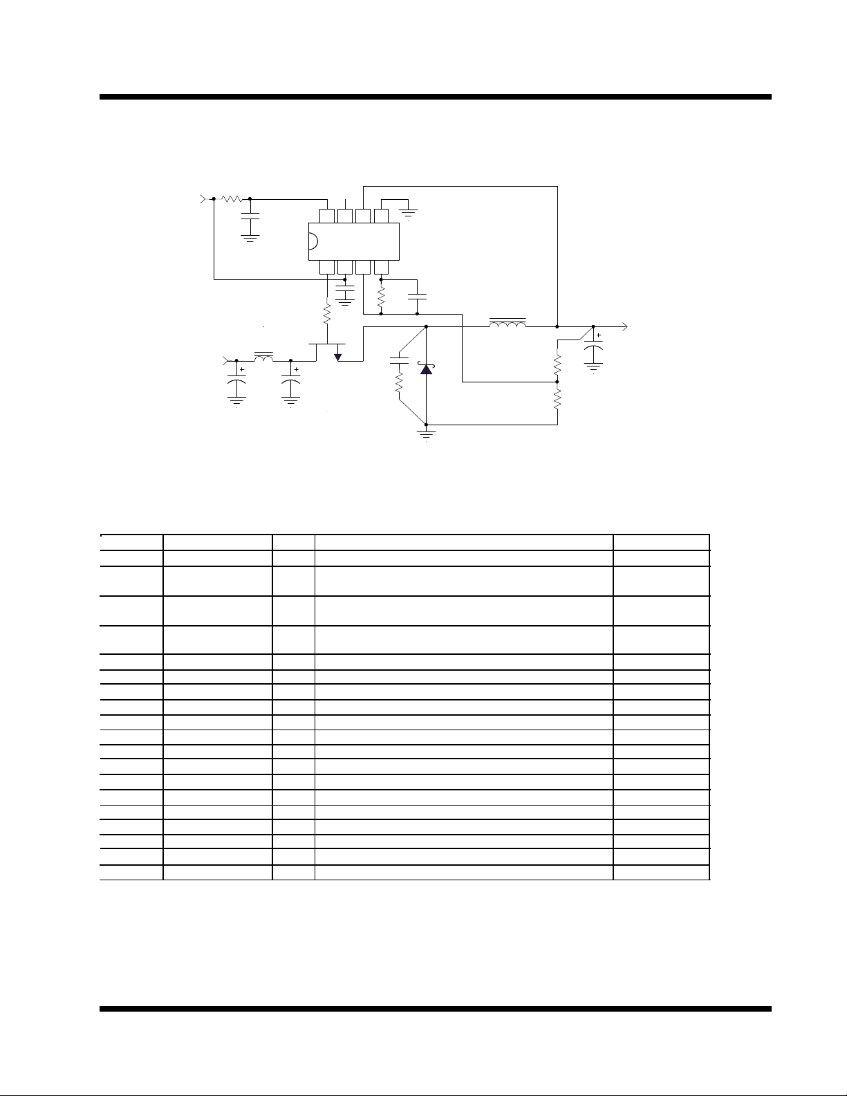
5V to 3.3V for Pentium Application with AGP or Pentium II Application without ATX power supply
Switching mode Operation.
12V
generate a low cost 5V to 3.3V for either Pentium application with AGP socket or in Pentium II applications where it is desirable to
generate an accurate on board 3.3V supply.
R9
C8
Drv1V12swVfb1Vhyst
1 2 3 4
C3
R1
L1
5V
C1
Figure4- The circuit in figure 4 is the application of the US3033 in a switching mode only. This circuit can be used to
Q2
C2
U1
5678
GndVfb2Drv2V12
R3 C5
C4
L2
Vout
C7
R4
D1R2
R5
3033app4-1.2
Ref Desig Description Qty Part # Manufacturer
U1 LDO/Switcher IC 1 US3033CS ( 8 pin SOIC) Unisem
Q2 MOSFET 1 IRL3303 (TO220) International
IRL3103S (TO263) (note 1) Rectifier
D1 Schottky Diode 1 MBR1045CT (TO220)
MBRB1545CT (TO263) (note1) Motorola
L2 Inductor 1 Core:T50-18,L=4 uH Micro Metal
Turns: 10T, 18 AWG (core)
L1 Inductor 1 L=2 uH
R1 Resistor 1 22 ohm,5%, SMT 1206 size
R9 Resistor 1 10 ohm,5%, SMT 0805 size
R2 Resistor 1 10 ohm, 5%, SMT 1206 size
R3 Resistor 1 249 kohm,1%, SMT 0805 size
R4 Resistor 1 1 kohm,1%, SMT 0805 size
R5 Resistor 1 576 ohm,1%, SMT 0805 size
C1,2 Capacitor 2 6MV1500GX, 1500uF,6.3V, Elect Sanyo
C3 Capacitor 1 1 uF,Ceramic, SMT 0805 size
C4 Capacitor 1 470 pF,Ceramic, SMT 0805 size Sanyo
C5 Capacitor 1 10 pF,Ceramic, SMT 0805 size Sanyo
C7 Capacitor 1 6MV1500GX, 1500uF,6.3V, Elect Sanyo
C8 Capacitor 1 1 uF,Ceramic, SMT 0805 size
HS1 Heat Sink 1 For MOSFET , 577002 Aavid
HS2 Heat Sink 1 For Schottky Diode , 577002 Aavid
Note 1: For the applications where it is desirable to eliminate the heat sink, the IRL3103S for Q2 and MBR1545CT for D2 in TO263
packages with minimum of 1" square copper pad can be used.
Rev. 1.5
1/14/99
4-7
Page 8

US3033
APPLICATION INFORMATIONAPPLICATION INFORMATION
Introduction
The US3033 device is an application specific product
designed to provide an on board dual supply for the new
generation of microprocessors requiring separate Core
and I/O supplies. One of the processors fitting this requirement is the new Intel P55C multimedia microprocessor. Intel specifies a Core voltage of 2.8V nominal
(±100mV max) with maximum Core supply current of
6A while the I/O supply is set for 3.3V with a maximum
I/O current of 0.65A. However in most applications the I/
O regulator also provides the voltage for other IC func-
tions such as the chip set ,Cache,....etc. Typically a
low cost solution such as a Low Dropout Linear Regulator (LDO) is selected to provide the I/O supply with the
maximum designed current of 3A , keeping the power
dissipation and the heat sink to a reasonable size. The
Core supply regulator however if also selected to be a
linear regulator , will be dissipating a maximum of 12.6W
((5V-2.8V)X5.7A) of power, which requires a substantial
amount of heat sinking and perhaps forced air cooling in
order to keep it operational. Some manufacturers suggest using two regulators to current share and therefore
distribute the power dissipation equally between the regulators. The problem is that , in order to equally current
share you need to sense both currents and force the
slave regulator to match the master regulator. This can
be done , but at the cost of the circuit complexity and
much higher system cost and the total power dissipation is still the same. In fact, if the task is to design a
flexible motherboard to accommodate the Cyrix 6X86L
or their future MMX processors as well, then the power
dissipation could easily reach 20W or more. At this power
dissipation level the choice for a switching regulator
approach becomes evident. However the main reason
that designers have always shied away from the switching regulators is their higher price tag and more complex circuit design that is associated with this kind of
technique.
The US3033 device is designed to take advantage
of the high efficiency of the switching regulator
technique for the Core supply while maintaining
the low cost LDO regulator for the I/O supply by
offering both control functions in a single 8 pin surface mount package. In fact as the typical application
circuit shows, one can design a complete flexible
motherboard using the US3033 and a few external components yielding a very low component count switching
regulator and with an addition of a low cost pass transis-
tor for the I/O supply provide a complete dual supply
power soloution.
LDO Section
The output voltage of the LDO regulator is externally programmable via 2 external resistors from 1.25V to 5V.
The internal voltage reference of the The LDO regulator
is set to 1.25V and the output of the regulator can be
programmed using the following formula:
Vout=(1+R1/R2)xVref
Where Vref=1.25V Typical
R1=Resistor connected from Vout to the Vfb2 pin of
US3033
R2=Resistor connected from Vfb2 pin to GND.
The US3033 requires the use of an output capacitor as
part of the frequency compensation in order to be stable.
Typical designs for the microprocessor applications use
standard electrolytic capacitors with typical ESR in the
range of 50 to 100 mΩ and an output capacitance of 500
to 1000uF. Fortunately as the capacitance increases,
the ESR decreases resulting in a fixed RC time constant. The US3033 takes advantage of this phenomena
in making the overall regulator loop stable. For most applications a minimum of 100uF aluminum electrolytic
capacitor such as Sanyo, MVGX series ,Panasonic FA
series or Nichicon PL series insures both stability and
good transient response.
An external filtering is suggested as shown in the application circuit that reduces the switching ripple that might
show in the output of the LDO regulator.
Switching Controller Operation
The operation of the switching controller is as follows :
after the power is applied, the output drive, "Drv1" goes
to 100% duty cycle and the the current in the inductor
charges the output capacitor causing the output voltage
to increase. When output reaches a pre-programmed
set point the feedback pin "Fb1" exceeds 1.25V causing the output drive to switch low and the "Vhyst" pin to
switch high which jumps the feedback pin higher than
1.25V resulting in a fixed output ripple which is given by
the following equation :
∆Vo=(Rt/Rh)x11
Where:
Rt=Top resistor of the output divider, resistor connected
from Vout to the Vfb1 pin of US3033
Rh=Bottom resistor of the divider, resistor connected from
Vfb1 pin to Vhyst pin.
For example, if Rt=1k and Rh=422k, then the output
ripple is :
∆Vo=(1/422)x11=26mV
4-8
Rev. 1.5
1/14/99
Page 9

The advantage of fixed output ripple is that when the
output voltage changes from 2V to 3.5V, the ripple voltage remains the same which is important in meeting the
Intel maximum tolerance specification.
Switcher Output Voltage Setting
The output voltage of the switcher can be set using the
following equations.
Assuming , Vo=3.38V and the selected output ripple is
≈ 1.3%(44mV) of the output voltage, a set of equations
are derived that selects the resistor divider and the
hysterises resistor.
Assuming, Rt=1kΩ , 1%
Rh=(11*Rt)/∆Vo
Where:
Rt=Top resistor of the resistor divider
Rh=Hysterises resistor connected between pins 3 and
4 of the US3033
∆Vo=Selected output ripple (typically 1% to 2% of output voltage)
Assuming, ∆Vo=44mV
Rh=(11*1000)/0.044=250 kΩ
Select Rh=249 kΩ , 1%
The bottom resistor of the divider is then calculated using the following equations:
Rb=Rt/X
Where:
Rb=Bottom resistor of the divider
X=[(Vo + (∆Vo/2))/Vref] - 1
Vref=1.25 V typ.
X=[(3.38+ (0.044/2))/1.25] - 1 = 1.72
Rb=1000/1.72=580 Ω
Select Rb=576 Ω , 1%
US3033
Frequency Calculation
The US3033 frequency of operation is calculated using
the following formula:
Fs=[(Vo*(1-D)*ESR)]/(L*∆Vo) (MHz)
Where:
Vo=Output voltage (V)
D=Duty cycle
ESR=Output capacitor ESR (V)
L=Output inductance (uH)
∆Vo=Output ripple voltage (V)
For our example:
D≈(Vo + Vf)/Vin
Where, Vf=Forward voltage drop of the Schotky diode
D=(3.38 + 0.5)/5=0.78
The ESR=18mΩ for 2 of the Sanyo 1500uF, 6MV1500GX
caps. If L=3.5uH then, Fs is calculated as follows:
Fs=[(3.38*(1-0.78)*0.018)]/(3.5*0.044)= 0.087 Mhz
= 87 kHz
Rev. 1.5
1/14/99
4-9
 Loading...