

Page 1

FEATURESFEATURES
8 pin SOIC Switching Controller with
HICCUP Current Limiting Reduces Diode Power
Dissipation to Less than 1% of Normal Operation
Soft Start Capacitor allows for smooth Output
Voltage ramp up
On board MOSFET driver
Fastest transient response of any controller
method. ( 0 to 100% Duty Cycle in 100 nS )
1% internal voltage reference
Internal Under Voltage Lockout protects
MOSFET during start-up
APPLICATIONSAPPLICATIONS
Single input Switching Regulators such as Simple
5V to 2.5V switcher for RDRAM regulator
US3036
8 PIN PWM SWITCHER
CONTROLLER IC
PRELIMINARY DATASHEET
DESCRIPTIONDESCRIPTION
The US3036 IC provides an 8 pin low cost switching
controller with true short circuit protection all in a
compact 8 pin surface mount package, providing a
low cost switching solution for applications that re-
quire a simple switching regulator from the 5V input where
there is no other supply available. One type of such
application is generating 2.5V standby from the dual
5V(5V and 5V standby) for the next generation processors. The IC starts below 4.5V supply and drives an
external Pch MOSFET or and external low cost PNP as
the switching element. The IC also includes an error comparator for fast transient response, a precise voltage reference for setting the output voltage as well as a direct
drive of the MOSFET for the minimum part count.
TYPICAL APPLICATIONTYPICAL APPLICATION
C8
ATX
P.S.
5V
5V(S.B.)
L1
C1
5678
GndCS-CS+SS
US3036
Drv Vcc Vfb NC
1 2 3 4
R1
C2
C3
Q2
C4
R3 C5
D1R2
Typical application of US3036
C6
R7
R6
L2
Vout
C7
R4
R5
3036app2-1.0
PACKAGE ORDER INFORMATIONPACKAGE ORDER INFORMATION
TA (°C) 8 PIN PLASTIC
SOIC (S)
0 TO 70 US3036CS
Rev. 1.1
12/4/98
4-1
Page 2
US3036
ABSOLUTE MAXIMUM RATINGSABSOLUTE MAXIMUM RATINGS
VCC Supply Voltage ............................................................. 20V
F.B Pin Voltage........................................................ -0.3V to 5V
Storage Temperature Range ................................. -65 TO 150°C
Operating Junction Temperature ............................... 0 TO 150°C
PACKAGE INFORMATIONPACKAGE INFORMATION
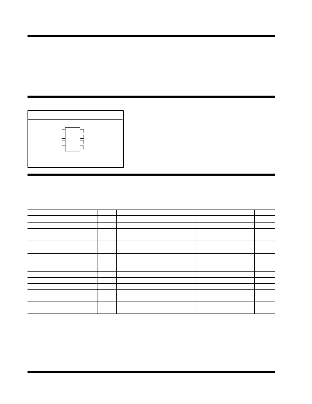
8 PIN PLASTIC SOIC (S)
TOP VIEW
1
Drv
2
Vcc
3
Vfb
4
NC Gnd
θJA =160°C/W
8
SS
7
CS+
6
CS-
5
ELECTRICAL SPECIFICATIONSELECTRICAL SPECIFICATIONS
Unless otherwise specified the following specification applies over VCC =5V, and TA =0 to 70°C. Low duty cycle
pulse testing are used which keeps junction and case temperatures equal to the ambient temperature.
PARAMETER SYM TEST CONDITION MIN TYP MAX UNITS
F.B Voltage Initial Accuracy VFB TJ =25°C 1.237 1.250 1.262 V
F.B Voltage Total Variation 1.225 1.250 1.275 V
F.B Voltage Line Regulation 0.2 %
F.B Input Bias Current IFB VFB =1.25V -1 +1 uA
Min On Time VFB is sq wave with 300 ns on 800 nS
time and 2 uS off time
Min Off Time VFB is sq wave with 300 ns off 800 nS
time and 2 uS on time
Supply Current ICCSW VFB =1.5V 10 mA
Maximum Duty Cycle DMAX VFB =1.5V 100 %
Minimum Duty Cycle DMIN VFB =1V 0 %
Gate Drive Rise/Fall Time VGATE Load=1000pF 70 nS
C.L Threshold Current ICL C.S+ , C.S- from 1.3V to 3.7V 20 uA
C.S Comp Common Mode VCS+ = VCS- 0 4.5 V
Soft Start Current 10 uA
UVLO Threshold VUVLO 4.25 4.4 4.55 V
4-2
Rev. 1.1
12/4/98
Page 3
PIN DESCRIPTIONSPIN DESCRIPTIONS
PIN # PIN SYMBOL PIN DESCRIPTION
3 VFB
6 C.S-
7 C.S+
5 Gnd
1 Drv
2 VCC
8 S.S
4 N.C
A resistor divider from this pin to the output of the switching regulator and ground sets the
Core supply voltage.
This pin is connected to the minus side of the external current sense resistor. An internal
current source together with an external resistor in series with this pin programs the
current limit threshold voltage. This voltage divided by the external current sense resistor
sets the current limit threshold.
This pin is connected to the plus side of the external current sense resistor. A resistor in
series with this pin and a capacitor connected between this pin and pin 6 provides a high
frequency filtering for the noise spikes of turn on and turn off switching.
This pin is connected to the IC substrate and must be connected to the lowest potential
in the system.
The PWM output of the switching controller. This pin is a totem pole drive that is connected to the gate of the power MOSFET. A resistor may be placed from this pin to the
gate in order to reduce switching noise.
This pin supplies the voltage to the PWM drive and hysterises circuitry and it is connected to the same supply as the input supply to the switching regulator . A 1 uF, high
frequency capacitor must be connected from this pin to ground to provide the peak current for charging and discharging of the MOSFET.
This pin provides the soft start for the regulator during power up. It also sets a long off
time when the converter goes into current limiting, providing low duty cycle for the catch
diode allowing it to survive during short circuit.
No connect.
US3036
BLOCK DIAGRAMBLOCK DIAGRAM
Vcc NC
2 4 3
Drv
1
Gnd
5
Vfb
5V Reg
UVLO
PWM Control
S.S. / Hiccup
Control
R
1.25V
R
20uA
Vref
3036blk1-1.2
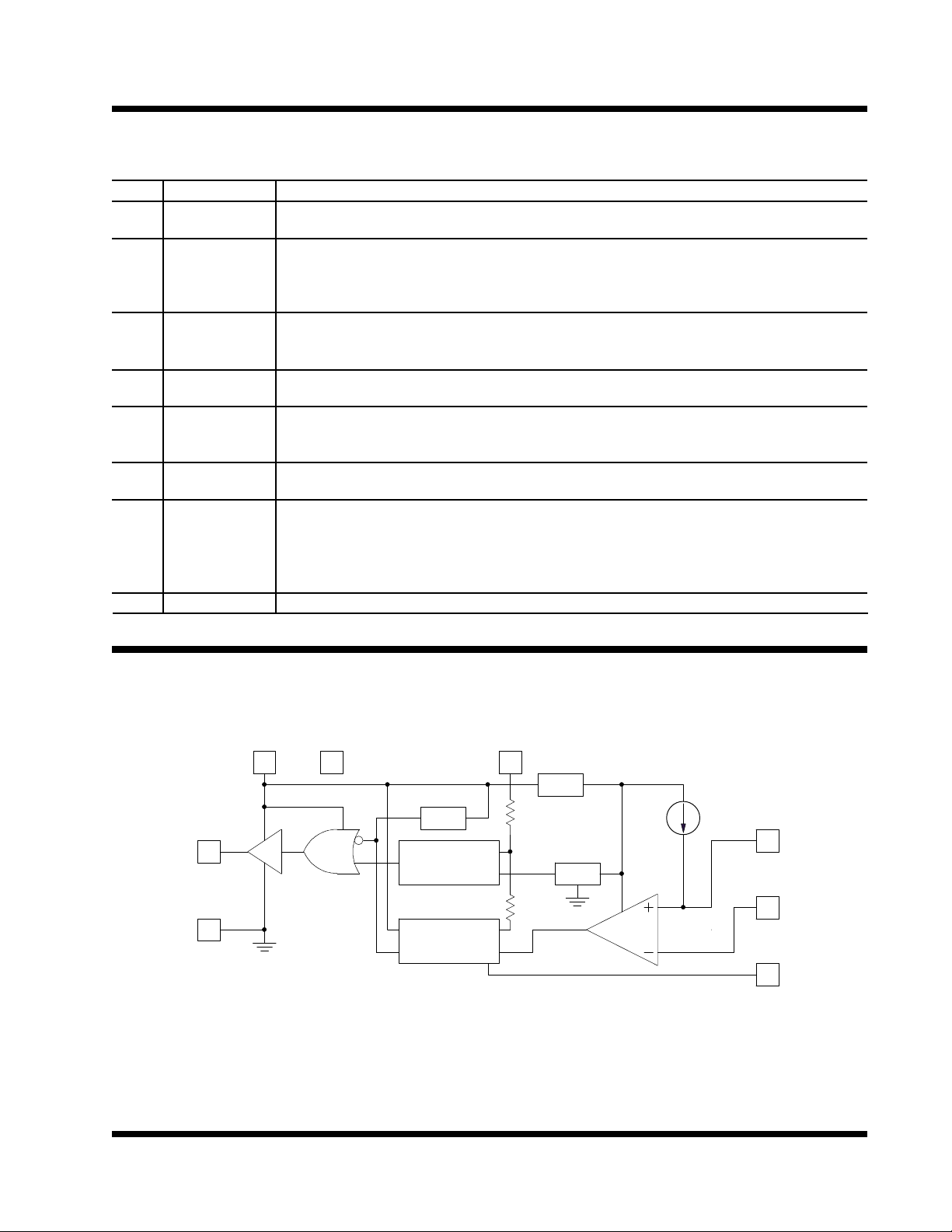
Figure 1 - Simplified block diagram of the US3036
CS-
6
CS+
7
SS
8
Rev. 1.1
12/4/98
4-3
Page 4
US3036
TYPICAL APPLICATIONTYPICAL APPLICATION
5V to 2.5V for RDRAM Supply
C8
5678
GndCS-CS+SS
C6
US3036
Drv Vcc Vfb NC
1 2 3 4
C3
R1
R3 C5
L2
R8
R7
R6
ATX
P.S.
5V
5V(S.B.)
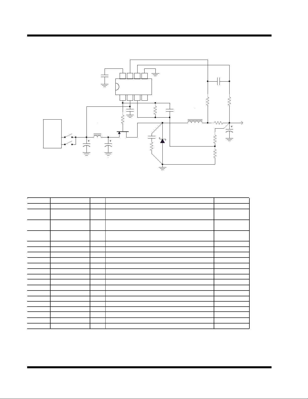
Figure 2- The circuit in figure 2 is the application of the US3036 providing a low cost solution for a 2.5V/2A supply from
the 5V dual supply. This circuit uses current sense resistor to set the current limiting.
C1
L1
C2
Q2
C4
R4
D1R2
R5
3036app1-1.3
Ref Desig Description Qty Part # Manufacturer
U1 LDO/Switcher IC 1 US3036CS ( 8 pin SOIC) Unisem
Q2 MOSFET 1 IRF7204 (8 pin SOIC) or IRF7406 for 4A IR
P Ch SI9435DY (8 pin SOIC) or SI4431 for 4A Temic
D1 Schottky Diode 1 SK33DICT (SMC) Lite on
C7
Vout
L2 Inductor 1 Core:T44-52,L=6 uH Micro Metal
Turns: 15T, 20 AWG (core)
L1 Inductor 1 L=1 uH
R1 Resistor 1 10 ohm,5%, SMT 1206 size
R2 Resistor 1 10 ohm, 5%, SMT 1206 size
R3 Resistor 1 200 kohm,1%, SMT 0805 size
R4 Resistor 1 1 kohm,1%, SMT 0805 size
R5 Resistor 1 1 kohm,1%, SMT 0805 size
R6 Resistor 1 5 miliohm,5%, 2W Ohmite
R7,8 Resistor 2 3.57 kohm,1%, SMT 0805 size
C1 Capacitor 1 470uF,10V, Elect Sanyo
C2 Capacitor 1 10CV1000DX, 1000uF,10V, Elect ,ESR=0.07 Ohm Sanyo
C3 Capacitor 1 1 uF,Ceramic, SMT 0805 size
C4 Capacitor 1 470 pF,Ceramic, SMT 0805 size Sanyo
C5 Capacitor 1 10 pF,Ceramic, SMT 0805 size Sanyo
C6 Capacitor 1 4700pF
C7 Capacitor 1 10CV1000DX, 1000uF,10V, Elect ,ESR=0.07 Ohm Sanyo
C8 Capacitor 1 0.15 uF
4-4
Rev. 1.1
12/4/98
Page 5
TYPICAL APPLICATIONTYPICAL APPLICATION
5V to 2.5V for RDRAM Supply
US3036
C8
5678
GndCS-CS+SS
US3036
Drv Vcc Vfb NC
1 2 3 4
C3
R1
R3 C5
C6
R7
R6
L2
ATX
P.S.
5V
5V(S.B.)
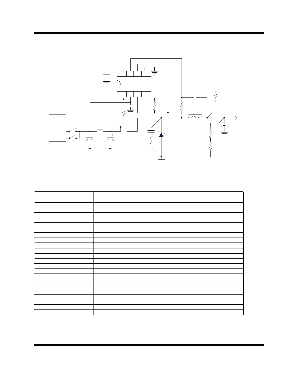
Figure 2- The circuit in figure 2 is the application of the US3036 providing a low cost solution for a 2.5V supply from
the 5V dual supply.
C1
L1
C2
Q2
C4
R4
D1R2
R5
3036app2-1.0
Ref Desig Description Qty Part # Manufacturer
U1 LDO/Switcher IC 1 US3036CS ( 8 pin SOIC) Unisem
Q2 MOSFET 1 IRF7204 (8 pin SOIC) or IRF7406 for 4A IR
P Ch SI9435DY (8 pin SOIC) or SI4431 for 4A Temic
D1 Schottky Diode 1 SK33DICT (SMC) Lite on
C7
Vout
L2 Inductor 1 Core:T44-52,L=6 uH Micro Metal
Turns: 15T, 20 AWG (core)
L1 Inductor 1 L=1 uH
R1 Resistor 1 10 ohm,5%, SMT 1206 size
R2 Resistor 1 10 ohm, 5%, SMT 1206 size
R3 Resistor 1 200 kohm,1%, SMT 0805 size
R4 Resistor 1 1 kohm,1%, SMT 0805 size
R5 Resistor 1 1 kohm,1%, SMT 0805 size
R6 Resistor 1 1 kohm,5%
R7 Resistor 1 3.57 kohm,1%, SMT 0805 size
C1 Capacitor 1 470uF,10V, Elect Sanyo
C2 Capacitor 1 10CV1000DX, 1000uF,10V, Elect ,ESR=0.07 Ohm Sanyo
C3 Capacitor 1 1 uF,Ceramic, SMT 0805 size
C4 Capacitor 1 470 pF,Ceramic, SMT 0805 size Sanyo
C5 Capacitor 1 10 pF,Ceramic, SMT 0805 size Sanyo
C6 Capacitor 1 0.1uF
C7 Capacitor 1 10CV1000DX, 1000uF,10V, Elect ,ESR=0.07 Ohm Sanyo
C8 Capacitor 1 0.15 uF
Rev. 1.1
12/4/98
4-5
Page 6

US3036
APPLICATION INFORMATIONAPPLICATION INFORMATION
Introduction
The US3036 device is an application specific product
designed to provide an on board switching supply for the
new generation of microprocessors requiring separate
Core and I/O supplies where the load current demand
from the I/O supply requires this regulator to also be a
switching regulator such as the motherboard applications with AGP slot or the Pentium II with on board 5V to
3.3V converter. The US3036 provides an easy and low
cost switching regulator solution for Vcore and 3.3V
supplies with true short circuit protection.
Switching Controller Operation
The operation of the switching controller is as follows :
after the power is applied, the output drive pin, "Drv" goes
low turning the P MOS to 100% duty cycle and the the
current in the inductor charges the output capacitor causing the output voltage to increase. When output reaches
a pre-programmed set point the feedback pin "Vfb" exceeds 1.25V causing the output drive to switch low and
the "Vhyst" pin to switch high which jumps the feedback pin higher than 1.25V resulting in a fixed output
ripple which is given by the following equation :
dVo=(Rt/Rh)x(Vcc -1)
Where:
Rt=Resistor connected from Vout to the Vfb pin of
US3036
Rh=Resistor connected from Vfb pin to Vhyst pin.
For example, if Rt=1k and Rh=200k, then the output
ripple is :
dVo=(1/200)x4=20 mV
The advantage of fixed output ripple method is that when
the output voltage changes from 2V to 3.5V, the ripple
voltage remains the same which is important in meeting
the Intel maximum tolerance specification.
Soft Start
The soft start capacitor must be selected such that during the start up when the output capacitors are charging
up, the peak inductor current does not reach the current
limit treshold. A minimum of 0.1uF capacitor insures
this for most applications. During start up the soft start
capacitor is charged up to approximately 6V keeping
the output shutdown before an internal 10uA current
source start discharging the soft start capacitor which
slowly ramps up the inverting input of the PWM comparator, Vfb. This insures the output to ramp up at the
same rate as the soft start cap thereby limiting the input
current. For example, with 0.1uF and the 10uA internal
current source the ramp up rate is (∆V/ ∆t)=I/Css = 10/
0.1=100V/Sec or 0.1V/mSec. Assuming that the output
capacitance is 6000uF, the peak input current will be:
Iin(pk)=Css*(∆V/ ∆t)=6000uF*(0.1V/mSec)=0.6A
The soft start capacitor also provides a delay in the turn
on of the output which is given by:
Td=CSS*K
Where K=30 ms/uF
For example for CSS=0.1uF,
Td=0.1* 30=3 ms
Switcher Current Limit Protection
The US3034 uses an external current sensing resistor
and compares the voltage drop across it to a programmed
voltage which is set externally via a resistor (RcL) placed
between the “CS-” terminal of the IC and Vout. Once the
voltage across the sense resistor exceeds the threshold, the soft start capacitor pulls up to 12V, pulling up
the inverting pin of the error comparator higher than non
inverting which causes the external MOSFET to shut
off. At this point the C.S comparator changes its state
and pulls the soft start capacitor to Vcc which is 12V
and shutting the PWM drive. After the output drive is
turned off, an internal 10uA current source slowly discharge the soft start capacitor to approximately 5.7V,
before the output starts to turn back on causing a long
delay before the MOSFET turns back on. This delay
causes the catch diode to cool off between the current
limit cycles allowing the converter to survive a short circuit condition. An example is given below as how to
select the current limiting components. Assuming the
desired current limit point is set to be 20A and the current sense resistor Rs=5mΩ, then the current limit pro-
gramming resistor,RcL is calculated as :
Vcs=IcL*Rs=20*0.005=0.1V
RcL=Vcs/Ib=(0.1V)/(20uA)=5kΩ
Where: Ib=20uA is the internal current source of the
US3034
The peak power dissipated in the C.S. resistor is :
Ppk=(IcL^2)*Rs=20^2*0.005=2W
However, the average power dissipated is much lower
than 2W due to the long off time caused by the hiccup
circuit of 3034. The average power is in fact the short
circuit period divided by the short circuit period plus the
off time or "hiccup" period. For example, if the short circuit lasts for TSC=100uSec before the 3034 enters hiccup, the average power is calculated as :
Pave=Ppk*DSC
Where:
DSC=TSC/THCP
THCP=CSS*M
Where M=630 ms/uF & CSS, is the soft start capacitor
For example for CSS=0.1uF & TSC=100uSec=0.1mS
THCP=0.1* 630=63 ms
Pave=2*(0.1/63)=3.2 mW
Without "hiccup" technique, the power dissipation
of the resistor is 2W.
4-6
Rev. 1.1
12/4/98
Page 7

Switcher Output Voltage Setting
The output voltage can be set using the following
equations.
Assuming , Vo=3.38V and the selected output ripple
is ≈ 1.3%(44mV) of the output voltage, a set of
equations are derived that selects the resistor divider
and the hysterises resistor.
Assuming, Rt=1kΩ , 1%
Rh=(11*Rt)/∆Vo
Where:
Rt=Top resistor of the resistor divider
Rh=Hysterises resistor connected between pins 3 and
4 of the US3034
∆Vo=Selected output ripple (typically 1% to 2% of
output voltage)
Assuming, ∆Vo=44mV
Rh=(11*1000)/0.044=250 kΩ
Select Rh=249 kΩ , 1%
The bottom resistor of the divider is then calculated
using the following equations:
Rb=Rt/X
Where:
Rb=Bottom resistor of the divider
X=[(Vo + (∆Vo/2))/Vref] - 1
Vref=1.25 V typ.
X=[(3.38+ (0.044/2))/1.25] - 1 = 1.72
Rb=1000/1.72=580 Ω
Select Rb=576 Ω , 1%
US3036
Frequency Calculation
The US3034 frequency of operation is calculated using
the following formula:
Fs=[(Vo*(1-D)*ESR)]/(L*∆Vo) (MHz)
Where:
Vo=Output voltage (V)
D=Duty cycle
ESR=Output capacitor ESR (V)
L=Output inductance (uH)
∆Vo=Output ripple voltage (V)
For our example:
D≈(Vo + Vf)/Vin
Where, Vf=Forward voltage drop of the Schotky diode
D=(3.38 + 0.5)/5=0.78
The ESR=18mΩ for 2 of the Sanyo 1500uF,
6MV1500GX caps. If L=3.5uH then, Fs is calculated
as follows:
Fs=[(3.38*(1-0.78)*0.018)]/(3.5*0.044)= 0.087 Mhz =
87 kHz
Rev. 1.1
12/4/98
4-7
 Loading...