

Page 1
DATA SHEET
MOS INTEGRATED CIRCUIT
µ
PD16901
FLASH MEMORY VOLTAGE STEPUP DC/DC CONVERTER IC
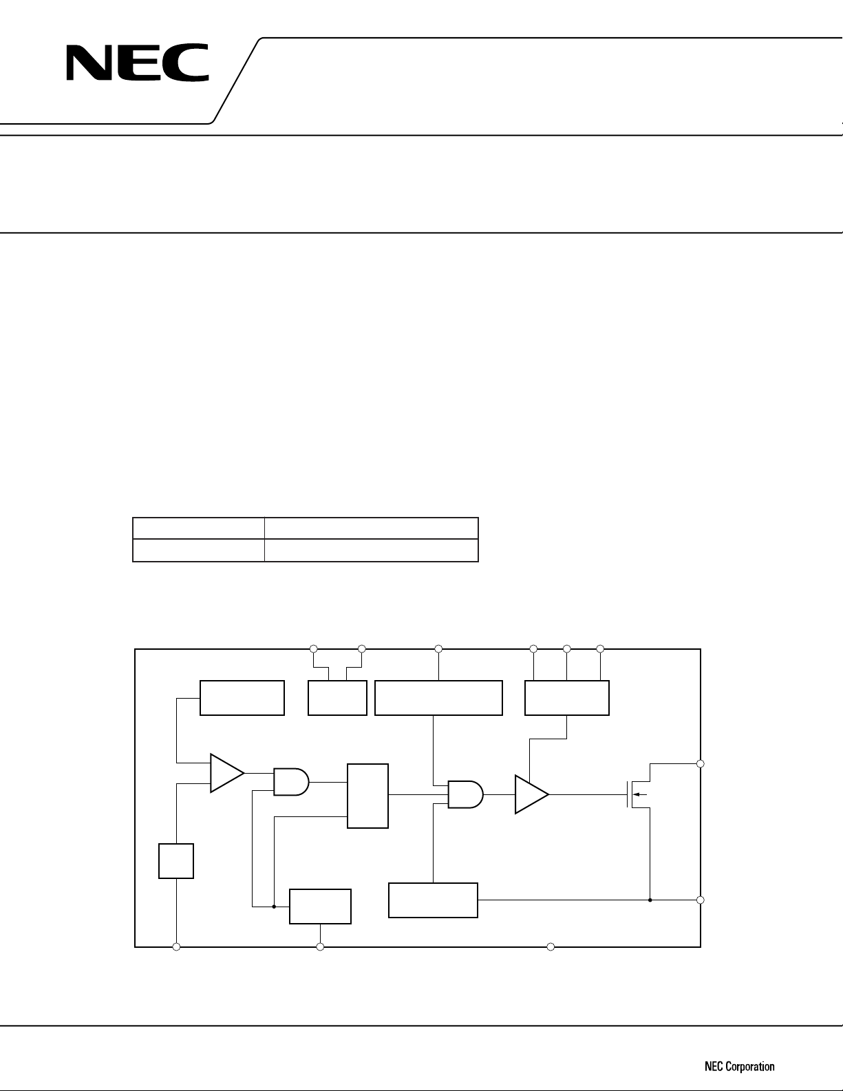
The µPD16901 is a DC/DC converter IC which produces a 12 V output from a 5 V input source. The integration
of a control circuit and power MOSFET in the output stage on a single-chip allows a power supply for flash memory
write and erasure to be configured with a reduced number of external components.
FEATURES
• With an on-chip output stage power MOSFET, fewer external components are needed.
• The ALLMOS structure achieves low power consumption.
• Internally set output voltage eliminates the need for adjustment.
• Output can be turned ON/OFF via an external signal.
• A timer latch type overcurrent protection circuit on chip
ORDERING INFORMATION
Part Number Package
µ
PD16901GS 14-pin plastic SOP (300 mil)
BLOCK DIAGRAM
Reference
voltage circuit
β
ON/OFF V
Startup
circuit
IN
Timer latch short-circuit
protection circuit
F/F
C
DLY
C1HC1LC
Charge pump
circuit
2
V
SW
SW
FB R
The information in this document is subject to change without notice.
Document No. S10643EJ2V0DS00 (2nd edition)
Date Published May 1997 N
Printed in Japan
Oscillation
circuit
T
Overcurrent
detection circuit
GND
C.S.
©
1997
Page 2
ABSOLUTE MAXIMUM RATINGS (TA = 25 ˚C unless specified otherwise)
Item Symbol Condition Rating Unit
Supply voltage VIN 7.0 V
Output voltage VSW 20 V
Total power dissipation PT Note 0.9 W
Operating ambient temperature TA –20 to 85 ˚C
Storage temperature range Tstg –55 to +150 ˚C
Note When 90 mm × 90 mm × 1.6 mm thick glass epoxy board is mounted
RECOMMENDED OPERATING RANGE
Item Symbol MIN. TYP. MAX. Unit
Supply voltage VDD 4.5 5.0 5.5 V
Charge pump capacitor C1, C2 0.033 0.1 0.47
Operating ambient temperature TA 070˚C
µ
F
µ
PD16901
ELECTRICAL SPECIFICATIONS (TA = 25 ˚C, VIN = 5 V unless specified otherwise)
Item Symbol Condition MIN. TYP. MAX. Unit
(Oscillation block)
Oscillation frequency fOSC RT = 68 kΩ 153 167 181 kHz
On duty DUTY 67 %
(Low voltage misoperation preventive circuit)
Operation start voltage VIN(start-up) 3.3 3.7 4.3 V
Operation stop voltage VIN(stop) 2.7 3.2 3.8 V
Hysteresis width VHYS 0.3 0.5 0.7 V
(Overcurrent detection block)
Overcurrent detection voltage VDET 270 300 330 mV
(On/off control block)
ON/OFF pin input voltage VIH 4.5 V ≤ VIN ≤ 5.5 V VIN*0.7 V
VIL 4.5 V ≤ VIN ≤ 5.5 V VIN*0.3 V
ON/OFF pin input current IIL ON/OFF pin voltage = 0 –20 –5 –1
(Charge pump circuit)
Output voltage VCHG 4.5 V ≤ VIN ≤ 5.5 V 8.0 11 V
0 ˚C ≤ TA ≤ 70 ˚C
(Short-circuit protection circuit)
Timer latch pin output current ISCP RT = 68 kΩ 2.0 3.3 4.5
Timer latch detection voltage VDETT 0.85 1.0 1.15 V
(Output block)
Output stage on resistance RDS(ON) IPK = 0.5 A 0.3 0.5 Ω
Output stage leakage current IDSOFF VDS = 20 V 1.0 µA
µ
A
µ
A
2
Page 3
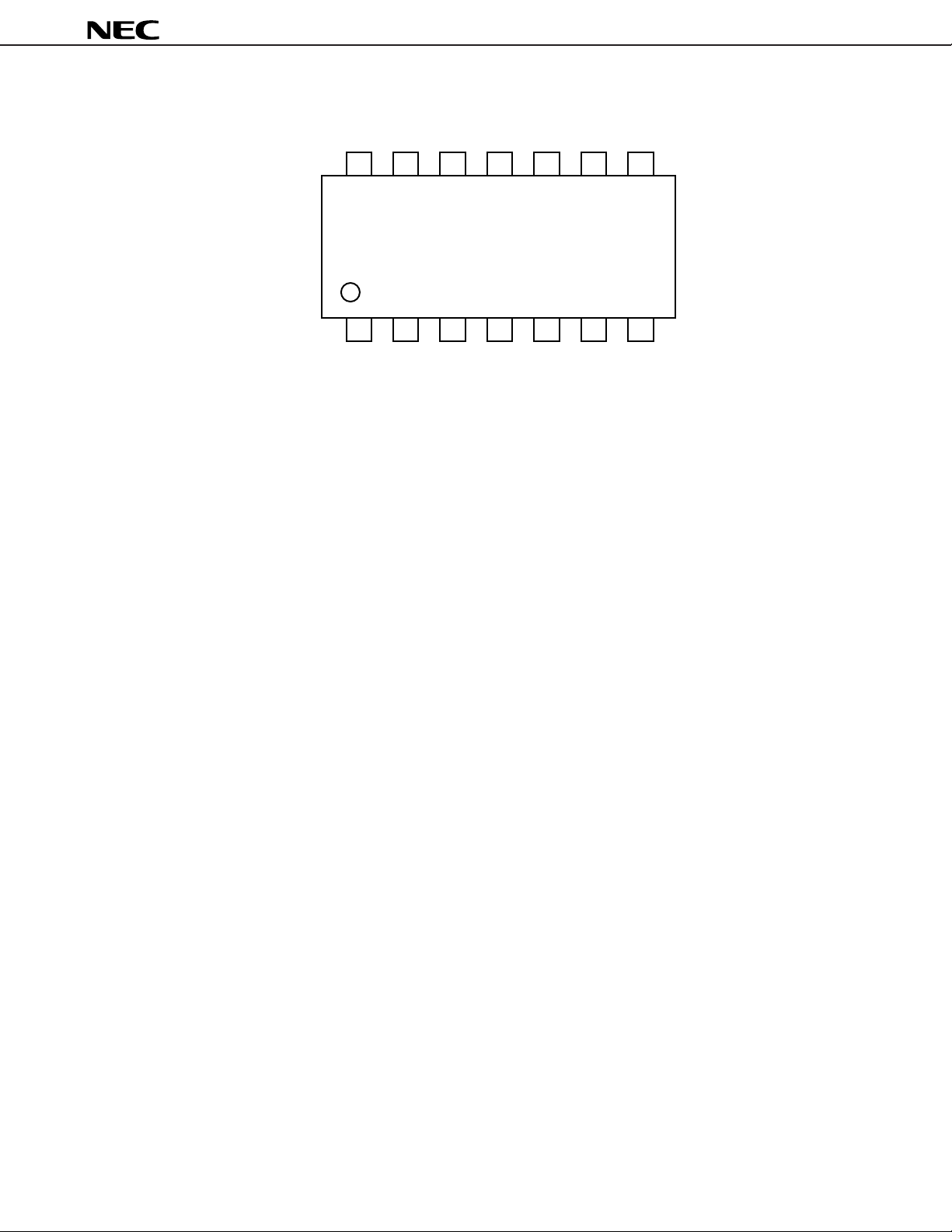
PIN CONFIGURATION (Top View)
C
14
µ
PD16901
V
2
NC11NC10NC9CS8FB
SW
13
12
1
C
2
3
C
1H
V
1L
CC
4
ON/OFF
5
R
6
C
T
DLY
7
GND
CONTROL
3
Page 4
PACKAGE DRAWINGS
14 PIN PLASTIC SOP (300 mil)
14 8
17
detail of lead end
P
µ
PD16901
A
G
F
E
C
M
D
NOTE
Each lead centerline is located within 0.12 mm (0.005 inch) of
its true position (T.P.) at maximum material condition.
M
B
H
I
J
K
L
ITEM MILLIMETERS INCHES
A
10.46 MAX.
B
1.42 MAX.
C
1.27 (T.P.)
D 0.40 0.016
E
F
G
H
I
J
K 0.20
L 0.6±0.2 0.024
M
N
P3° 3°
+0.10
–0.05
0.1±0.1
1.8 MAX.
1.55
7.7±0.3
5.6
1.1
+0.10
–0.05
0.12
0.10
+7°
–3°
P14GM-50-300B-4
0.412 MAX.
0.056 MAX.
0.050 (T.P.)
0.004±0.004
0.071 MAX.
0.061
0.303±0.012
0.220
0.043
0.008
0.005
0.004
+7°
–3°
N
+0.004
–0.003
+0.004
–0.002
+0.008
–0.009
4
Page 5

STANDARD CHARACTERISTIC CURVES
µ
PD16901
PT - TA characteristic
1.4
When mounted on
90 mm × 90 mm × 1.6 mm
glass epoxy board
(W)
T
1.2
1.0
0.9 W
0.8
0.6
0.4
Total Power dissipation P
0.2
0
–20 0 20 40 60 80 100
Ambient temperature TA (˚C)
CC (ON)
- VIN characteristic
I
3.5
TA = 85 ˚C
TA = 0 ˚C
(mA)
CC (ON)
3.0
2.5
2.0
139 ˚C/W
TA = 25 ˚C
85 ˚C
f
OSC
-VIN characteristic
180
175
(kHz)
OSC
170
165
160
Oscillation frequency f
155
3.5 4.0 4.5 5.0 6.0 6.5
5.5
Input voltage VIN (V)
f
OSC
- TA characteristic
180
175
(kHz)
170
OSC
165
T
A
= 25 ˚C
V
IN
= 5 V
1.5
1.0
0.5
Operating circuit current I
0
3.5 4.0 4.5 5.0 6.0 6.5
5.5
Input voltage VIN (V)
DET
- TA characteristic
V
340
(mV)
330
DET
320
310
300
290
280
Overcurrent detection voltage V
270
–20 0 20 40 60 80 100
Ambient temperature TA (˚C)
160
155
Oscillation frequency f
150
145
–20 0 20 40 60 80 100
Ambient temperature TA (˚C)
V
DETT
- TA characteristic
1.12
V
IN
= 5 V VIN = 5 V
(V)
DETT
1.1
1.08
1.06
1.04
1.02
1.0
Timer latch detection voltage V
0.98
–20 0 20 40 60 80 100
Ambient temperature TA (˚C)
5
Page 6

µ
( A)
SCP
µ
PD16901
SCP
- TA characteristic I
I
5
V
IN = 5 V
4
3
140
120
µ
( A)
100
CC (OFF)
80
CC (OFF)
- TA characteristic
IN = 5 V
V
2
1
Timer latch pin output current I
0
–20 0 40 60 100
20
Ambient temperature TA (˚C)
80
60
40
Standby current I
20
0
–20 0 20 40 60 80 100
Ambient temperature TA (˚C)
6
Page 7

STANDARD CONNECTION DIAGRAM
µ
PD16901
4.5 V to 5.5 V
ON/OFF
+
µ
C
33 F
IN
Reference
voltage circuit
β
Oscillation
circuit
FB R
68 kΩ
Startup
circuit
T
C
T
0.1 F
µ
V
IN
C
DLY
Timer latch short-circuit
protection circuit
F/F
Overcurrent
detection circuit
0.1 F
C
µ
C1HC1LC
Charge pump
circuit
GND
C
2
2
0.1 F
µ
L
33 H
µ
1
D
V
SW
SW
+
15 F
µ
C
OUT
C.S.
R
CS
0.3 Ω
Remark The circuit constants and circuit configuration in this connection diagram are shown for illustrative
purposes and not intended for volume production design.
ELECTRICAL SPECIFICATIONS
(as per standard connection diagram. T
Item Symbol Condition MIN. TYP. MAX. Unit
Output voltage VOUT 4.5 V ≤ VIN ≤ 5.5 V 11.52 12.00 12.48 V
Input stability REGIN 4.5 V ≤ VIN < 5.5 V 0.5 %/V
Load stability REGL 0 mA ≤ IO < 140 mA 0.004 %/mA
Conversion efficiency
Operating circuit current ICC IO = 0 3.0 mA
Standby circuit current ICC(OFF) ON/OFF pin voltage = 0 100
Startup voltage VIN(start-up) 3.7 4.3 V
η
A = 25 ˚C, VIN = 5 V, IOUT = 140 mA unless specified otherwise)
0 mA ≤ IO ≤ 140 mA
0 ˚C ≤TA ≤ 60 ˚C
83 %
Remark These specifications are reference values confirmed with the standard connection diagram (without
taking account of variations) and are not intended to guarantee the characteristics of the product as a
DC/DC converter.
µ
A
7
Page 8

STANDARD CHARACTERISTIC CURVES (as per standard connection diagram)
µ
PD16901
- IO characteristic
η
100
VIN = 5.5 V
80
η
VIN = 4.5 V
60
40
20
Conversion efficiency (%)
0
0 25 50 75 125 150100
Output current IO (mA)
V
O
- IO characteristic
13
12.5
(V)
O
12
Output voltage V
11.5
VIN = 5 V
IN
= 5V
V
O (MAX)
- VIN characteristic
I
350
300
(mA)
(MAX)
250
O
200
150
100
50
Maximum output current I
0
3.5 4.0 4.5 5.0 6.0 6.55.5
Input voltage VIN (V)
O
-TA characteristic
V
12.5
VIN = 5.5 V
(V)
O
12
11.5
Output voltage V
TA = 85 °C
TA = 0 °C
VIN = 4.5 V
TA = 25 °C
I
O
= 140 mA
VIN = 5 V
11
0 25 50 75 100
Output current IO (mA)
125 150
11
–20 0 20 40 60 80 100
Ambient temperature TA (°C)
8
Page 9

µ
PD16901
RECOMMENDED SOLDERING CONDITIONS
This product should be soldered and mounted under the conditions recommended below.
For soldering methods and conditions other than those recommended, please contact your NEC sales representative.
For details of recommended soldering conditions, refer to the information document "Semiconductor Device
Mounting Technology Manual."
Soldering Method Soldering Conditions
Infrared reflow Package peak temperature: 235 ˚C; Duration: 30 sec. max. (210 ˚C or above): IR35-00-3
Number of times: Max. 3; Time limit: None
Flux: Rosin type flux with reduced chlorine content (chlorine 0.2 Wt% or less)
is recommended.
VPS Package peak temperature: 215 ˚C; Duration: 40 sec. max. (200 ˚C or above): VP15-00-1
Number of times: 1; Time limit: None
Flux: Rosin type flux with reduced chlorine content (chlorine 0.2 Wt% or less)
is recommended.
Wave soldering Package peak temperature: 260 ˚C or less, Duration: 10 sec. max., WS60-00-1
Preparatory heating temperature: 120 ˚C or less; Number of times: 1
Flux: Rosin type flux with reduced chlorine content (chlorine 0.2 Wt% or less)
is recommended.
Note
Note
Recommended
Condition Symbol
Note For the storage period after unpacking from the dry-pack, storage conditions are max. 25 ˚C, 65% RH.
Caution Use of more than one soldering method should be avoided.
REFERENCE DOCUMENTS
NEC Semiconductor Device Reliability/Quality Control System 10983E
Semiconductor Device Quality Guarantee Guide MEI-1202
Semiconductor Device Mounting Technology Manual C10535E
9
Page 10

[MEMO]
µ
PD16901
10
Page 11

[MEMO]
µ
PD16901
11
Page 12

µ
PD16901
No part of this document may be copied or reproduced in any form or by any means without the prior written
consent of NEC Corporation. NEC Corporation assumes no responsibility for any errors which may appear in
this document.
NEC Corporation does not assume any liability for infringement of patents, copyrights or other intellectual property
rights of third parties by or arising from use of a device described herein or any other liability arising from use
of such device. No license, either express, implied or otherwise, is granted under any patents, copyrights or other
intellectual property rights of NEC Corporation or others.
While NEC Corporation has been making continuous effort to enhance the reliability of its semiconductor devices,
the possibility of defects cannot be eliminated entirely. To minimize risks of damage or injury to persons or
property arising from a defect in an NEC semiconductor device, customers must incorporate sufficient safety
measures in its design, such as redundancy, fire-containment, and anti-failure features.
NEC devices are classified into the following three quality grades:
"Standard", "Special", and "Specific". The Specific quality grade applies only to devices developed based on a
customer designated "quality assurance program" for a specific application. The recommended applications of
a device depend on its quality grade, as indicated below. Customers must check the quality grade of each device
before using it in a particular application.
Standard: Computers, office equipment, communications equipment, test and measurement equipment,
audio and visual equipment, home electronic appliances, machine tools, personal electronic
equipment and industrial robots
Special: Transportation equipment (automobiles, trains, ships, etc.), traffic control systems, anti-disaster
systems, anti-crime systems, safety equipment and medical equipment (not specifically designed
for life support)
Specific: Aircrafts, aerospace equipment, submersible repeaters, nuclear reactor control systems, life
support systems or medical equipment for life support, etc.
The quality grade of NEC devices is "Standard" unless otherwise specified in NEC's Data Sheets or Data Books.
If customers intend to use NEC devices for applications other than those specified for Standard quality grade,
they should contact an NEC sales representative in advance.
Anti-radioactive design is not implemented in this product.
M4 96.5
 Loading...