

Page 1

DATA SHEET
MOS INTEGRATED CIRCUIT
µµµµ
PD16879
MONOLITHIC QUAD H BRIDGE DRIVER CIRCUIT
The
PD16879 is a monolithic quad H bridge driver IC that employs a CMOS control circuit and a MOSFET output
µ
circuit. Because it uses MOSFETs in its output stage, this driver IC consumes less power than conventional driver
ICs that use bipolar transistors.
Because the µPD16879 controls a motor by inputting serial data, its package has been shrunk and the number of
pins reduced. As a result, the performance of the application set can be improved and the size of the set has been
reduced.
This IC employs a current-controlled 64-step micro step driving method that drives stepper motor with low
vibration.
The µPD16879 is a housed in a 38-pin shrink SOP to contribute to the miniaturization of application set.
This IC can simultaneously drive two stepper motors and is ideal for the mechanisms of camcorders.
FEATURES
Four H bridge circuits employing power MOS FETs
•
Current-controlled 64-step micro step driving
•
Motor control by serial data (8 bits × 13 bytes)
•
PWM-frequency, output current and number of output pulse can be setting by serial data.
3-V power supply.
•
Minimum operating voltage: 2.7 V
Low consumption current.
•
DD
V
pin current (operating mode) : 3 mA (MAX.)
Power save circuit bult in.
•
VDD pin current (power save mode) : 100 µA (MAX.) f
VDD pin current (power save mode) : 300 µA (MAX.) f
38-pin shrink SOP (7.62 mm (300))
•
CLK
: OFF state
CLK
: 4.5 MHz input
ORDERING INFORMATION
Part Number Package
PD16879GS-BGG 38-pin plastic shrink SOP (7.62 mm (300))
µ
The information in this document is subject to change without notice. Before using this document, please
confirm that this is the latest version.
Not all devices/types available in every country. Please check with local NEC representative for
availability and additional information.
Document No. S14188EJ1V0DS00 (1st edition)
Date Published July 2000 N CP(K)
Printed in Japan
©
2000
Page 2
ABSOLUTE MAXIMUM RATINGS (TA = +25°C)
µµµµ
PD16879
When mounted on a glass epoxy board (100 mm
100 mm
××××
Parameter Symbol Conditions Rating Unit
DD
Input voltage V
Reference voltage V
I
M(pulse)
I
Power consumption P
Peak junction temperature T
CH(MAX)
Storage temperature T
V
V
M(DC)
Control part –0.5 to +6.0 VSupply voltage
M
Output part –0.5 to +11.2 V
IN
REF
External input 0.5 V
DC
PW < 10 ms, Duty < 5 %
T
stg
RECOMMENDED OPERATING RANGE (TA = +25°C)
When mounted on a glass epoxy board (100 mm
Parameter Symbol Conditions MIN. TYP. MAX. Unit
DD
V
V
Input voltage V
Reference voltage V
EXP pin input voltage V
EXP pin input current I
Clock frequency (OSCIN)f
EXPIN
EXPIN
M(DC)
I
M(pulse)
I
CLK
Clock frequency amplit ude V
Serial clock frequency f
SCLK
Video sync signal widt h PW
LATCH signal wait time t
SCLK wait time t
SDATA setup time t
SDATA hold time t
Reset signal pulse width t
(VD-LATCH)
(SCLK-LATCH)
setup
hold
RST
Operating temperautre T
Peak junction temperature T
CH(MAX)
Control part 2.7 5.5 VSupply voltage
M
Output part 4.0 11 V
IN
REF
External input 225 250 275 mV
DC
PW < 10 ms, Duty < 5%
OSC
C
fCLK
(VD)fCLK
Refer to Fig. 1
A
100 mm
××××
= 68 pF, V
REF
= 250 mV 3.9 4.5 6.0 MHz
= 4.5 MHz 250 ns
1 mm, 15% copper foil)
××××
–0.5 to VDD + 0.5 V
0.15 A/chH bridge drive current
±
0.3 A/ch
±
1.0 W
150
–55 ∼ +150
1 mm, 15% copper foil)
××××
−
−
0.7 × V
400 ns
400 ns
100
−
C
°
C
°
V
100
DD
DD
V
V
A
µ
0V
0.1 +0.1 A/chH bridge drive current
0.2 +0.2 A/ch
DD
DD
V
V
5.0 MHz
80 ns
80 ns
s
µ
10 85
125
C
°
C
°
2
Data Sheet S14188EJ1V0DS00
Page 3
ELECTRICAL CHARACTERISTICS
(Unless otherwise specified, TA = 25
REF
V
= 250 mV, EVR = 100 mV (10000))
Parameter Symbol Conditions MIN. TYP. MAX. Unit
°°°°
C, VDD = 3 V, VM = 5.4 V, f
CLK
= 4.5 MHz, C
OSC
= 68 pF, C
µµµµ
PD16879
FIL
= 1000 pF,
Off state VM pin current I
MO(RESET)
Operating state VDD pin current I
VDD pin current I
DD(RESET)
DD(PS)1tCLK
I
DD(PS)2fCLK
I
High level input voltage V
Low level input voltage V
Input hysteresis vosltage V
V
(EXTOUT
α, β
)
V
V
V
OEXP(H)
V
(EXP 0,1 open drain)
OEXP(L)IOEXP
V
High level input current I
Low level input current I
Reset pin high level input c urrent I
Reset pin low level input c urrent I
IH(RST)
IL(RST)
H bridge ON resistance R
Chopping frequency
Note 1
Internal reference voltage V
VD delay time
Sin wave peak output current
(reference value)
FIL pin voltage
FIL pin step voltage
H bridge turn on time
H bridge turn off time
Note 2
Note 4
Note 3
Note 4
Note 5
Note 5
V
EVRSTEP
V
t
DD
IH
IL
H
OMα(H)
OMβ(H)
OMα(L)
OMβ(L)
IH
IL
ON
OSC
f
REF
VD
t
∆
M
I
EVR
ONH
t
OFFH
No load, Reset period 1.0
A
µ
Output open 3.0 mA
Reset period 100
= off 100
= 4.5 MHZ 300
LATCH, SCLK, SDATA, VD, V
RESET, OSCIN, V
REFsel
D
0.7 × V
DD
0.3 × V
A
µ
APower save state VDD pin current
µ
A
µ
V
DD
V
0.3 V
DD
4th byte
Pull up (VDD)0.9
= 100 µA0.1
DD
VIN = V
VIN = 0
RST
RST
= V
= 0
DD
V
V
0.9 × V
0.3 0.1 × V
−
DD
V
×
1.0
−
1.0
−
×
1.0
1.0
V
IM = 100 mA, upper + lower 6.0
VMonitor output voltage 1
DD
V
VMonitor output voltage 2
DD
V
A
µ
A
µ
A
µ
A
µ
Ω
Refer to table 1 (TYP.) kHz
225 250 275 mV
250 ns
L = 15 mH/R = 70 Ω ( 1 kHz)
S
R
= 6.8 Ω, f
OSC
= 72.58 kHz
53 mA
EVR = 220 mV (11100)
EVR = 200 mV (11010)
REF
V
= 250 mV external input
370 400 430 mV
Minimum step 20 mV
IM = 100 mA
2.0
2.0
s
µ
s
µ
Notes 1.
When data are less than 7 (000111), PWM chopping doesn’t do it, and output pulse doesn’t occur.
When data are beyong 49, PWM chopping frequency becomes a 225 kHz fixation.
IN
By OSC
2.
FB pin is monitored.
3.
FIL pin is monitored. A voltage about twice that of the EVR value is output to the FIL pin.
4.
10% to 90% of the pulse peak value without filter capacitor (C
5.
and VD sync circuit
Data Sheet S14188EJ1V0DS00
FIL
)
3
Page 4
µµµµ
PD16879
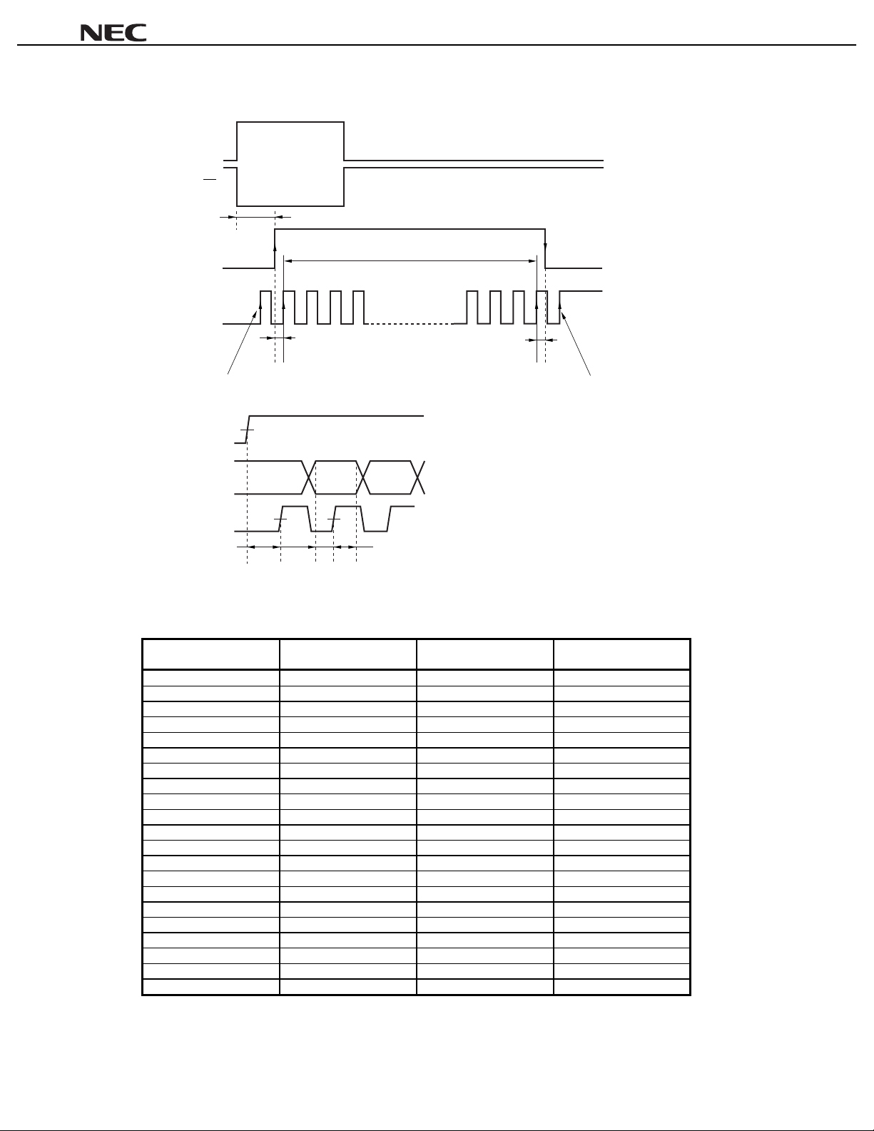
Fig 1. Delay Time of Serial Data
D
V
V
D
(VD-LATCH)
t
LATCH
104 clocks (8 bits × 13 bytes)
SCLK
t
t
(SCLK-LATCH)
Ignored because LATCH is at low level
LATCH
SDATA
SCLK
50%
50%
t
(SCLK-LATCH)
D1 D2
50%
t
setup
D3
t
hold
Table 1. Chopping Frequency (3rd byte D5 to D0 bit data, f
Input data
D5 to D0 bit
Chopping frequency
(kHz)
(SCLK-LATCH)
Ignored because LATCH is at low level
= 4.5 MHz) Typical Value
CLK
Input data
D5 to D0 bit
001000 35.71 011101 132.35
001001 40.18 011110 132.35
001010 45.00 011111 140.63
001011 50.00 100000 140.63
001100 53.57 100001 150.00
001101 59.21 100010 150.00
001110 62.50 100011 160.71
001111 68.18 100100 160.71
010000 72.58 100101 160.71
010001 77.59 100110 173.08
010010 80.36 100111 173.08
010011 86.54 101000 173.08
010100 90.00 101001 187.50
010101 93.75 101010 187.50
010110 97.83 101011 187.50
010111 102.27 101100 204.55
011000 107.14 101101 204.55
011001 112.50 101110 204.55
011010 118.42 101111 204.55
011011 118.42 110000 225.00
011100 125.00
Chopping frequency
(kHz)
When data are less than 7 (000111), PWM chopping doesn’t do it, and output pulse doesn’t occur.
Note
When data are beyond 49, PWM chopping frequency becomes a 225 kHz fixation.
4
Data Sheet S14188EJ1V0DS00
Page 5

Table 2. Relation Between Rotation Angle, Phase Current, and Vector Quantity
(64-DIVISION MICRO STEP)
(Value of
PD16879 for reference)
µ
A phase current B phase current Vector quantitySTEP Rotation angle (θ)
MIN. TYP. MAX. MIN. TYP. MAX. TYP.
00
θ
1 5.6 2.5 9.8 17.0
θ
2 11.3 12.4 19.5 26.5 93.2 98.1 103 100
θ
3 16.9 22.1 29.1 36.1 90.7 95.7 100.7 100.02
θ
4 22.5 31.3 38.3 45.3 87.4 92.4 97.4 100.02
θ
5 28.1 40.1 47.1 54.1 83.2 88.2 93.2 99.99
θ
6 33.8 48.6 55.6 62.6 78.1 83.1 88.1 99.98
θ
7 39.4 58.4 63.4 68.4 72.3 77.3 82.3 99.97
θ
8 45 65.7 70.7 75.7 65.7 70.7 75.7 99.98
θ
9 50.6 72.3 77.3 82.3 58.4 63.4 68.4 99.97
θ
10 56.3 78.1 83.1 88.1 48.6 55.6 62.6 99.98
θ
11 61.9 83.2 88.2 93.2 40.1 47.1 54.1 99.99
θ
12 67.5 87.4 92.4 97.4 31.3 38.3 45.3 100.02
θ
13 73.1 90.7 95.7 100.7 22.1 29.1 36.1 100.02
θ
14 78.8 93.2 98.1 103 12.4 19.5 26.5 100
θ
15 84.4
θ
16 90
θ
−
−
−
0
100
100
−−
−
−
−−
2.5 9.8 17.0 100.48
100
100
0
−
−
−
µµµµ
PD16879
100
100.48
100
Remark
These data do not indicate guaranteed values.
Data Sheet S14188EJ1V0DS00
5
Page 6
PIN CONFIGURATION
µµµµ
PD16879
10
11
12
13
14
15
16
17
18
19
1
LGND
2
3
4
5
6
7
8
9
C
FIL
FIL
FIL
FIL
V
V
V
D
FB
D
V
C
FB
C
OSC
A
B
C
D
REF
DD
M3
2
D
1
M4
2
C
1
EXP0
EXP1
REFsel
V
RESET
OSC
OSC
SCLK
SDATA
LATCH
FB
V
FB
V
EXT
EXT
PGND
OUT
V
V
38
37
IN
36
35
34
33
D
32
D
31
B
2
30
B
29
B
1
28
M2
27
A
2
26
A
25
A
1
24
M1
23
β
22
21
α
20
6
Data Sheet S14188EJ1V0DS00
Page 7

PIN FUNCTION
Package: 38-pin plastic shrink SOP
Pin Pi n name Pin function
1 LGND Control circuit GND pi n
2C
3FIL
4FIL
5FIL
6FIL
7V
8VDDControl circuit supply voltage input pin
9VM3Output circuit supply voltage input pin
10 D
11 FB
12 D
13 V
14 C
15 FB
16 C
17 EXP0 External extension pin (open drain)
18 EXP1 External extension pin (open drain)
19 V
20 P GND Out put circuit GND pin
21 EXT
22 EXT
23 V
24 A
25 FB
26 A
27 V
28 B
29 FB
30 B
31 V
32 V
33 LATCH LATCH signal input pin
34 SDATA Serial data input pi n
35 SCLK Serial clock input pin (4.5 MHz typ)
36 OSC
37 OSC
38 RESET Reset signal input pin
OSC
A
B
C
D
REF
2
D
1
M4
2
C
1
REFsel
αα
ββ
M1
1
A
2
M2
1
B
2
D
D
IN
OUT
Chopping capacitor connection pi n
1 ch filter capacitor connection pin
α
2 ch filter capacitor connection pin
α
1 ch filter capacitor connection pin
β
2 ch filter capacitor connection pin
β
Reference voltage input pin (250 mV typ)
2 ch output pin
β
2 ch sense resistor connection pin
β
2 ch output pin
β
Output circuit supply voltage input pin
1 ch output pin
β
1 ch sense resistor connection pin
β
1 ch ouptut pin
β
Reference voltage select pi n
ch logic circuit m oni tor pin
ch logic circuit m oni tor pin
Output circuit supply voltage input pin
1 ch output pin
α
1 ch sense resistor connection pin
α
1 ch output pin
α
Output circuit supply voltage input pin
2 ch output pin
α
2 ch sense resistor connection pin
α
2 ch output pin
α
Video sync signal input pi n
Video sync signal input pi n
Original oscillation input pin (4.5 MHz typ)
Original oscillation output pin
Note 2
Note 2
Note 1
Note 1
µµµµ
PD16879
Remark
Notes 1.
M
Plural terminal (V
) is not only 1 terminal and connect all terminals.
A standard voltage to use is chosen.
REFsel
V
: High level using external input V
REFsel
V
: Low level using internal reference voltage (V
Input the video sync singnal to VD pin or VD pin. A free terminal is to do the following treatment.
2.
REF
REF
pin fixed GND level)
When input VD: VD pin connect to VDD pin.
When input VD: VD pin connect to GND pin.
Data Sheet S14188EJ1V0DS00
7
Page 8
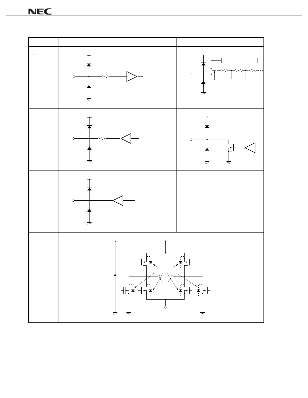
I/O PIN EQUIVALENT CIRCUIT
Pin name Equival ent circuit Pin name Equivalent circuit
µµµµ
PD16879
D
V
D
V
LATCH
SDATA
SCLK
IN
OSC
RESET
REFsel
V
OUT
OSC
α
EXT
β
EXT
A
FIL
B
FIL
C
FIL
D
FIL
PAD
PAD
PAD
REF
V
DD
V
V
DD
Internal 250 mV
PAD
V
REFsel
EXP0
V
V
DD
EXP1
DD
PAD
V
DD
A1, A
B1, B
C1, C
D1, D
Buffer
2
2
2
2
VM
Parasitic diodes
PAD
FB
8
Data Sheet S14188EJ1V0DS00
Page 9
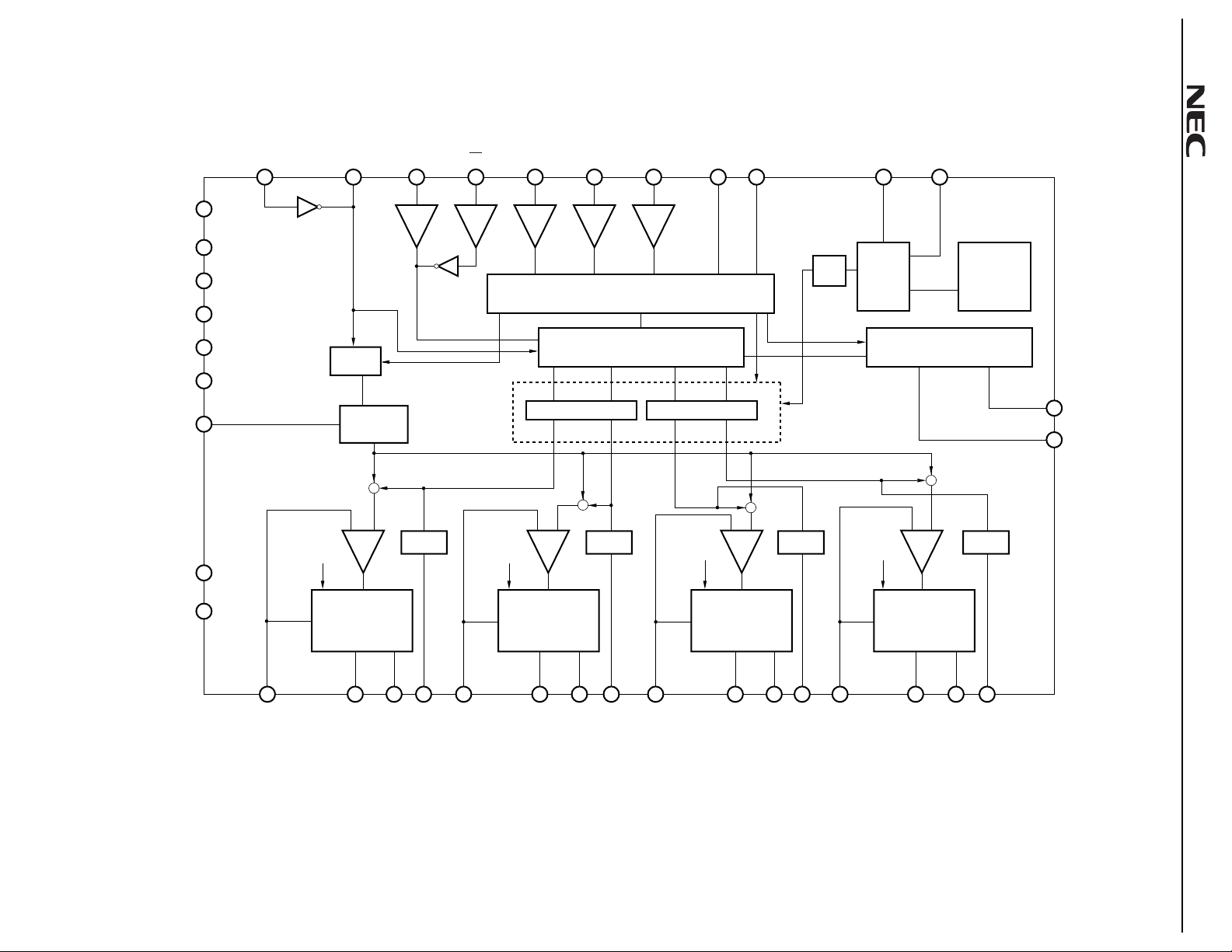
BLOCK DIAGRAM
Remark
OSC
OSC
IN
OUT
V
D
V
D
SCLK
SDATA LATCH
EXP0
EXP1
V
REFsel
V
REF
Plural terminal (V
M
) is not only 1 terminal and connect all terminals.
RESET
V
V
V
V
36
37
32 31 35 34 33
38
8
DD
M1
23
SERIAL-PARARELLE DECODER
M2
27
9
M3
PULSE GENERATER
17
18
× 2
19
7
Vref
select
EXTOUT SELECTOR
250 mV
B.G.R
1/N
V
Data Sheet S14188EJ1V0DS00
C
OSC
LGND
PGND
13
M4
21
22
FILTER
α
CURRENT SET
2
V
OSC
+
+
–
M
FILTER
CURRENT SET
–
V
M
+
+
β
+
+
+
–
V
M
FILTER
V
+
–
M
FILTER
EXT
EXT
EXT
α
β
1
20
H BRIDGE
α
1ch
H BRIDGE
2ch
α
H BRIDGE
β
1ch
H BRIDGE
2ch
β
25 24 26
A
FB
A
1
3
29
FIL
A
A
2
FB
B
28
30 4
B
1
FIL
B
2
15 16 14 5
B
FB
C
C2FIL
C
1
11
C
FB
D
12
D
1
6
10
FIL
D
D
2
µµ
µ
µ
PD16879
9
Page 10
10
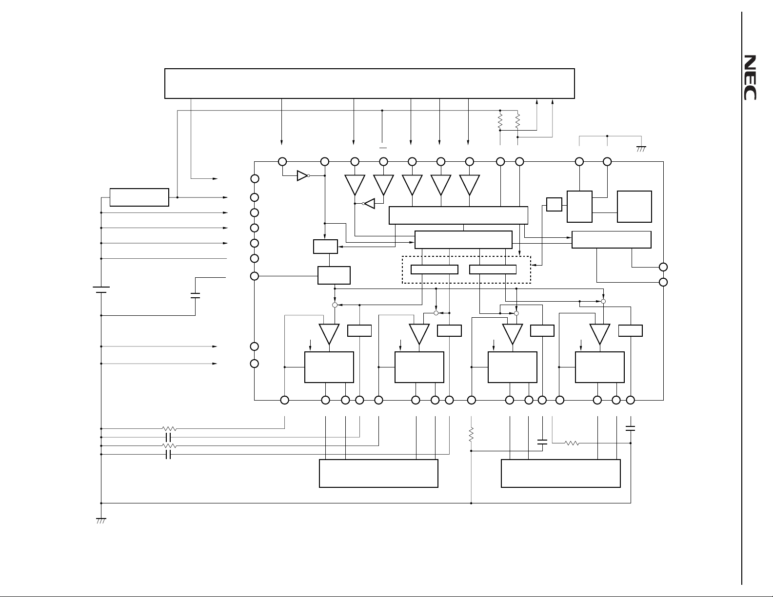
EXAMPLE OF STANDARD CONNECTION
CPU
100 kΩ × 2
4.5 MHz TYP.
V
D
V
D
IN
OSC
OSC
36
V
V
V
V
V
OSC
38
DD
8
M1
23
27
M2
M3
9
13
M4
2
RESET
REGULATOR
Data Sheet S14188EJ1V0DS00
2.7 V to 5.5 V
C
OUT
37 32 31 35 34 33
1/N
OSC
SCLK
SDATA LATCH
SERIAL-PARALLELE DECODER
PULSE GENERATOR
CURRENT SET CURRENT SET
α
EXP0
EXP1
17
β
18
BATTERY
4.0 V to 11 V
68 pF
LGND
PGND
1
20
25
+
–
V
M
H BRIDGE
1ch
α
24
+
+
+
FILTER
–
V
M
FILTER
V
H BRIDGE
1ch
α
26
30
3
29
28
4
15 16
+
+
–
M
H BRIDGE
1ch
β
FILTER
14
Using internal reference
V
REFselVREF
19
7
× 2
Vref
select
250 mV
B.G.R
EXTOUT SELECTOR
+
+
–
V
M
FILTER
H BRIDGE
1ch
β
511 12106
21
22
EXT
EXT
α
β
6.8 Ω × 2
1000 pF × 2
FB
C
A
1
A
2
FIL
A
FB
A
B
B2FIL
B
1
B
FB
C
6.8 Ω
2
FILCFB
C
1
D
6.8 Ω
D1D2FIL
D
1000 pF
1000 pF
µµ
µ
MOTOR 1
MOTOR 2
µ
PD16879
Page 11

Initialization
TIMING CHART (1)
RESET
V
D
V
D
S1 S2
S3
S4
pulse 0
S5
S9
PS
S6
PS
S7
release PS
S8
Enable
S10
release PS
S11 S12
data error
S13
normal data
S14
LATCH
DATA
SCLK
OSC
OUT
Start point wait
(FF1)
Data Sheet S14188EJ1V0DS00
Start point wait+
Start point magnetize wait
(FF2)
S1
S2
S2
S3
S3
S4
S4
S4
H level fixation
It reverts from the VD
start after a PS release.
L level fixation
S7
S8
S8
S9
S9
S10
S10
S11
S11
S12
S12
S13
S13
S14
11
ENABLE OUT
Note 1
CHOPPING
EXP 0, 1
PULSE OUT
PULSE GATE
(FF3)
PULSE CHECK
Note 2
(FF7)
CHECK SUM
Note 3
SCLK
SDATA
1st byte → 13th byte
D0
D1 D2
(LSB)
Data is held at rising edge SCLK
L level fixation
Stop from
LATCH ↓
EXP can be change in PS period too.
S2
S3
S4
Pulse is nothing
because pulse
data is "0"
Start from
LATCH ↓
S5 to S7
Pulse is nothing
because PS data
Notes 1.
Pulse count is done
S8
in enable period too
S11S10S9
Pulse is nothing
because
error data.
Output L level
because
error data
S13
ENABLE is set at the falling edge of FF1 when the level changes from
low to high, and at the falling edge of FF2 when the level changes from
D3
D4 D5 D6 D7
high to low.
2.
FF7 is an output signal that is used to check for the presence or
absence of a pulse in the serial data, is updated at the falling edge of
µµ
µ
µ
PD16879
LATCH and reset once at the rising edge of LATCH. If CHECK SUM
is other than "00h", FF7 goes low, inhibiting pulse output, even if a
pulse is generated.
3.
CHECK SUM output is updated at the falling edge of LATCH.
Page 12

TIMING CHART (2)
CLK
(PULSE OUT)
MOB
(CW mode)
µµµµ
PD16879
H bridge ,
H bridge ,
α
1ch output
α
2ch output
CLK
PULSE OUT
Position No.
Current direction: A2 to A1
β
Current direction: A1 to A2
Current direction: B2 to B1 Current direction: B2 to B1
β
Current direction: B1 to B2
(Expanded view)
CCW mode
65
CCW
CW mode
3
4
23
CCW
CW
4
CW mode : Position No is inc rem ented.
Note
CCW mode: Position No is decremented
H bridge
1ch output
CW mode
1
2
3
CW
4
5
.
Remarks 1.
12
CW
CW
H bridge
2ch output
CW
CCW
CW
CCW
The current value of the actual wave is approximated to the value shown on the page 5.
The C1, C2, D1, and D2 pins of
2.
The CW mode is set if the D6 bit of the fifth and ninth bytes of the data is “0”.
3.
The CCW mode is set if the D6 bit of the fifth and ninth bytes of the data is “1”.
4.
channel correspond to the A1, A2, B1, and B2 pins of α channel.
β
Data Sheet S14188EJ1V0DS00
Page 13

STANDARD CHARACTERISTICS CURVES
PT vs. TA characteristics
1.2
1.0
(W)
T
0.8
125°C/W
0.6
0.4
Total power dissipation P
0.2
7.0
6.0
5.0
(mA)
DD
4.0
3.0
pin current I
DD
2.0
V
1.0
I
DD
vs. VDD characteristics
µµµµ
PD16879
T
A
= 25°C
operating
0
–20 0 20 40
Ambient temperature T
DD(RESET)
I
350
µ
300
( A)
250
DD(RESET)
200
150
100
pin current (RESET) I
50
DD
V
0
123
Control circuit supply voltage V
IH
, VIL vs. VDD characteristics
V
4.0
80
60
A
(°C)
vs. VDD characteristics
A
T
RESET
5
4
DD
T
A
100 120
= 25°C
6
(V)
= 25°C
0
123
Control circuit supply voltage V
µ
600
( A)
500
DD(PS2)
, I
400
DD(PS1)
300
200
pin current (PS) I
100
DD
V
0
123
Control circuit supply voltage V
254
253
I
DD(PS)
vs. VDD characteristics
I
V
REF
vs. TA characteristics
4
I
DD(PS)2
DD(PS)1
4
5
DD
(V)
T
A
= 25°C
PS mode
5
DD
(V)
DD
= 3.0 V
V
V
FIL
/2
6
6
(V)
IL
3.0
, V
IH
2.0
Input voltage V
1.0
0
123
Control circuit supply voltage V
252
(mA)
REF
251
IL
V
V
IH
250
249
248
247
Reference voltage V
246
6
245
5
4
DD
(V)
Data Sheet S14188EJ1V0DS00
02040
Ambient temperature T
60
80
A
(°C)
100
120–20
13
Page 14

µµµµ
PD16879
70
60
50
40
30
20
10
Sine wave peak output current IM (mA)
0
60
50
40
IM vs. EVR characteristics
TA = 25°C, 70 Ω, 15 mV, VM = 5.4 V
RS = 6.8 Ω, fOSC = 72.58 kHz
50 100 150
200
EVR setting voltage EVR (mV)
M vs. RS characteristics
I
TA = 25°C, 70 Ω, 15 mH, VM = 5.4 V
fOSC = 72.58 kHz, EVR = 100 mV (10000)
250
50
40
30
20
10
Sine wave peak output current IM (mA)
0
8.0
6.0
M vs. VM characteristics
I
TA = 25°C, 70 Ω, 15 mH, RS = 6.8 Ω
fOSC = 72.58 kHz, EVR = 100 mV (10000)
246
10
8
Output circuit supply voltage VM (V)
ON vs. VM characteristics
R
T
A = 25°C
12
30
20
10
Sine wave peak output current IM (mA)
0
8.0
6.0
4.0
2.0
H bridge ON resistance RON (Ω)
4
2
6810
Current sense resistor RS (Ω)
ON vs. TA characteristics
R
12
V
M = 4.0 V
M = 5.4 V
V
V
M = 8.0 V
V
M = 11 V
14
4.0
2.0
H bridge ON resistance RON (Ω)
0
4
2
6810
12
Output circuit supply voltage VM (V)
14
0
–20
40 60 80
20
0
Ambient temperature TA (°C)
120
100
Data Sheet S14188EJ1V0DS00
Page 15

µµµµ
PD16879
I/F CIRCUIT DATA CONFIGURATION (f
CLK
= 4.5 MHz EXTERNAL CLOCK INPUT)
Input data consists of serial data (8 bits × 13 bytes).
Input serial data with the LSB first, from the first byte to 13th byte.
[1st byte] [2nd byte]
Bit Data Function Setting Bit Data Function Setting
D7 D7
D6 D6
D5 D5
D4 D4
D3 D3
8 bit data
Note
input
First point
wait
First point wait
227.6
s to
µ
58.03 ms
Setting
(1 to 255)
t = 227.6 µs
∆
8 bit data
Note
input
First point
magnetize
wait
D2 D2
D1 D1
D0
Input other than “0”
Note
D0
Input other than “0”
Note
[3rd byte] [4th byte]
Bit Data Function Setting Bit Data Function Setting
Note 1
D7 1 or 0 EXP1
D6 1 or 0 EXP0
D5 D6
D4 D5
6 bit data
input
Chopping
frequency
D3 D4
D2 D3
D1 D2
D0
Z/L
Note 1
Z/L
Chopping
frequency
35.71 kHz to
225 kHz
Setting
Note 2
(8 to 48)
D7 1 or 0 Power save
Bit Data EXT α Output EXT β Output
Note 2
Enable
Note 3
Rotation
Pulse out Pulse out
FF7 FF7
FF3 FF3
Checksum
Note 4
D1
Note 5
Note 5
Note 5
Note 5
Note 5
Note 5
First point
magnetize
wait
227.6
s to
µ
58.03 ms
Setting
(1 to 255)
t = 227.6 µs
∆
OFF/ON
Note 2
Enable
Rotation
FF2
Note 1
Note 3
Notes 1.
Z: High impedance/L: low level
0 to 7 input: PWM and pulse out nothing
2.
49 to 63 input: 225 kHz fixed
Refer to 4 page
Data Sheet S14188EJ1V0DS00
D0
Notes 1.
Note 5
Chopping FF1
Data “1”: Normal/Data “0”: Power save
High: Conducts/Low: Stops
2.
High: Reverse (CCW)/Low: Forward (CW)
3.
High: Normal data/Low: Error data
4.
Select one of D0 to D6 and input ”1”.
5.
If two or more of D0 to D6 are selected,
they are positively ORed for output.
15
Page 16

[5th byte] [6th byte]
Bit Data Function Setting Bit Data Function Setting
µµµµ
PD16879
D7 1 or 0 Enable
D6 1 or 0 Rotation
D5 0 Not use Not use D5
D4 D4
D3 D3
D2 D2
D1 D1
D0
Note
5 bit data
input
Fixed to 50 mV if 0 to 10 input.
αα
channel
α
Current set
αα
ch ON/OFF D7
ch CCW/CW D6
channel
α
Current set
EVR: 50 to
250 mV
Setting
(11 to 31)
Note
Refer to 4 page.
D0
Note
8 bit data
input
channel
α
Pulse
Number
Output pulse is nothing if data input 256, 512,
and 768.
[7th byte] [8th byte]
Bit Data Function Setting Bit Data Function Setting
D7 D7
D6 D6
D5 D5
D4 D4
D3 D3
D2 D2
D1 D1
D0
16 bti data
low-order
8 bit data
input
channel
α
Pulse Cycle
channel
α
Pulse cycle
222 ns to
14.563 ms
Setting (1 to
65535)
t = 222 ns
∆
D0
16 bit data
High-order
8 bit data
input
channel
α
Pulse Cycle
channel
α
Number of
pulse in 1 V
0 to 1020
pulses
Setting (0 to
255)
n = 4
∆
Note
pulses
channel
α
Pulse cycle
222 ns to
14.563 ms
Setting (1 to
65535)
t = 222 ns
∆
D
D0 bit of 7th byte is LSB, and D7 bit of 8th byte is MSB.
Note
[9th byte] [10th byte]
Bit Data Function Setting Bit Data Function Setting
D7 1 or 0 Enable
D6 1 or 0 Rotation
D5 0 Not use Not use D5
D4 D4
D3 D3
D2 D2
D1 D1
D0
Note
5 bit data
input
Fixed to 50 mV if 0 to 10 input.
ββ
channel
β
Current set
ββ
ch ON/OFF D7
ch CCW/CW D6
channel
β
Current set
EVR: 50 to
250 mV
Setting (11 to
31)
Note
Refer to 4 page.
16
Data Sheet S14188EJ1V0DS00
D0
Note
8 bit data
input
channel
β
Pulse
Number
Output pulse is nothing if data input 256, 512,
and 768.
channel
β
Number of
pulse in 1 V
0 to 1020
pulses
Setting (0 to
255)
n = 4
∆
Note
pulses
D
Page 17

µµµµ
PD16879
[11th byte] [12th byte]
Bit Data Function Setting Bit Data Function Setting
D7 D7
D6 D6
D5 D5
D4 D4
D3 D3
D2 D2
D1 D1
D0
Note
16 bit data
low-order
8 bit data
input
channel
β
Pulse Cycle
channel
β
Pulse cycle
222 ns to
14.563 ms
Setting (1 to
65535)
t = 222 ns
∆
D0 bit of 11th byte is LSB, and D7 bit of 12th byte is MSB.
[13th byte]
Bit Data Function Setting
D7
D6
D5
D4
D3
D2
D1
D0
8 bit data
input
Checksum
Checksum
Note
D0
16 bit data
high-order
8 bit data
input
channel
β
Pulse Cycle
channel
β
Pulse cycle
222 ns to
14.563 ms
Setting (1 to
65535)
t = 222 ns
∆
Data is input so that the sum of the first through the 13th bytes is 00h.
Note
Data Sheet S14188EJ1V0DS00
17
Page 18

µµµµ
PD16879
DATA CONFIGURATION
Input data is composed of the serial data on 8 bits × 13 bytes. Input serial data with the LSB first, i.e., starting
from the D0 bit (LSB) of the first byte. Therefore, the D7 bit of the 13th byte is the most significant bit (MSB).
The establishment of the delay time to the output from the power supply injection, chopping frequency, output
current, number of pulse, pulse cycle, and so on are possible with this product.
The µPD16879 has an EXT pin for monitoring the internal operations, the parameter to be monitored can be
selected by serial data.
The µPD16879 built in power save function. If set power save mode, consumption current decreased to about
1/10.
Input serial data during first point wait time (FF1: high level).
This product uses separated external reference clock (f
CLK
). If they don’t input f
CLK
, this product can’t operate
normally.
The establishment value which shows it in this document is at the time of f
because establishment value is different in the case of one except for f
CLK
= 4.5 MHz.
CLK
= 4.5 MHz. Please be careful
Detail of Data Configuration
Ho to input serial data is below.
[1st byte]
The 1st byte specifies the delay between data being read and data being output. This delay is called the first
point wait time, and the motor can be driven from that point at which the first point wait time is “0”. This time is
counted at the rising edge of VD (or falling edge of VD). The first point wait time can be set to 58.03 ms (when a 4.5
MHz clock input) and can be fine-tuned by means of 8-bit division (227.6 µs step: with 4.5 MHz clock).
Always input data other than “0” to this byte because the first point wait time is necessary for latching data. If “0”
is input to this byte, data cannot be updated. Transfer serial data during the first point wait time.
Table 3. 1st Byte Data Configuration
BitD7D6D5D4D3D2D1D0 DataFirst point wait
Data 0 or 1 0 or 1 0 or 1 0 or 1 0 or 1 0 or 1 0 or 1 0 or 1 00000000 Prohibition
MSB LSB 00001001 About 2.05 ms
11111111 About 58.03 ms
nN
1024/4.5 MHz
×
18
Data Sheet S14188EJ1V0DS00
Page 19

µµµµ
PD16879
[2nd byte]
The 2nd byte specifies the delay between the first point wait time being cleared and the output pulse being
generated. This time called the first point magnetize wait time, and the output pulse is generated from the point at
which the start up wait time. The first point magnetize wait time is counted at the falling edge of the first point wait
time. The first point magnetize wait time can be set to 58.03 ms (when a 4.5 MHz clock input) and can be fine-tuned
by means of 8-bit division (227.6
s step: with 4.5 MHz clock).
µ
Always input data other than “0” to this byte because the first point magnetize wait time is necessary for latching
data. If “0” is input to this byte, data cannot be updated.
Table 4. 2nd Byte Data Configuration
BitD7D6D5D4D3D2D1D0 DataFirst point wait
Data 0 or 1 0 or 1 0 or 1 0 or 1 0 or 1 0 or 1 0 or 1 0 or 1 00000000 Prohibition
MSB LSB 00101001 About 9.33 ms
11111111 About 58.03 ms
nN
1024/4.5 MHz
×
[3rd byte]
The 3rd byte sets the chopping frequency and external extension pins (EXP0, EXP1).
The chopping frequency sets by bits D0 to D5.
The EXP pins goes low (current sink) when the input data is “0”, and high (high-impedance state) when the input
DD
data is “1”. Pull this pin up to V
for use.
Table 5. 3rd Byte Data Configuration
BitD7D6D5D4D3D2D1D0
Data 0 or 1 0 or 1 0 or 1 0 or 1 0 or 1 0 or 1 0 or 1 0 or 1
EXP1 sets MSB LSB
EXP0 sets Chopping frequency sets
D7: EXP1 sets “1”: High impedance “0”: Low level (Current sink)
D6: EXP0 sets “1”: High impedance “0”: Low level (Current sink)
The chopping frequency is set to 0 kHz and to a value in the range of 35.71 kHz to 225 kHz (4.5 MHz clock input).
Refer to table 1 (4 page).
[4th byte]
The 4th byte selects a parameter to be output EXT α and EXT β pins (logic operation monitor pin). And, power
save mode sets too.
Table 6. 4th Byte Data Configuration
BitD7D6D5D4D3D2D1D0
Data 0 or 1 0 or 1 0 or 1 0 or 1 0 or 1 0 or 1 0 or 1 0 or 1
Power save sets Test parameter select
Data Sheet S14188EJ1V0DS00
19
Page 20

µµµµ
PD16879
The test parameter is selected by bits D0 to D6. There are two EXT pins. EXT α indicates the operating status of
channel, and EXT β indicates that of β channel. The relationship between each bit and each EXT pin is as shown
α
in Table 7.
Table 7. Output Data of Test Parameter
Bit Data EXT
D6 0 or 1 Enable
D5 0 or 1 Rotation
D4 0 or 1 Pulseout
D3 0 or 1 FF7
D2 0 or 1 FF3
D1 0 or 1 Checksum FF2
D0 0 or 1 Chopping FF1
α
α
α
α
α
α
Enable
Rotation
Pulseout
FF7
FF3
EXT
β
β
β
β
β
β
If two or more signals that output signals to EXT α and EXT β are selected, they are positively ORed for output.
The meanings of the symbols listed in Table 7 are as follows:
Enable : Output setting (High level: Conducts/Low level: Stops)
Rotation : Rotation setting (High level: Reverse (CCW)/Low level: Forward (CW))
Pulse out : Output pulse signal
FF7 : Presence/absence of pulse in LATCH cycle (Outputs H level if output pulse information exists in
serial data.)
FF3 : Pulse gate (output while pulse exists)
FF2 : Outputs high level during first point wait time + first point magnetize wait time
FF1 : Outputs high level during first point wait time
Checksum : Checksum output (High level: when normal data is transmitted/Low level: when abnormal data is
transmitted)
Chopping : Chopping wave output
Power save mode sets by D7 bit.
D7 bit data is “1”: Normal mode
D7 bit data in “0”: Power save mode
When power save mode is selected, circuit consumption current can be reduced. Detail of power save function is
refer to “About Power Save Mode (25 page)”.
[5th byte]
The 5th byte sets the enable, rotation, and output current of α channel.
The enable sets by bit D7, the rotation sets by bit D6, and the output current sets by bits D0 to D4. Bit D5 is fixed
“0”. Bit D5 isn’t use.
20
Table 8. 5th Byte Data Configuration (
BitD7D6D5D4D3D2D1D0
Data 0 or 1 0 or 1 0 0 or 1 0 or 1 0 or 1 0 or 1 0 or 1
Enable sets MSB LSB
Rotation sets Output current sets
Data Sheet S14188EJ1V0DS00
channel data)
αααα
Page 21

µµµµ
PD16879
Enable sets by D7 bit.
D7 bit data is “0”: Output high impedance (but, internal counter increase)
D7 bit data is “1”: Output conducts
Rotation sets by D6 bit.
D6 bit data is “0”: Forward turn (CW mode)
D6 bit data is “1”: Reverse turn (CCW mode)
Output current sets by D0 to D4 bits.
The 250 mV (typical) voltage input from external source or internal reference voltage is internally doubled and
input to a 5-bit D/A converter. By dividing this voltage by 5-bit data, a current setting reference voltage can be set
inside the IC within the range of 100 to 500 mV, in units of 20 mV. If external source is used, the V
VDD pin. If internal reference voltage is used, the V
REFsel
pin and V
REF
pin connect GND pin. The 64 steps micro-step
REFsel
pin connects
(setting reference voltage is maximum) control is possible.
Table 9. Output Current Setting Reference Voltage Data (
EVR setting D4 D3 D2 D1 D0 FIL pin voltage EVR setting D4 D3 D2 D1 D0 FIL pin voltage
50 mV 01011100 mV 160 mV 10110320 mV
60 mV 01100120 mV 170 mV 10111340 mV
70 mV 01101140 mV 180 mV 11000360 mV
80 mV 01110160 mV 190 mV 11001380 mV
90 mV 01111180 mV 200 mV 11010400 mV
100 mV 10000200 mV 210 mV 11011420 mV
110 mV 10001220 mV 220 mV 11100440 mV
120 mV 10010240 mV 230 mV 11101460 mV
130 mV 10011260 mV 240 mV 11110480 mV
140 mV 10100280 mV 250 mV 11111500 mV
150 mV 10101300 mV
Remark
If D0 to D4 bits input “00000” to “01010”, EVR value fixed 50 mV (FIL pin voltage fixed 100 mV).
channel data)
αααα
FIL pin (peak voltage) is output about double of EVR setting value.
[6th byte]
D
The 6th byte sets pulse number during 1V
period of α channel. The pulse number setting 1020 pulses maximum.
It is set by eight bits in terms of software. However, the actual circuit uses 10-bit counter with the low-order two bits
fixed to “0”. Therefore, the number of pulses that is actually generated during fall edge of the first point wait time +
first point magnetize wait time (FF2) cycle is the number of pulses input x 4. The number of pulses can be set in a
range of 0 to 1020 and in units of four pulses.
Table 10. 6th Byte Data Configuration (
BitD7D6D5D4D3D2D1D0 DataPulse number/V
Data 0 or 1 0 or 1 0 or 1 0 or 1 0 or 1 0 or 1 0 or 1 0 or 1 00000000 0
MSB LSB 00000001 4
Data Sheet S14188EJ1V0DS00
channel data)
αααα
11111111 1020
nn
4
×
D
21
Page 22

µµµµ
PD16879
[7th, 8th byte]
The 7th byte and 8th byte set the pulse cycle of the
channel.
α
The pulse cycle is specified using 16 bits: bits D0 (least significant bit) to D7 of the 7th byte, and bits D0 to D7
(most significant bit) of the 8th byte. The pulse cycle can be set to a value in the range of 222 ns to 14.563 ms in
units of 222 ns (with a 4.5 MHz clock).
Table 11 (A). 7th Byte Data Configuration (
BitD7D6D5D4D3D2D1D0
Data 0 or 1 0 or 1 0 or 1 0 or 1 0 or 1 0 or 1 0 or 1 0 or 1
Table 11 (B). 8th Byte Data Configuration (
BitD7D6D5D4D3D2D1D0
Data 0 or 1 0 or 1 0 or 1 0 or 1 0 or 1 0 or 1 0 or 1 0 or 1
MSB
channel data)
αααα
channel data)
αααα
LSB
[9th byte]
The 9th byte sets the enable, rotation, and output current of
channel.
β
The enable sets by bit D7, the rotation sets by bit D6, and the output current sets by bits D0 to D4. Bit D5 is fixed
“0”. Bit D5 isn’t use.
Table 12. 9th Byte Data Configuration (
BitD7D6D5D4D3D2D1D0
Data 0 or 1 0 or 1 0 0 or 1 0 or 1 0 or 1 0 or 1 0 or 1
channel data)
ββββ
Enable sets MSB LSB
Rotation sets Output current sets
Enable sets by D7 bit.
D7 bit data is “0”: Output high impedance (but, internal counter increase)
D7 bit data is “1”: Output conducts
Rotation sets by D6 bit.
D6 bit data is “0”: Forward turn (CW mode)
D6 bit data is “1”: Reverse turn (CCw mode)
Output current sets by D0 to D4 bits.
The 250 mV (typical) voltage input from external source or internal reference voltage is internally doubled and
input to a 5-bit D/A converter. By dividing this voltage by 5-bit data, a current setting reference voltage can be set
inside the IC within the range of 100 to 500 mV, in units of 20 mV. If external source is used, the V
VDD pin. If internal reference voltage is used, the V
REFsel
pin and V
REF
pin connect GND pin. The 64 steps micro-step
REFsel
pin connects
(setting reference voltage is maximum) control is possible.
22
Data Sheet S14188EJ1V0DS00
Page 23

µµµµ
PD16879
Table 13. Output Current Setting Reference Voltage Data (
EVR setting D4 D3 D2 D1 D0 FIL pin voltage EVR setting D4 D3 D2 D1 D0 FIL pin voltage
50 mV 01011100 mV 160 mV 10110320 mV
60 mV 01100120 mV 170 mV 10111340 mV
70 mV 01101140 mV 180 mV 11000360 mV
80 mV 01110160 mV 190 mV 11001380 mV
90 mV 01111180 mV 200 mV 11010400 mV
100 mV 10000200 mV 210 mV 11011420 mV
110 mV 10001220 mV 220 mV 11100440 mV
120 mV 10010240 mV 230 mV 11101460 mV
130 mV 10011260 mV 240 mV 11110480 mV
140 mV 10100280 mV 250 mV 11111500 mV
150 mV 10101300 mV
Remark
If D0 to D4 bits input “00000” to “01010”, EVR value fixed 50 mV (FIL pin voltage fixed 100 mV).
channel data)
ββββ
FIL pin (peak voltage) is output about double of EVR setting value.
[10th byte]
D
The 10th byte sets pulse number during 1V
period of β channel. The pulse number setting 1020 pulses
maximum. It is set by eight bits in terms of software. However, the actual circuit uses 10-bit counter with the loworder two bits fixed to “0”. Therefore, the number of pulses that is actually generated during fall edge of the first point
wait time + first point magnetize wait time (FF2) cycle is the number of pulses input × 4. The number of pulses can
be set in a range of 0 to 1020 and in units of four pulses.
Table 14. 10th Byte Data Configuration (
BitD7D6D5D4D3D2D1D0 DataPulse number/V
Data 0 or 1 0 or 1 0 or 1 0 or 1 0 or 1 0 or 1 0 or 1 0 or 1 00000000 0
MSB LSB 00101001 164
channel data)
ββββ
11111111 1020
nn
4
×
D
Data Sheet S14188EJ1V0DS00
23
Page 24

µµµµ
PD16879
[11th, 12th byte]
The 11th byte and 12th byte set the pulse cycle of the
The pulse cycle is specified using 16 bits: bits D0 (least significant bit) to D7 of the 7th byte, and bits D0 to D7
(most significant bit) of the 8th byte. The pulse cycle can be set to a value in the range of 222 ns to 14.563 ms in
units of 222 ns (with a 4.5 MHz clock).
channel.
β
Table 15 (A). 11th Byte Data Configuration (
BitD7D6D5D4D3D2D1D0
Data 0 or 1 0 or 1 0 or 1 0 or 1 0 or 1 0 or 1 0 or 1 0 or 1
Table 15 (B). 12th Byte Data Configuration (
BitD7D6D5D4D3D2D1D0
Data 0 or 1 0 or 1 0 or 1 0 or 1 0 or 1 0 or 1 0 or 1 0 or 1
MSB
[13th byte]
The 13th byte is checksum data.
Please input the data that sum of the 1st byte to 13th byte is “0”.
When the sum is “0”, the stepping operation continued. If the sum is not “0” because data transmission is
abnormal, the stepping operation is inhibited and EXT pin (at the Checksum selecting) is held at low level.
channel data)
ββββ
channel data)
ββββ
LSB
24
Data Sheet S14188EJ1V0DS00
Page 25

µµµµ
PD16879
About Power Save Mode
It is possible that circuit electric current is made small in the power saving (the following PS) mode.
Data maintenance just before the PS mode and the maintenance of the phase position are done in the PS mode.
Circuit consumption current in the PS mode becomes 300 µA (MAX.) at the time of the outside clock (OSCIN) = 4.5
MHz, and becomes 100 µA (MAX.) at the time of the outside clock (OSCIN) stopped. It can be reduced in less than
1/10 in normal mode.
(How to be within PS mode)
The establishment of the PS mode is done by a D7 bits of the 4th byte.
Please follow the following process when it is within PS mode.
(1) Normal operation (Pulse number > 1, enable: conducts)
↓
(2-1) Normal operation (Pulse number = 0, enable: conducts)
(2-2) Normal operation (Pulse number = 0, enable: stops)
↓
(3) Please input PS data.
(Effective timing of PS mode)
Chopping movement stops at the LATCH falling timing which PS data are contained to.
•
First point wait count and first point magnetize wait count stop at the next VD rising timing which PS data are
•
contained to. FF1 is fixed on the high level, and FF2 is fixed on low level.
Enable becomes low level at the LATCH falling timing which PS data are contained to.
•
And, the outside expansion circuit (EXP terminal) works at the time of PS mode too.
•
(PS mode release movement)
Chopping movement resumes at the LATCH falling timing which PS release data are contained to.
•
First point wait count and first point magnetize wait count resume at the next VD rising timing which PS release
•
data are contained to.
Enalbe becomes high level at the first FF1 falling timing which PS release data are contained to. (When enable
•
data is high level)
Data Sheet S14188EJ1V0DS00
25
Page 26

Data Update Timing
The serial data of this product is set and update at the following timing.
Table 16. Update Timing of The Data (1)
Data Data set Update timing
First point wait time LATCH falling edge Next VD rising edge or, next VD falling
edge
First point magnetize wait time LATCH falling edge FF1 falling edge
EXP LATCH falling edge LATCH falling edge
Chopping LATCH falling edge LATCH falling edge
Power save LATCH falling edge Ref er t o 25 page
The timing at which data is to be update differ, as shown in Table 17, depending on the enable status.
Table 17. Update Timing of The Data (2)
µµµµ
PD16879
Change of enable 1 → 10 → 11 → 00 → 0
Pulse cycle FF2
Pulse number FF2
Rotation FF2
Enable FF2
EVR LATCH
V
LATCH
FF1
FF2
Pulse out
↓
↓
↓
↓
D
↓
FF2
↓
FF2
↓
FF2
↓
FF1
↓
LATCH
FF2
↓−
FF2
↓−
FF2
↓−
FF2
↓−
↓
LATCH
↓−
26
Pulse cycle, Pulse number, Rotation are update
Enable is update (at the change of enable: 0 to 1)
Output current (EVR) is updated
Data Sheet S14188EJ1V0DS00
Page 27

Initialization
The IC operation can be initialized as follows:
(1) Turns ON VDD.
(2) Make RESET input low level signal.
In initial mode, the operating status of the IC is as shown in Table 18.
Table 18. Operations in Initial Mode
Item Specification
Current consumption 100 µA
OSC Input of external cloc k is inhibited.
D
VD, V
FF1 to FF7 Low level
Pulse out Low level
EXP0, EXP1 Low level in t he c as e of (1) above.
Serial operation Can be accessed after initiali zation in the case of (1) above.
Input inhibited.
Previous value is retai ned i n the case of (2) above.
Can be accessed after RESET has gone high level in the c ase of (2) above.
µµµµ
PD16879
Step pulse output is inhibited and FF7 is made low level if the following conditions are satisfied.
(1) If the set number of pulses (6th/10th byte) is “0”.
(2) If the checksum value is other than “0”.
(3) If the first point wait time (FF1) is set to 1VD or longer.
(4) If the first point wait time + first point magnetize wait time (FF2) is set to 1VD or longer.
(5) If the first point wait time (FF1) is completed earlier than falling timing of LATCH.
(6) If VD is not input.
Data Sheet S14188EJ1V0DS00
27
Page 28

µµµµ
PD16879
Hints on correct use
(1) With this product, input the data for first point wait time and first point magnetize wait time.
Because the serial data are set or updated by these wait times, if the first point wait time and first point
magnetize wait time are not input, the data are not updated.
(2) The first point wait time must be longer than LATCH.
(3) If the falling of the FF2 is the same as the falling of the last output pulse, a count error occurs, and the IC may
malfunction.
(4) Transmit the serial data during the first point wait time (FF1). If it is input at any other time, the data may not
be transmitted correctly.
(5) If the LGND potential is undefined, the data may not be input correctly. Keep the LGND potential to the
minimum level. It is recommended that LGND and PGND be divided for connection (single ground) to prevent
the leakage of noise from the output circuit.
28
Data Sheet S14188EJ1V0DS00
Page 29

PACKAGE DRAWINGS
38-PIN PLASTIC SSOP (7.62 mm (300))
38 20
detail of lead end
F
G
µµµµ
PD16879
119
A
P
E
H
I
S
C
D
NOTE
Each lead centerline is located within 0.10 mm of
its true position (T.P.) at maximum material condition.
M
M
N
S
B
K
L
ITEM
MILLIMETERS
A
B
C
D
E
F
G
H
I
J
K
L
M
N
P
P38GS-65-BGG-1
J
12.7±0.3
0.65 MAX.
0.65 (T.P.)
+0.05
0.37
−0.1
0.125±0.075
1.675±0.125
1.55
7.7±0.2
5.6±0.2
1.05±0.2
+0.1
0.2
−0.05
0.6±0.2
0.10
0.10
+7°
3°
−3°
Data Sheet S14188EJ1V0DS00
29
Page 30

RECOMMENDED SOLDERING CONDITIONS
Solder this product under the following recommended conditions.
For soldering methods and conditions other than those recommended, consult NEC.
µµµµ
PD16879
For details of the recommended soldering conditions, refer to information document
Mounting Technology Manual”
Soldering Method Soldering Conditions Recommended Condition
Infrared reflow Package peak temperature: 235°C, Time: 30 secs max. (210°C min.); Number of
times: 3 times max.; Number of day: none; Flux: Rosin-based flux with little
chlorine content (chlorine: 0.2 Wt%, ax.) is recommended
VPS Package peak temperature: 215°C, Time: 40 secs max. (200°C min.); Number of
times: 3 times max.; Number of day: none; Flux: Rosin-based flux with little
chlorine content (chlorine: 0.2 Wt%, ax.) is recommended.
Wave soldering Package peak temperature: 260°C; Tim e: 10 secs max.; Preheati ng
temperature: 120°C max; Number of t i m es: once; Flux: Rosin-bas ed flux with
little chlorine content (chlorine: 0.2 Wt%, ax.) is recommended.
.
“Semiconductor Device
IR35-00-3
VP15-00-3
WS60-00-1
Caution Do not use two or more soldering methods in combination.
30
Data Sheet S14188EJ1V0DS00
Page 31

NOTES FOR CMOS DEVICES
1 PRECAUTION AGAINST ESD FOR SEMICONDUCTORS
Note:
Strong electric field, when exposed to a MOS device, can cause destruction of the gate oxide and
ultimately degrade the device operation. Steps must be taken to stop generation of static electricity
as much as possible, and quickly dissipate it once, when it has occurred. Environmental control
must be adequate. When it is dry, humidifier should be used. It is recommended to avoid using
insulators that easily build static electricity. Semiconductor devices must be stored and transported
in an anti-static container, static shielding bag or conductive material. All test and measurement
tools including work bench and floor should be grounded. The operator should be grounded using
wrist strap. Semiconductor devices must not be touched with bare hands. Similar precautions need
to be taken for PW boards with semiconductor devices on it.
2 HANDLING OF UNUSED INPUT PINS FOR CMOS
Note:
No connection for CMOS device inputs can be cause of malfunction. If no connection is provided
to the input pins, it is possible that an internal input level may be generated due to noise, etc., hence
causing malfunction. CMOS devices behave differently than Bipolar or NMOS devices. Input levels
of CMOS devices must be fixed high or low by using a pull-up or pull-down circuitry. Each unused
DD
pin should be connected to V
being an output pin. All handling related to the unused pins must be judged device by device and
related specifications governing the devices.
or GND with a resistor, if it is considered to have a possibility of
µµµµ
PD16879
3 STATUS BEFORE INITIALIZATION OF MOS DEVICES
Note:
Power-on does not necessarily define initial status of MOS device. Production process of MOS
does not define the initial operation status of the device. Immediately after the power source is
turned ON, the devices with reset function have not yet been initialized. Hence, power-on does
not guarantee out-pin levels, I/O settings or contents of registers. Device is not initialized until the
reset signal is received. Reset operation must be executed immediately after power-on for devices
having reset function.
Data Sheet S14188EJ1V0DS00
31
Page 32

µµµµ
PD16879
•
The information in this document is current as of May, 2000. The information is subject to change
without notice. For actual design-in, refer to the latest publications of NEC's data sheets or data
books, etc., for the most up-to-date specifications of NEC semiconductor products. Not all products
and/or types are available in every country. Please check with an NEC sales representative for
availability and additional information.
•
No part of this document may be copied or reproduced in any form or by any means without prior
written consent of NEC. NEC assumes no responsibility for any errors that may appear in this document.
•
NEC does not assume any liability for infringement of patents, copyrights or other intellectual property rights of
third parties by or arising from the use of NEC semiconductor products listed in this document or any other
liability arising from the use of such products. No license, express, implied or otherwise, is granted under any
patents, copyrights or other intellectual property rights of NEC or others.
•
Descriptions of circuits, software and other related information in this document are provided for illustrative
purposes in semiconductor product operation and application examples. The incorporation of these
circuits, software and information in the design of customer's equipment shall be done under the full
responsibility of customer. NEC assumes no responsibility for any losses incurred by customers or third
parties arising from the use of these circuits, software and information.
•
While NEC endeavours to enhance the quality, reliability and safety of NEC semiconductor products, customers
agree and acknowledge that the possibility of defects thereof cannot be eliminated entirely. To minimize
risks of damage to property or injury (including death) to persons arising from defects in NEC
semiconductor products, customers must incorporate sufficient safety measures in their design, such as
redundancy, fire-containment, and anti-failure features.
•
NEC semiconductor products are classified into the following three quality grades:
"Standard", "Special" and "Specific". The "Specific" quality grade applies only to semiconductor products
developed based on a customer-designated "quality assurance program" for a specific application. The
recommended applications of a semiconductor product depend on its quality grade, as indicated below.
Customers must check the quality grade of each semiconductor product before using it in a particular
application.
"Standard": Computers, office equipment, communications equipment, test and measurement equipment, audio
and visual equipment, home electronic appliances, machine tools, personal electronic equipment
and industrial robots
"Special": Transportation equipment (automobiles, trains, ships, etc.), traffic control systems, anti-disaster
systems, anti-crime systems, safety equipment and medical equipment (not specifically designed
for life support)
"Specific": Aircraft, aerospace equipment, submersible repeaters, nuclear reactor control systems, life
support systems and medical equipment for life support, etc.
The quality grade of NEC semiconductor products is "Standard" unless otherwise expressly specified in NEC's
data sheets or data books, etc. If customers wish to use NEC semiconductor products in applications not
intended by NEC, they must contact an NEC sales representative in advance to determine NEC's willingness
to support a given application.
(Note)
(1) "NEC" as used in this statement means NEC Corporation and also includes its majority-owned subsidiaries.
(2) "NEC semiconductor products" means any semiconductor product developed or manufactured by or for
NEC (as defined above).
M8E 00. 4
 Loading...