

Page 1
DATA SHEET
MOS INTEGRATED CIRCUIT
µµµµ
PD16877
MONOLITHIC QUAD H-BRIDGE DRIVER CIRCUIT
DESCRIPTION
The µPD16877 is monolithic quad H-bridge driver LSI which uses power MOSFETs in the output stages. By using
the MOS process, this driver IC has substantially improved saturation voltage and power consumption as compared
with conventional driver circuits using bipolar transistors.
By eliminating the charge pump circuit, the current during power-OFF is drastically decreased.
In addition, a low-voltage malfunction prevention circuit is also provided that prevents the IC from malfunctioning
when the supply voltage drops.
As the package, a 24-pin plastic TSSOP is adopted to enable the creation of compact, slim application sets.
This driver IC can drive two stepping motor at the same time, and is ideal for driving stepping motors in the lens of
a camcorder.
FEATURES
Four H bridge circuits employing power MOSFETs
Low current consumption by eliminating charge pump
VM pin current when power-OFF: 10 µA MAX. VDD pin current: 10 µA MAX.
Input logic frequency: 100 kHz
3-V power supply
Minimum operating supply voltage: 2.5 V
Low voltage malfunction prevention circuit
24-pin plastic TSSOP (5.72 mm (225))
ORDERING INFORMATION
Part Number Package
µ
PD16877MA-6A5 24-pin plastic TSSOP (5.72 mm (225))
The information in this document is subject to change without notice. Before using this document, please
confirm that this is the latest version.
Not all devices/types available in every country. Please check with local NEC representative for
availability and additional information.
Document No. S13964EJ1V0DS00 (1st edition)
Date Published March 2000 N CP(K)
Printed in Japan
©
2000
Page 2
µµµµ
PD16877
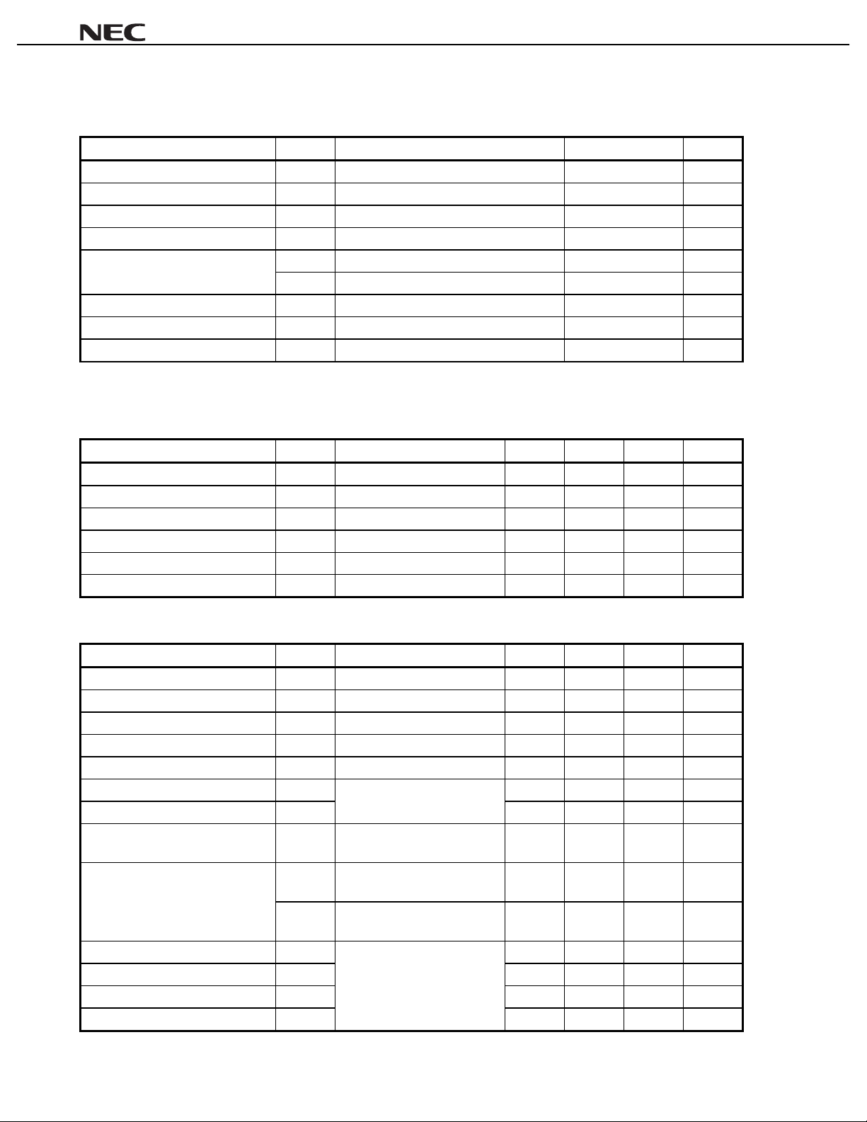
ABSOLUTE MAXIMUM RATINGS (TA = 25
When mounted on a glass epoxy board (10 cm
C)
°°°°
××××
Parameter Symbol Condition Rating Unit
Control block supply v ol t age V
Output block supply v ol tage V
Input voltage V
Output terminal voltage V
Output current
Power consumption P
Peak junction temperature T
Storage temperature range T
DD
M
IN
OUT
D(DC)
I
D(pulse)
I
T
CH(MAX)
stg
DC
PW ≤ 10 ms, Duty ≤ 5%
RECOMMENDED OPERATING CONDITIONS
When mounted on a glass epoxy board (10 cm
Parameter Symbol Condition MIN. TYP. MAX. Unit
Control block supply v ol t age V
Output block supply v ol tage V
Output current I
Operating frequency f
Operating temperature range T
Peak junction temperature T
DD
M
D(DC)
IN
A
CH(MAX)
××××
DC
IN, EN terminal 100 kHz
10 cm
10 cm
1 mm, 15% copper foil)
××××
1 mm, 15% copper foil)
××××
2.5 5.5 V
2.7 5.5 V
0.2 +0.2 A
−
10 85
−
0.5 to +6.0 V
−
0.5 to +6.0 V
−
DD
0.5 to V
−
+ 0.5 V
6.2 V
0.3 A/ch
±
0.7 A/ch
±
0.7 W
150
55 to +150
−
125
C
°
C
°
C
°
C
°
CHARACTERISTICS (Unless otherwise specified, VDD = VM = 3 V, TA = 25
Parameter Symbol Condition MIN. TYP. MAX. Unit
Off state VM pin current I
VDD pin current I
High level input current I
Low level input current I
Input pull down resistance R
High level input voltage V
Low level input voltage V
H-bridge ON resistance R
Low voltage malfunction
prevention circuit operati ng voltage
H bridge output turn-on time t
H bridge output turn-off time t
H bridge output rise time t
H bridge output fall time t
M(OFF)
DD
IH
IL
IND
IH
IL
ON
DDS1
V
DDS2
V
ONH
OFFH
r
f
All control terminal: L l evel 10
All control terminal: L l evel 10
DD
VIN = V
VIN = 0 V
1.0
−
50 200 k
DD
2.5 V ≤ VDD ≤ 5.5 V
0.7 × V
3.0 0.3 × V
−
2.5 V ≤ VM, VDD ≤ 5.5 V
Upper + lower
VM = 5 V
−10°C ≤
VM = 3 V
−10°C ≤
RM = 20
Figure 1
A
T
≤ +85°C
A
T
≤ +85°C
Ω
0.8 2.5 V
0.65 2.5 V
0.1 0.4 1.0
C)
°°°°
0.06 mA
VDD+0.3 V
3.0
0.7 20
0.2 0. 5
70 200 ns
A
µ
A
µ
A
µ
Ω
DD
V
Ω
s
µ
s
µ
s
µ
2
Data Sheet S13964EJ1V0DS00
Page 3
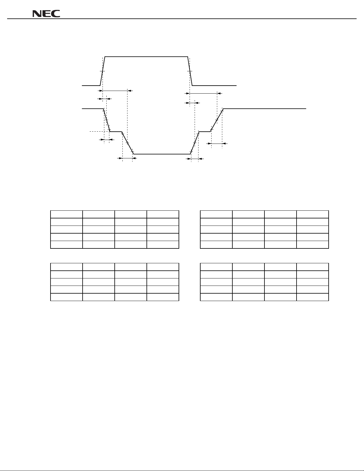
Figure 1. Switching time condition
100%
µµµµ
PD16877
50%
V
IN
50%
0%
t
ONH
t
OFFH
t
OFFH
t
ONH
100% 100%
90% 90%
50%
I
D
0%
t
10% 10%
−10%
f
−50% −50%
−90% −90%
t
r
−100%
50%
−10%
t
r
t
f
The current flowing in the direction from
A
to OUT_B is assumed to be (+).
OUT_
FUNCTION TABLE
Channel 1 Channel 2
1
EN
HLHL HLHL
HHLH HHLH
LLZZ LLZZ
LHZZ LHZZ
IN
1
OUT
1A
OUT
1B
EN
2
IN
2
OUT
2A
OUT
2B
Channel 3 Channel 4
3
EN
HLHL HLHL
HHLH HHLH
LLZZ LLZZ
LHZZ LHZZ
IN
3
OUT
3A
OUT
3B
EN
4
IN
4
OUT
4A
OUT
H: High-level, L: Low-level, Z: High impedance
4B
Data Sheet S13964EJ1V0DS00
3
Page 4
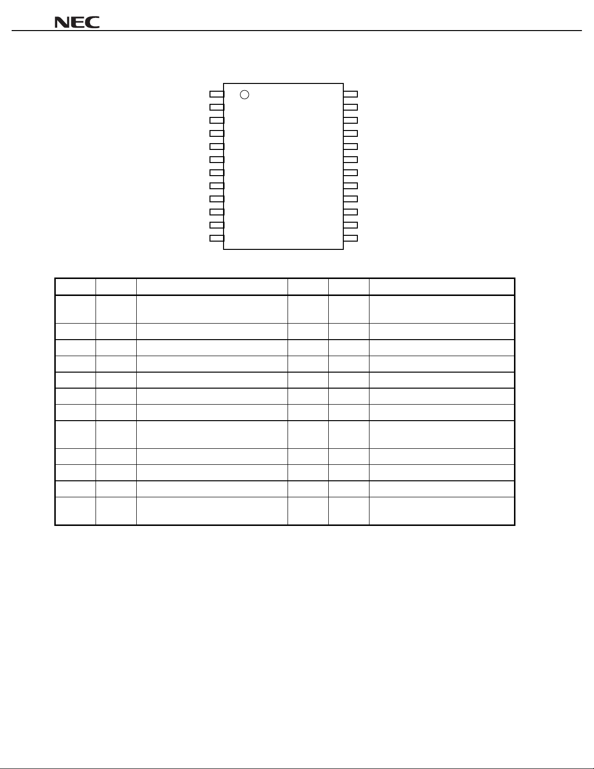
PIN CONNECTION
µµµµ
PD16877
V
OUT
PGND
OUT
OUT
PGND
OUT
V
IN
EN
IN
EN
M1
1
1A
2
3
2A
4
3A
5
6
4A
7
M4
8
1
9
1
10
2
11
2
12
24
23
22
21
20
19
18
17
16
15
14
13
V
DD
OUT
PGND
OUT
V
M23
OUT
PGND
OUT
EN
4
IN
4
EN
3
IN
3
1B
2B
3B
4B
Pin No. Pin name Pin function Pin No. Pin name Pin function
Output block supply v ol tage input
1V
M1
terminal
13 IN
2OUT1AOutput terminal 14 EN
3 PGND Ground terminal 15 IN
4OUT2AOutput terminal 16 EN
5OUT3AOutput terminal 17 OUT
3
Control terminal (channel 3)
3
Enable terminal (channel 3)
4
Control terminal (channel 4)
4
Enable terminal (channel 4)
4B
Output terminal
6 PGND Ground terminal 18 PGND Ground terminal
7OUT4AOutput terminal 19 OUT
Output block supply v ol tage input
8V
M4
terminal
20 V
9IN1Control terminal (channel 1) 21 OUT
10 EN
11 IN
12 EN
1
Enable terminal (channel 1) 22 PGND Ground terminal
2
Control terminal (channel 2) 23 OUT
2
Enable terminal (channel 2) 24 V
3B
Output terminal
Output block supply v ol tage input
M23
terminal
2B
Output terminal
1B
Output terminal
Control block supply v ol t age i nput
DD
terminal
4
Data Sheet S13964EJ1V0DS00
Page 5

BLOCK DIAGRAM
IN
9
EN
10
IN
11
EN
12
µµµµ
PD16877
24
V
Low volatge
DD
malfunction
prevention
circuit
V
M1
1
1
1
Control
circuit (1)
H-bridge
(1)
OUT
OUT
1A
2
1B
23
PGND
3
V
M23
20
2
2
circuit (2)
Control
H-bridge
(2)
OUT
OUT
2A
4
2B
21
13
14
15
16
IN
EN
IN
EN
PGND
22
3
Control
3
circuit (3)
H-bridge
(3)
OUT
OUT
3A
5
3B
19
PGND
6
V
M4
8
4
4
circuit (4)
Control
H-bridge
(4)
OUT
OUT
PGND
4A
7
4B
17
18
Remark
Plural terminal (V
M
, PGND) is not only 1 terminal and connect all terminals.
Data Sheet S13964EJ1V0DS00
5
Page 6

TYPICAL CHARACTERISTICS
µµµµ
PD16877
µ
Total power dissipation PT (W)
0.7
0.6
0.5
1.0
0.8
0.6
0.4
0.2
0
−10 0
T vs. TA characteristics
P
0.7W
20 40 60
Ambient temperature T
DD vs. VDD characteristics
I
178°C/W
80 100 120
A (°C)
T
control : "L"
A = 25°C
µ
OFF state VM Pin current IM (OFF) ( A)
µ
35
30
25
20
15
10
60
50
M (OFF) vs. VM characteristics
I
T
A = 25°C
control : "L"
5
0
Output block supply voltage V
IH, IIL vs. VDD characteristics
I
654321
M (V)
A = 25°C
T
VDD pin current IDD ( A)
Input voltage VIH, VIL (V)
0.4
0.3
0.2
0.1
4.0
3.0
2.0
1.0
0
Control block supply voltage V
IH, VIL vs. VDD characteristics
V
VIH, VIL
40
IH
I
30
Input current IIH IIL ( A)
20
10
IIL
654321
DD (V)
T
A = 25°CTA = 25°C
0
Control block supply voltage V
DDS vs. VM characteristics
V
654321
DD (V)
2.0
VDD (L H)
1.5
VDD (H L)
1.0
0.5
Low voltage detection voltage VDDS (V)
00
Control block supply voltage VDD (V)
6
654321
Data Sheet S13964EJ1V0DS00
654321
Output block supply voltage VM (V)
Page 7

µµµµ
PD16877
t
ONH
, t
OFFH
RON vs. VM characteristics
vs. VM characteristics
1.0
T
A
TA = 25°C
µ
3.0
(Ω)
ON
2.5
µ
( s)
ONH
( s)
OFFH
0.8
t
ONH
= 25°C
2.0
1.5
1.0
H-bridge ON resistance R
0.5
0
Output block supply voltage V
1.0
µ
0.8
µ
( s)
r
( s)
f
0.6
0.1
t
r
, tf vs. VM characteristics
t
r
654321
M
(V)
TA = 25°C
0.6
0.4
t
OFFH
0.2
H-bridge Output turn-on time t
H-bridge Output turn-off time t
0
Output block supply voltage V
M
654321
(V)
H-bridge Output rise time t
H-bridge Output fall time t
0.2
0
Output block supply voltage V
t
f
654321
M
(V)
Data Sheet S13964EJ1V0DS00
7
Page 8

STANDARD CONNECTION EXAMPLE
VDD = VM = 2.7 V to 5.5 V
DC/DC CONVERTER
1 to 10 F
µ
µµµµ
1 to 10 F
µ
PD16877
CPU
VDD
IN1
EN1
IN2
EN2
IN3
EN3
IN4
EN4
control
circuit
low voltage
malfunction
prevention
circuit
level
shift
circuit
VM4
V
H-bridge
(1)
H-bridge
(2)
H-bridge
(3)
H-bridge
(4)
M4VM2 3
PGND
OUT1A
OUT1B
PGND
OUT
PGND
OUT
OUT3B
PGND
OUT
OUT4B
motor1
2A
OUT2B
3A
motor2
4A
8
Data Sheet S13964EJ1V0DS00
Page 9

PACKAGE DIMENSION
24-PIN PLASTIC TSSOP (5.72 mm (225))
µµµµ
PD16877
24
13
detail of lead end
F
G
R
P
L
S
1
A
A'
12
E
H
I
J
S
C
K
SN
DM
NOTE
Each lead centerline is located within 0.10 mm of
its true position (T.P.) at maximum material condition.
M
B
ITEM MILLIMETERS
A
6.65±0.10
6.5±0.1
A'
0.575
B
0.5 (T.P.)
C
0.22±0.05
D
0.1±0.05
E
F
1.2 MAX.
1.0±0.05
G
6.4±0.1
H
I
4.4±0.1
1.0±0.1
J
0.145±0.025
K
L
0.5
0.10
M
0.08
N
P3°
R
S 0.6±0.15
+5°
−3°
0.25
S24MA-50-6A5
Data Sheet S13964EJ1V0DS00
9
Page 10

RECOMMENDED SOLDERING CONDITIONS
Solder this product under the following recommended conditions.
For soldering methods and conditions other than those recommended, consult NEC.
µµµµ
PD16877
For details of the recommended soldering conditions, refer to information document
Mounting Technology Manual”
Soldering Method Soldering Conditions
Package peak temperature: 235°C; Time: 30 secs. max. (210°C min.);
Infrared reflow
VPS
Wave soldering
Number of times: 3 tim es max; Number of day: none;
Flux: Rosin-based flux wi th little chlorine cont ent (chlorine: 0.2Wt% max.) is
recommended.
Package peak temperature: 215°C; Time: 40 secs. max. (200°C min.);
Number of times: 3 tim es max.; Number of day: none;
Flux: Rosin-based flux wi th little chlorine cont ent (chlorine: 0.2 Wt% max.) is
recommended.
Package peak temperature: 260°C; Time: 10 secs. max.;
Preheating temperature: 120°C max.; Number of tim e s: once;
Flux: Rosin-based flux wi th little chlorine cont ent (chlorine: 0.2 Wt% max.) is
recommended.
.
Caution Do not use two or more soldering methods in combination.
“Semiconductor Device
Recommended
Condition Symbol
IR35-00-3
VP15-00-3
WS60-00-1
10
Data Sheet S13964EJ1V0DS00
Page 11

NOTES FOR CMOS DEVICES
1 PRECAUTION AGAINST ESD FOR SEMICONDUCTORS
Note:
Strong electric field, when exposed to a MOS device, can cause destruction of the gate oxide and
ultimately degrade the device operation. Steps must be taken to stop generation of static electricity
as much as possible, and quickly dissipate it once, when it has occurred. Environmental control
must be adequate. When it is dry, humidifier should be used. It is recommended to avoid using
insulators that easily build static electricity. Semiconductor devices must be stored and transported
in an anti-static container, static shielding bag or conductive material. All test and measurement
tools including work bench and floor should be grounded. The operator should be grounded using
wrist strap. Semiconductor devices must not be touched with bare hands. Similar precautions need
to be taken for PW boards with semiconductor devices on it.
2 HANDLING OF UNUSED INPUT PINS FOR CMOS
Note:
No connection for CMOS device inputs can be cause of malfunction. If no connection is provided
to the input pins, it is possible that an internal input level may be generated due to noise, etc., hence
causing malfunction. CMOS devices behave differently than Bipolar or NMOS devices. Input levels
of CMOS devices must be fixed high or low by using a pull-up or pull-down circuitry. Each unused
DD
pin should be connected to V
being an output pin. All handling related to the unused pins must be judged device by device and
related specifications governing the devices.
or GND with a resistor, if it is considered to have a possibility of
µµµµ
PD16877
3 STATUS BEFORE INITIALIZATION OF MOS DEVICES
Note:
Power-on does not necessarily define initial status of MOS device. Production process of MOS
does not define the initial operation status of the device. Immediately after the power source is
turned ON, the devices with reset function have not yet been initialized. Hence, power-on does
not guarantee out-pin levels, I/O settings or contents of registers. Device is not initialized until the
reset signal is received. Reset operation must be executed immediately after power-on for devices
having reset function.
Data Sheet S13964EJ1V0DS00
11
Page 12

µµµµ
PD16877
• The information in this document is subject to change without notice. Before using this document, please
confirm that this is the latest version.
• No part of this document may be copied or reproduced in any form or by any means without the prior written
consent of NEC Corporation. NEC Corporation assumes no responsibility for any errors which may appear in
this document.
• NEC Corporation does not assume any liability for infringement of patents, copyrights or other intellectual property
rights of third parties by or arising from use of a device described herein or any other liability arising from use
of such device. No license, either express, implied or otherwise, is granted under any patents, copyrights or other
intellectual property rights of NEC Corporation or others.
• Descriptions of circuits, software, and other related information in this document are provided for illustrative
purposes in semiconductor product operation and application examples. The incorporation of these circuits,
software, and information in the design of the customer's equipment shall be done under the full responsibility
of the customer. NEC Corporation assumes no responsibility for any losses incurred by the customer or third
parties arising from the use of these circuits, software, and information.
• While NEC Corporation has been making continuous effort to enhance the reliability of its semiconductor devices,
the possibility of defects cannot be eliminated entirely. To minimize risks of damage or injury to persons or
property arising from a defect in an NEC semiconductor device, customers must incorporate sufficient safety
measures in its design, such as redundancy, fire-containment, and anti-failure features.
• NEC devices are classified into the following three quality grades:
"Standard", "Special", and "Specific". The Specific quality grade applies only to devices developed based on a
customer designated "quality assurance program" for a specific application. The recommended applications of
a device depend on its quality grade, as indicated below. Customers must check the quality grade of each device
before using it in a particular application.
Standard: Computers, office equipment, communications equipment, test and measurement equipment,
audio and visual equipment, home electronic appliances, machine tools, personal electronic
equipment and industrial robots
Special: Transportation equipment (automobiles, trains, ships, etc.), traffic control systems, anti-disaster
systems, anti-crime systems, safety equipment and medical equipment (not specifically designed
for life support)
Specific: Aircraft, aerospace equipment, submersible repeaters, nuclear reactor control systems, life
support systems or medical equipment for life support, etc.
The quality grade of NEC devices is "Standard" unless otherwise specified in NEC's Data Sheets or Data Books.
If customers intend to use NEC devices for applications other than those specified for Standard quality grade,
they should contact an NEC sales representative in advance.
M7 98. 8
 Loading...