

Page 1
DATA SHEET
MOS INTEGRATED CIRCUIT
µµµµ
PD16856
MONOLITHIC CD-ROM 3-PHASE SPINDLE MOTOR DRIVER
The µPD16856 is a CD-ROM 3-phase spindle motor driver consisting of a CMOS controller and MOS bridge
outputs.
By employing 3-phase full-wave PWM as the drive method and MOS FETs at the output stage, it has been
possible to reduce the power consumption of the µPD16856 ever further than the conventional linear drive drivers
that use bipolar transistors.
By using a 30-pin shrink SOP package, a more compact-size has been achieved.
FEATURES
• Supply voltage for controller block: 5 V, supply voltage for output block: 12 V
3 V input available for the input interface
• Low on-state resistance (total on-state resistance of upper and lower MOS FETs) RON = 1.3 Ω (TYP.)
• Low power consumption due to 3-phase full-wave PWM drive method
• On-chip hole bias switch (linked with STB pin)
• On-chip IND (FG) pulse switching function, 1-phase output or 3-phase composite output
• START/STOP pin included, acting as a brake during STOP
• Standby pins included, turning off internal circuit in standby
• Low current consumption: IDD = 3 mA (Max.), IDD
• On-chip thermal shutdown circuit
• On-chip current limiting circuit; reference voltage can be set externally
• On-chip low voltage malfunction prevention circuit
• On-chip reverse rotation prevention circuit
• 30-pin plastic shrink SOP (300 mil)
ORDERING INFORMATION
Part Number Package
µ
PD16856GS 30-pin shrink SOP (0.8-mm pi t ch, 300 mil)
(ST)
= 1 µA (Max.)
Document No. S13447EJ1V0DS00 (1st edition)
Date Published April 1999 N CP(K)
Printed in Japan
The information in this document is subject to change without notice.
©
1999
Page 2
µµµµ
PD16856
ABSOLUTE MAXIMUM RATINGS (TA = 25
Parameter Symbol Conditions Ratings Unit
DD
Supply voltage
Input voltage V
Instantaneous output c urrent
Power consumption
Note 2
Note 1
Peak channel temperature T
Storage temperature range T
Notes 1.
Allowable current per phase while on-board
When mounted on glass epoxy board (100 mm × 100 mm × 1 mm)
2.
V
M
V
IN
DR (pulse)
I
T
P
CH (MAX)
stg
RECOMMENDED OPERATING RANGE
Parameter Symbol Conditions MIN. TYP. MAX. Unit
DD
V
M
V
Output current (DC) I
Instantaneous output c urrent IDR
Hole bias current I
IND pin output current I
CL pin input voltage V
Operating temperature
range
DR (DC)
HB
FG
CL
A
T
(pulse)
PW ≤ 5 ms, Duty ≤ 10%
C)
°°°°
PW ≤ 5 ms, Duty ≤ 30%
0.5 to +6.0 V
−
0.5 to +13.5 V
−
DD
0.5 to V
−
+ 0.5 V
2.0 A/phase
±
1.0 W
150
55 to +150
−
4.5 5.0 5.5 VSupply voltage
10.8 12.0 13.2 V
0.5 A/Phase
±
1.5 A/Phase
±
10 15 mA
0
2.5
±
5mA
±
0.1 0.4 V
20 75
−
C
°
C
°
C
°
2
Data Sheet S13447EJ1V0DS00
Page 3
µµµµ
PD16856
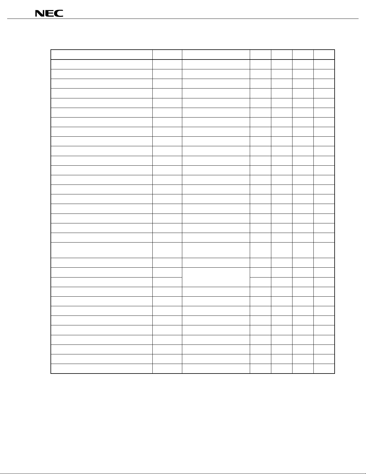
ELECTRICAL SPECIFICATIONS (UNLESS OTHERWISE SPECIFIED, TA = 25
C, VDD = 5 V, VM = 12 V)
°°°°
Parameter Symbol Conditions MIN. TYP. MAX. Unit
[General]
Current consumption 1 (during operation) I
DD
Current consumption (in standby) IDD
(ST)
STB = V
STB = GND 1.0
DD
1.5 3.0 mA
[ST/SP, STB, REV, FGsel]
Input voltage, high V
Input voltage, low V
Input pull-down resistor R
IH
IL
IND
1.8 V
120 k
DD
0.8 V
[Controller block]
Triangle wave oscillation frequency f
PWM
CT = 100 pF 75 kHz
[Hole amplifier]
Common mode input voltage range V
Hysteresis volt age V
Input bias current I
Hch
Hhys
Hbias
1.0 3.5 V
VH = 2.5 V 15 mV
1.0
[Hole bias block]
Hole bias voltage V
HB
IHB = 10 mA 0.3 0.5 V
[FG output]
IND-pin voltage, high V
IND-pin voltage, low V
FG_H
FG_L
IFG = −2.5 mA 4.0 V
IFG = +2.5 mA 0.5 V
[Output block]
Output on-state resistance (upper stage +
lower stage)
Leakage current during OFF IDR
Output turn-on time t
Output turn-off time t
R
ONH
OFFH
ON
(OFF)
IDR = 200 mA
A
T
= −20°C to +75°C
1.3 1.8
In standby 10
RM = 5
Ω
Star connection
1.0 2.0
1.0 2.0
[Torque command]
Control reference input voltage range ECR 0.3 4.0 V
Control input voltage range EC 0.3 4.0 V
Input current I
Input voltage differenc e ECR-EC
IN
Note
DUTY = 100% 1.0 V
30 50
Dead zone (+) EC_d+ 1.5 V ≤ ECR ≤ 2.5 V 0 50 100 mV
Dead zone (−)EC_d
1.5 V ≤ ECR ≤ 2.5 V 0
−
50
−
100 mV
−
[Overcurrent detection bl ock]
Input offset volt age V
IO
15 +15 mV
−
A
µ
V
Ω
A
µ
Ω
A
µ
s
µ
s
µ
A
µ
Dead zone not included.
Note
Remarks 1.
The thermal shutdown circuit (T.S.D.) operates with T
The low-voltage malfunction prevention circuit (UVLO) operates with a voltage of 4 V
2.
CH
> 150°C.
Data Sheet S13447EJ1V0DS00
TYP
.
3
Page 4
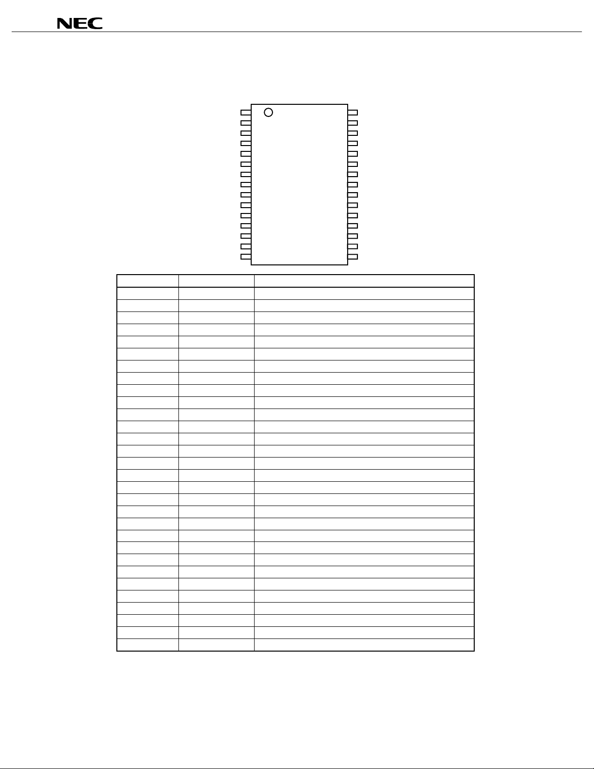
PIN FUNCTIONS
Package: 30-pin Shrink SOP (300 mil)
µµµµ
PD16856
IND
STB
V
V
OUT2
RF
RF
OUT1
V
V
OUT0
RF
RF
SEN
I
CL
1
2
3
M
4
M
5
6
7
8
9
M
10
M
11
12
13
14
15
30
29
28
27
26
25
24
23
22
21
20
19
18
17
16
EC
ECR
DD
V
CT
H2+
H2–
H1+
H1–
H0+
H0–
HB
FGsel
ST/SP
REV
GND
Pin No. Pin Name Pin Function
1 IND Index signal out put pin
2 STB Standby operation input pin
3V
4V
M
M
Supply input pin for motor block (12 V)
Supply input pin for motor block (12 V)
5 OUT2 Motor connection pin
6 RF 3-phase bridge common pin
7 RF 3-phase bridge common pin
8 OUT1 Motor connection pin
9V
10 V
M
M
Supply input pin for motor block (12 V)
Supply input pin for motor block (12 V)
11 OUT0 Motor connection pin
12 RF 3-phase bridge common pin
13 RF 3-phase bridge common pin
14 I
SEN
Sense resistor connection pin
15 CL Overcurrent detection voltage input pin
16 GND GND pin
17 REV Reverse rotation input pin (reverse brake pin)
18 ST/SP Start/stop input pin
19 FGsel IND pulse selection pin
20 HB Hole bias pin
21 H0
−
Hole signal input pin
22 H0+ Hole signal input pin
23 H1
−
Hole signal input pin
24 H1+ Hole signal input pin
25 H2
−
Hole signal input pin
26 H2+ Hole signal input pin
27 CT Oscillation frequency setup c apacitor connection pin
28 V
DD
Controller block supply i nput pi n (5 V)
29 ECR Control reference voltage input pi n
30 EC Control voltage input pin
Caution When there is more than one pin of the same kind of pin (VM and RF), all pins should be connected
to their targets.
4
Data Sheet S13447EJ1V0DS00
Page 5
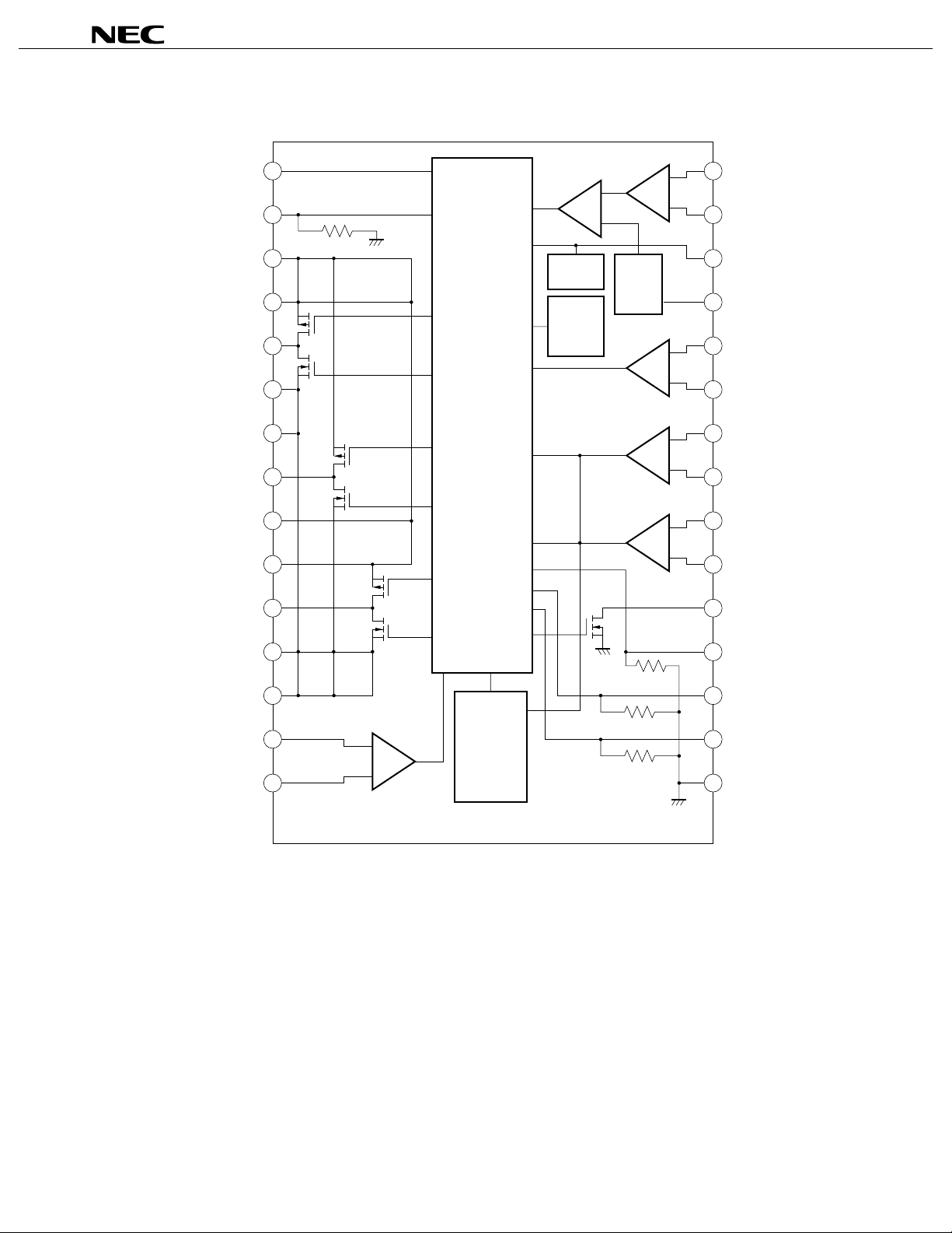
BLOCK DIAGRAM
µµµµ
PD16856
IND
STB
V
V
OUT2
RF
RF
OUT1
V
V
OUT0
RF
1
2
M
3
M
4
Q5
5
UVLO
T.S.D
OSC
+
30
29
28
27
26
EC
ECR
V
DD
C
T
H2+
Q6
6
Phase
–
25
H2–
excitation
pulse
7
generator
+
24
H1+
Q3
8
–
23
H1–
Q4
M
9
M
10
+
–
22
21
H0+
H0–
Q1
11
12
Q2
Ganged
with STB
20
19
HB
FGsel
I
RF
SEN
13
14
Reverse
rotation
18
17
ST/SP
REV
detection
CL
15
circuit
16
GND
Caution When there is more than one pin of the same kind of pin (VM and RF), all pins should be connected
to their targets.
Data Sheet S13447EJ1V0DS00
5
Page 6

TOTAL POWER DISSIPATION VS. AMBIENT TEMPERATURE CHARACTERISTICS
P
T
vs. TA Characteristics
1.4
While mounted on a 100 mm ×
100 mm × 1.0 mm glass epoxy board
1.2
µµµµ
PD16856
Remark
(W)
T
1.0
0.8
0.6
Total power dissipation P
0.4
0.2
0
–20 0 25 50 75 100 125 150
1.0 W
25˚C
125˚C/W
Ambient temperature T
75˚C
A
(˚C)
It is possible to apply a maximum of 1 W of power when the ambient temperature is 25°C or lower.
When the ambient temperature is higher than 25°C, derate based on the above chart.
It is possible to apply 0.6 W to the IC when the ambient temperature is 75°C, which is within recommended
ambient temperature conditions.
6
Data Sheet S13447EJ1V0DS00
Page 7

µµµµ
PD16856
STANDARD CHARACTERISTICS CURVES (UNLESS OTHERWISE SPECIFIED, TA = 25
IDD and IDD (ST) vs. VDD Characteristics
2.0
µ
1.0
Circuit current IDD (mA)
Circuit current in standby IDD (ST) ( A)
0
4.5 5.0 5.5
Controller block supply voltage VDD (V) Controller block supply voltage VDD (V)
2.0
IDD
IDD (ST)
VIH and VIL vs. VDD Characteristics
(ST/SP, REV, STB, and FGsel pins)
IIN vs. VDD Characteristics (EC and ECR pins)
50
µ
40
30
20
10
Torque command block input current IIN ( A)
0
4.5 5.0 5.5
20
IIN
VHhys vs. VDD Characteristics
(Hole Amplifier Input)
C)
°°°°
EC, ECR = 4 V
VH = 2.5 V
IL (V)
1.5
VIH
Input voltage, high VIH (V)
Input voltage, low V
1.0
4.5 5.0 5.5
100
50
PWM oscillation frequency fPWM (kHz)
VIL
Controller block supply voltage VDD (V)
fPWM vs. VDD Characteristics
fPWM
VIL
CT = 100 pF
15
Hole amplifier hysteresis voltage VHhys (mV)
10
4.5 5.0 5.5
Controller block supply voltage VDD (V)
RON vs. TA Characteristics
1.5
1.0
Output on-state resistance RON (Ω)
VHhys
VDD = 5 V
RON
0
4.5 5.0 5.5
Controller block supply voltage VDD (V)
Data Sheet S13447EJ1V0DS00
0.5
30 40 50 60 70
Operating ambient temperature T
A (V)
7
Page 8

FUNCTION OPERATION TABLE
(1) ST/SP = “H”
Input Signal Circuit Operation Mode Source → Sink
CMP0 CMP1 CMP2 PWM
H H L H Operation
HHL LBrake
H L L H Operation
HLLLBrake
H L H H Operation
HLHLBrake
L L H H Operation
LLHLBrake
L H H H Operation
LHHLBrake
L H L H Operation
LHLLBrake
Brake: Regenerates via the high-side Pch MOS FET channel.
(2) ST/SP = “L”
Input Signal Circuit Operation Mode
CMP0 CMP1 CMP2 PWM
−−−−
Short brake
Short brake: Turns the high-side MOS FET on and the low-side MOS FET off.
W → V
W → U
V → U
V → W
U → W
U → V
µµµµ
PD16856
(3) Torque Command
The curve shown below is the relationship to torque of the difference (ECR – EC) between the control reference
voltage (ECR) and the control voltage (EC).
Duty cycle
Normal direction torque
→ ECR–EC (+)(–)
–100%
Reverse direction torque
Stops after detecting reverse rotation
Note
The reverse drive current flows in the high-side Pch
MOS FET channel on reverse rotation.
Reverse Rotation Pin Volt age (REV)
LH
ECR > EC Normal rotation Reverse rotation
ECR < EC Reverse rotation
Note
Stop
100%
Note
8
Data Sheet S13447EJ1V0DS00
Page 9

µµµµ
PD16856
(4) Standby Mode
The setting of the standby mode allows the power supply in the device to be turned off forcibly.
The status of outputs from pins in standby is high impedance (H-bridge all OFF). In addition it is possible to
reduce the circuit current since the internal oscillation block stops.
When the stop operation is executed by the standby pin during normal operation, the motor is stopped by inertia
force.
When the normal status is reset, it takes several tens of
STB Pin Operation Mode
H Normal operation mode
L Standby mode
s to be activated.
µ
Data Sheet S13447EJ1V0DS00
9
Page 10

TIMING CHART
(1) Hole Signal Input
H
0
H
1
H
2
(2) CMP Signal (FGsel = L: IND1, FGsel = H: IND2)
µµµµ
PD16856
CMP0
CMP1
CMP2
IND1
IND2
(3) Selection of Output MOS FET Drive and Comparator (A Blank Indicates Switch OFF)
Q1 SW SW ON ON SW SW ON ON
Q2 SW SW SW SW
Q3 SW ON ON SW SW ON ON SW SW
Q4 SW SW SW SW SW
Q5 ON ON SW SW ON ON SW SW ON
Q6 SW SW SW SW
10
Data Sheet S13447EJ1V0DS00
Page 11

(4) Motor Drive Waveform
PWMOUT0 PWM
µµµµ
PD16856
PWM
PWMOUT1 PWM
PWMOUT2 PWM
Data Sheet S13447EJ1V0DS00
11
Page 12

APPLICATION CIRCUIT EXAMPLE
5 V
µµµµ
PD16856
+
µµ
15 F
controller
controller
EC
ECR
30
29
DD
V
28
UVLO
200 Ω
100 pF
CTH2+
27
OSC
HW
26
T.S.D
HU
HV
CPU
CPU
CPU
200 Ω
H2–
H1+
H1–
H0+
H0–
HB
FGsel
ST/SP
REV
GND
25
24
23
22
21
20
19
18
17
16
+
–
+
–
+
–
pulse
Phase
excitation
generator
Ganged
with STB
rotation
Reverse
detection
circuit
Remark
Q1
Q2
Q4
Q3
Q5
Q6
5
6
7
RF
RF
OUT2
Motor W phase
8
9
MVM
V
OUT1
Motor V
phase
10
11
OUT0
Motor U
phase
12
RF
13
RF
1.8 kΩ
FIL
R
14
SEN
I
330 pF
S
R
15
CL
FIL
C
CL
V
0.3 V
0.3 Ω
12 V
+
47 F
1
2
IND
STB
CPU
controller
3
MVM
V
4
To eliminate noise during PWM, it is recommended to insert a tantalum capacitor between VM and GND
(47
F in the above figure).
µ
Moreover, set VCL and RS to values within the ratings.
This circuit is for reference only and is not intended for use in mass production.
12
Data Sheet S13447EJ1V0DS00
Page 13

PACKAGE DRAWING
30-Pin Plastic Shrink SOP (300 mil) (Unit: mm)
30
16
Detail of lead end
+7
-3
3˚
µµµµ
PD16856
115
1.55±0.1
1.8 MAX.
0.1±0.1
0.8
0.35
13.0 MAX.
+0.10
–0.05
0.10
+0.10
0.9 MAX.
0.10
M
–0.05
0.20
0.6±0.2
7.7±0.3
5.6±0.2
1.05±0.2
Data Sheet S13447EJ1V0DS00
13
Page 14

µµµµ
RECOMMENDED SOLDERING CONDITIONS
PD16856 should be soldered and mounted under the following recommended conditions. For soldering methods
µ
and conditions other than those recommended below, contact your NEC sales representative.
PD16856
For the details of the recommended soldering conditions, refer to the document
•
Technology Manual (C10535E)
Soldering Method Soldering Conditions Recommended
Infrared reflow Package peak temperat ure: 235°C, Time: 30 sec. Max. (at 210°C or higher),
Count: three times or less, Exposure limit: none
with little chlorine c ontent (chlorine: 0.2 Wt% Max.) is recommended
VPS Package peak temperature: 215°C, Time: 40 sec. Max. (at 200°C or higher),
Count: three times or less, Exposure limit: none
with little chlorine c ontent (chlorine: 0.2 Wt% Max.) is recommended
Wave soldering Package peak temperature: 260°C, Time: 10 sec. Max . , Proheating
temperature: 120°C Max., Count: once, Fl ux: Rosin-based flux with l i t tle
chlorine content (chlorine: 0.2 Wt% Max.) is recommended
After opening the dry pack, store it at 25°C or less and 65% RH or less for the allowable storage period.
Note
.
Note
, Flux: Rosin-based flux
Note
, Flux: Rosin-based flux
Semiconductor Device Mounting
Condition Symbol
IR35-00-3
VP15-00-3
WS60-00-1
Caution Do not use different soldering methods together.
14
Data Sheet S13447EJ1V0DS00
Page 15

µµµµ
PD16856
Regional Information
Some information contained in this document may vary from country to country. Before using any NEC
product in your application, pIease contact the NEC office in your country to obtain a list of authorized
representatives and distributors. They will verify:
•
Device availability
•
Ordering information
•
Product release schedule
•
Availability of related technical literature
•
Development environment specifications (for example, specifications for third-party tools and
components, host computers, power plugs, AC supply voltages, and so forth)
•
Network requirements
In addition, trademarks, registered trademarks, export restrictions, and other legal issues may also vary
from country to country.
NEC Electronics Inc. (U.S.)
Santa Clara, California
Tel: 408-588-6000
800-366-9782
Fax: 408-588-6130
800-729-9288
NEC Electronics (Germany) GmbH
Duesseldorf, Germany
Tel: 0211-65 03 02
Fax: 0211-65 03 490
NEC Electronics (UK) Ltd.
Milton Keynes, UK
Tel: 01908-691-133
Fax: 01908-670-290
NEC Electronics Italiana s.r.l.
Milano, Italy
Tel: 02-66 75 41
Fax: 02-66 75 42 99
NEC Electronics (Germany) GmbH
Benelux Office
Eindhoven, The Netherlands
Tel: 040-2445845
Fax: 040-2444580
NEC Electronics (France) S.A.
Velizy-Villacoublay, France
Tel: 01-30-67 58 00
Fax: 01-30-67 58 99
NEC Electronics (France) S.A.
Spain Office
Madrid, Spain
Tel: 91-504-2787
Fax: 91-504-2860
NEC Electronics (Germany) GmbH
Scandinavia Office
Taeby, Sweden
Tel: 08-63 80 820
Fax: 08-63 80 388
NEC Electronics Hong Kong Ltd.
Hong Kong
Tel: 2886-9318
Fax: 2886-9022/9044
NEC Electronics Hong Kong Ltd.
Seoul Branch
Seoul, Korea
Tel: 02-528-0303
Fax: 02-528-4411
NEC Electronics Singapore Pte. Ltd.
United Square, Singapore 1130
Tel: 65-253-8311
Fax: 65-250-3583
NEC Electronics Taiwan Ltd.
Taipei, Taiwan
Tel: 02-2719-2377
Fax: 02-2719-5951
NEC do Brasil S.A.
Electron Devices Division
Rodovia Presidente Dutra, Km 214
07210-902-Guarulhos-SP Brasil
Tel: 55-11-6465-6810
Fax: 55-11-6465-6829
J99.1
Data Sheet S13447EJ1V0DS00
15
Page 16

µµµµ
PD16856
No part of this document may be copied or reproduced in any form or by any means without the prior written
consent of NEC Corporation. NEC Corporation assumes no responsibility for any errors which may appear in this
document.
NEC Corporation does not assume any liability for infringement of patents, copyrights or other intellectual
property rights of third parties by or arising from use of a device described herein or any other liability arising
from use of such device. No license, either express, implied or otherwise, is granted under any patents,
copyrights or other intellectual property rights of NEC Corporation or others.
While NEC Corporation has been making continuous effort to enhance the reliability of its semiconductor devices,
the possibility of defects cannot be eliminated entirely. To minimize risks of damage or injury to persons or
property arising from a defect in an NEC semiconductor device, customers must incorporate sufficient safety
measures in its design, such as redundancy, fire-containment, and anti-failure features.
NEC devices are classified into the following three quality grades:
"Standard", "Special", and "Specific". The Specific quality grade applies only to devices developed based on
a customer designated "quality assurance program" for a specific application. The recommended applications
of a device depend on its quality grade, as indicated below. Customers must check the quality grade of each
device before using it in a particular application.
Standard: Computers, office equipment, communications equipment, test and measurement equipment,
audio and visual equipment, home electronic appliances, machine tools, personal electronic
equipment and industrial robots
Special: Transportation equipment (automobiles, trains, ships, etc.), traffic control systems, anti-disaster
systems, anti-crime systems, safety equipment and medical equipment (not specifically designed
for life support)
Specific: Aircrafts, aerospace equipment, submersible repeaters, nuclear reactor control systems, life
support systems or medical equipment for life support, etc.
The quality grade of NEC devices is "Standard" unless otherwise specified in NEC's Data Sheets or Data Books.
If customers intend to use NEC devices for applications other than those specified for Standard quality grade,
they should contact an NEC sales representative in advance.
Anti-radioactive design is not implemented in this product.
M4 96. 5
 Loading...