

Page 1
DATA SHEET
MOS INTEGRATED CIRCUIT
µ
PD16837
MONOLITHIC QUAD H BRIDGE DRIVER
DESCRIPTION
The µPD16837 is a monolithic quad H bridge driver employing power MOS FETs in the output stage. The MOS FETs
in the output stage lower the saturation voltage and power consumption as compared with conventional drivers using bipolar
transistors.
In addition, a low-voltage malfunction prevention circuit is also provided that prevents the IC from malfunctioning when
the supply voltage drops. A 30-pin plastic shrink SOP package is adopted to help create compact and slim application sets.
In the output stage H bridge circuits, two low-ON resistance H bridge circuits for driving actuators, and another two
channels for driving sled motors and loading motors are provided, making the product ideal for applications in CD-ROM
and DVD.
FEATURES
• Four H bridge circuits employing power MOS FETs
• High-speed PWM drive: Operating frequency: 120 kHz MAX.
• Low-voltage malfunction prevention circuit: Operating voltage: 2.5 V (TYP.)
• 30-pin shrink SOP (300 mil)
ORDERING INFORMATION
Part Number Package
µ
PD16837GS 30-pin plastic SSOP (300 mil)
ABSOLUTE MAXIMUM RATINGS (TA = 25 °C)
Parameter Symbol Conditions Rating Unit
Control block supply voltage VDD –0.5 to +7.0 V
Output block supply voltage VM –0.5 to +15 V
Input voltage VIN –0.5 to VDD + 0.5 V
Note 2
Note 1
IDR (pulse) PW ≤ 5 ms, Duty ≤ 30 % ±1.0 A/phase
PT 1.25 W
H bridge drive current
Power dissipation
Operating temperature range TA 0 to 75 °C
Peak junction temperature TCH (MAX) 150 °C
Storage temperature range Tstg –55 to +150 °C
Notes 1. When only one channel operates.
2. When mounted on a glass epoxy board (100 mm × 100 mm × 1 mm)
The information in this document is subject to change without notice.
Document No. S12764EJ1V0DS00 (1st edition)
Date Published January 1998 N CP(K)
Printed in Japan
©
1998
Page 2
µ
PD16837
RECOMMENDED OPERATING RANGE
Parameter Symbol MIN. TYP. MAX. Unit
Control block supply voltage VDD
Output block supply voltage VM 10.8 12.0 13.2 V
H bridge drive current IDR (pulse)
Operating frequency fO 120 kHz
Operating temperature range TA 075°C
Peak junction temperature TCH (MAX) 125 °C
Note 1
Note 2
4.0 5.0 6.0 V
–600 600 mA
Notes 1. The low-voltage malfunction prevention circuit operates when VDD is 1.5 V or higher but less than 4 V
(2.5 V TYP.).
2. PW ≤ 5 ms, Duty ≤ 10%
ELECTRICAL CHARACTERISTICS (T
A = 25 °C and the other parameters are within their recommended operating ranges as described above
T
A = 25 °C)
unless otherwise specified.
The parameters other than changes in delay time are when the current is ON.
The low-voltage malfunction prevention circuit operates when V
Parameter Symbol Conditions MIN. TYP. MAX. Unit
VM pin current (leakage current) IM VM = 13.2 V 50
VDD pin current IDD VDD = 6 V 200
High-level input current IIH VIN = VDD 0.25 mA
Low-level input current IIL VIN = 0 –2.0
Note 2
Note 2
Note 1
Note 1
VIH VDD = 5 V, VM = 12 V 3.0
VIL VDD = 5 V, VM = 12 V –0.3 0.8 V
RONa VDD = 5 V, VM = 12 V 3.0 4.0 Ω
RONb VDD = 5 V, VM = 12 V 1.5 2.0 Ω
VM = 12 V
at 100 kHz
High-level input voltage
Low-level input voltage
H bridge ON resistance (chs 2 and 3)
H bridge ON resistance (chs 1 and 4)
H bridge switching current without Isa (AVE) VDD = 5 V 3.0 mA
load (chs 2 and 3)
H bridge switching current without Isb (AVE)
load (chs 1 and 4)
DD is 1.5 V to 4 V.
VDD + 0.3
4.5 mA
µ
µ
µ
V
ch2, ch3 2A, 3A, 2B, 3B Output
Parameter Symbol Conditions MIN. TYP. MAX. Unit
Rise time tTLHa VDD = 5 V 200 ns
Rising delay time tPLHa VM = 12 V 350 ns
Change in rising delay time
Fall time tTHLa at 100 kHz 200 ns
Falling delay time tPHLa 350 ns
Change in falling delay time
∆
tPLHa 20 Ω 110 ns
∆
tPHLa 130 ns
A
A
A
ch2, ch3 2A-2B, 3A-3B
Parameter Symbol Conditions MIN. TYP. MAX. Unit
Rising delay time differential tPLHa (A-B) VDD = 5 V, VM = 12 V 50 ns
Falling delay time differential tPHLa (A-B) 20 Ω at 100kHz 50 ns
Notes 1. The input pins are the IN and SEL pins.
2. Average value of the current consumed internally by an H bridge circuit when the circuit is switched without
2
load.
Page 3
µ
PD16837
ELECTRICAL CHARACTERISTICS (TA = 25 °C)
A = 25 °C and the other parameters are within their recommended operating ranges as described above
T
unless otherwise specified.
The parameters other than changes in delay time are when the current is ON.
ch1, ch4 1A, 4A, 1B, 4B Output
Parameter Symbol Conditions MIN. TYP. MAX. Unit
Rise time tTLHb VDD = 5 V 200 ns
Rising delay time tPLHb VM = 12 V 350 ns
Change in rising delay time
∆
tPLHb 10 Ω 110 ns
Fall time tTHLb at 100 kHz 200 ns
Falling delay time tPHLb 350 ns
Change in falling delay time
∆
tPHLb 130 ns
ch1, ch4 1A-1B, 4A-4B
Parameter Symbol Conditions MIN. TYP. MAX. Unit
Rising delay time differential tPLHa (A-B) VDD = 5 V, VM = 12 V 50 ns
Falling delay time differential tPHLa (A-B) 10 Ω at 100 kHz 50 ns
PIN CONFIGURATION
Output block ch 1
Output block ch 2
IN
IN
SEL
DGND
1A
PGND1
1B
V
2A
PGND2
2B
V
IN
IN
SEL
1
1
2
2
3
1
4
5
6
7
8
M1
9
10
11
12
M2
13
3
14
4
15
2
30
29
28
27
26
25
24
23
22
21
20
19
18
17
16
SEL4
IN
8
IN
7
V
M4
4B
PGND4
4A
V
M3
3B
PGND3
3A
V
DD
SEL
3
IN
6
IN
5
Output block ch 4
Output block ch 3
3
Page 4
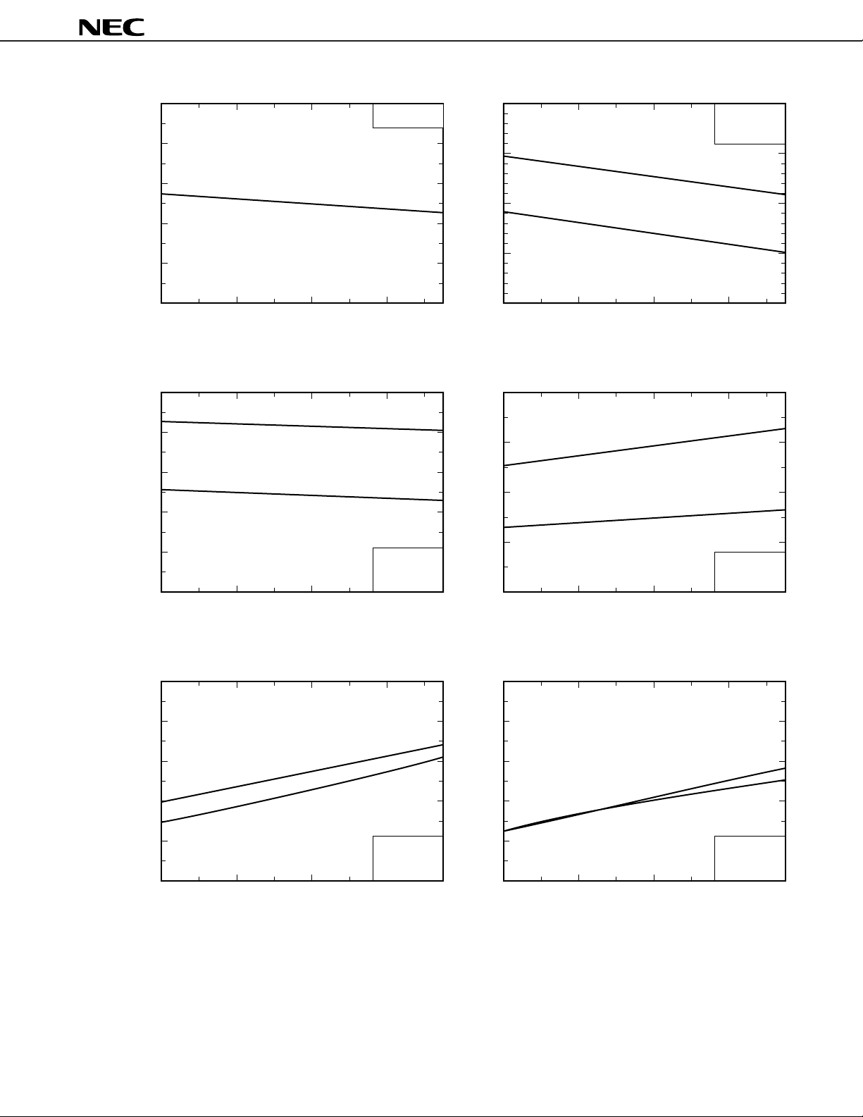
TYPICAL CHARACTERISTICS
µ
PD16837
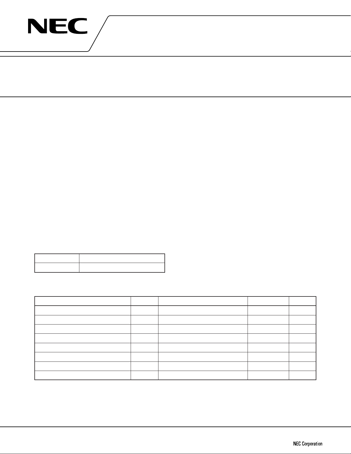
PT vs. TA Characteristics
2
(W)
T
1.25 W
1
100 °C/W
Total poser dissipation P
0
0 25 50 75 100 125 150
Ambient temperature T
IH, VIL, vs. VDD Characteristics
V
A (°C)
3
VM = 12 V
T
A
= 25 °C
(V)
IL
, V
IH
2
V
IH
V
IL
DD
vs. VDD Characteristics
I
100
80
µ
( A)
DD
60
40
Supply current I
20
0
345
Supply voltage V
ON vs. VM Characteristics
R
(Ω)
3
ON
2
V
M
= 12 V
T
A
= 25 °C
67
DD (V)
VDD = 5 V
T
A
= 25 °C
R
ONa
Input voltage V
1
Supply voltage V
DD (V)
ISa, ISb vs. VDD Characteristics
2
(mA)
Sb
, I
Sa
I
VDD = 5 V
T
A
= 25 °C
Sb
1
I
Sa
0
Switching current without load I
34567
Supply voltage V
DD (V)
R
ONb
H bridge ON resistance R
1
10 11 12 13 1434567
Motor voltage V
M (V)
IIH vs. TA Characteristics
0.2
VIN = V
(mA)
IH
0.1
High-level input current I
0
0 204060
Ambient temperature T
A (°C)
DD
4
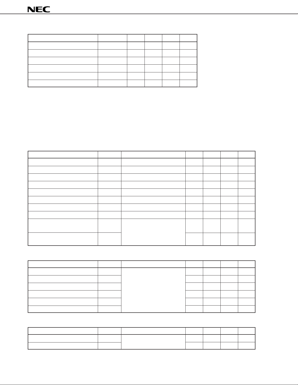
Page 5
µ
VDD = 5 V
V
M = 12 V
VDD = 5 V
V
M = 12 V
100 kHz
VDD = 5 V,
V
M = 12 V
100 kHz, 10 Ω
VDD = 5 V,
V
M = 12 V
100 kHz, 20 Ω
VDD = 5 V
V
M = 12 V
I
DD
vs. TA Characteristics
Ambient temperature T
A
(°C)
µ
VDD pin current I
DD
( A)
0 204060
100
80
60
40
20
0
I
Sa
, ISb vs. TA Characteristics
Ambient temperature T
A
(°C)
Switching current without load I
Sa
, I
Sb
(mA)
0 204060
1
0.8
0.6
0.4
0.2
0
R
ON
vs. TA Characteristics
Ambient temperature T
A
(°C)
H bridge ON resistance R
ON
(Ω)
0 204060
4
3
2
1
0
V
IH
, VIL vs. TA Characteristics
Ambient temperature T
A
(°C)
Input voltage V
IH
, V
IL
(V)
02040
V
IH
VIL
60
2
1.95
1.9
1.85
1.8
ISb
ISa
RONa
RONb
VDD = 6 V
t
TLH
, t
THL
vs. TA Characteristics (chs 1 and 4)
Ambient temperature T
A
(°C)
Rise time/fall time t
TLH
, t
THL
(ns)
0 204060
100
90
80
70
60
50
tTHL
tTLH
tTLH
tTHL
t
TLH
, t
THL
vs. TA Characteristics (chs 2 and 3)
Ambient temperature T
A
(°C)
Rise time/fall time t
TLH
, t
THL
(ns)
0 204060
100
90
80
70
60
50
PD16837
5
Page 6

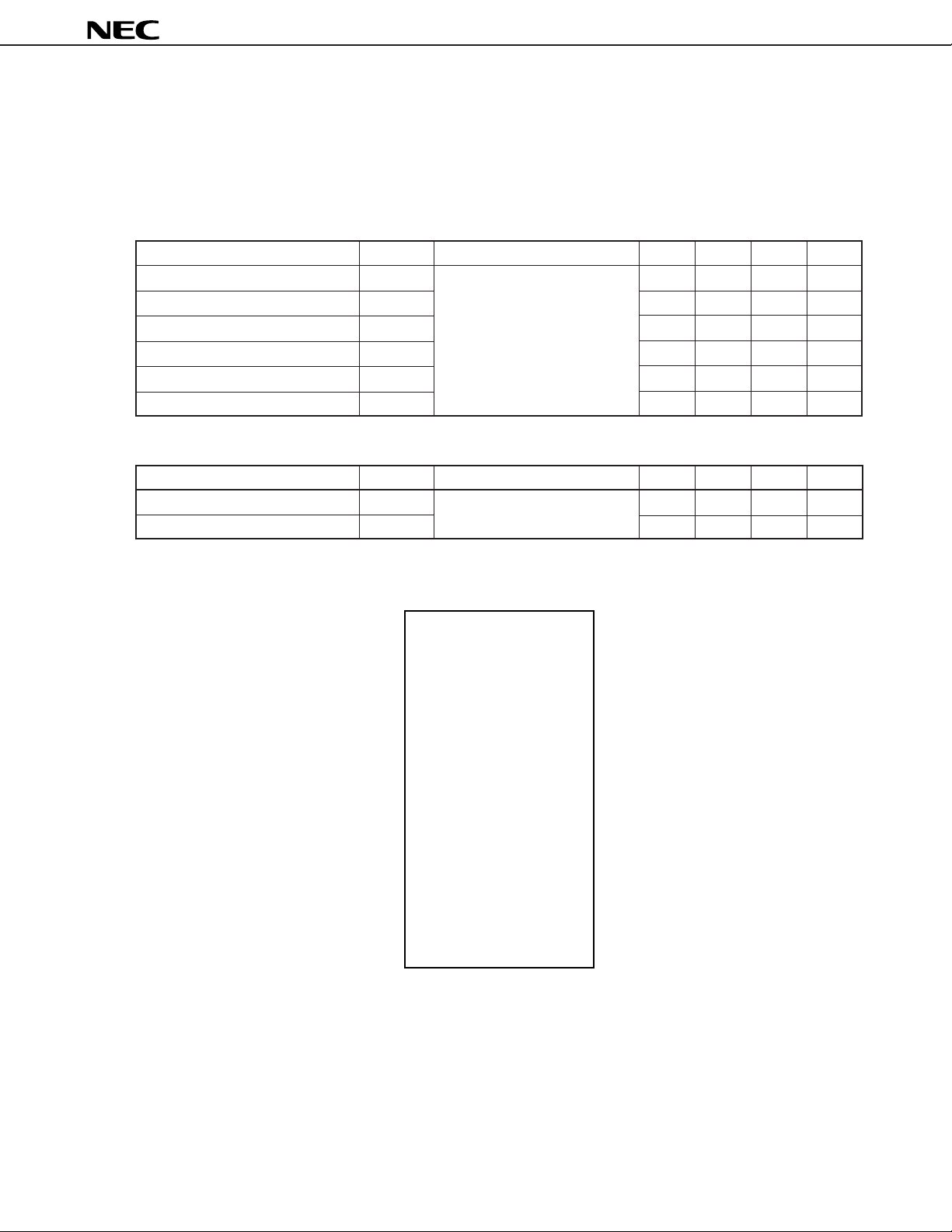
300
250
200
t
PLH
, t
PHL
vs. TA Characteristics (chs 1 and 4)
tPLH
tPHL
300
∆∆
250
200
t
PLH
, t
PHL
vs. TA Characteristics (chs 2 and 3)
µ
PD16837
t
PLH
tPHL
150
VDD = 5 V,
V
M = 12 V
A
(°C)
100 kHz, 10 Ω
100
0 204060
Rising/falling delay time (chs 1 and 4) tPLH, tPHL (ns)
Ambient temperature T
t
PLH
, t
PHL
vs. TA Characteristics (chs 1 and 4)
∆∆
100
80
∆
∆
60
40
20
0
0 204060
Rising/falling time differential (chs 1 and 4) tPLH, tPHL (ns)
Ambient temperature T
A
(°C)
VDD = 5 V,
V
M = 12 V
100 kHz, 10 Ω
PHL
t
tPLH
150
VDD = 5 V,
V
M = 12 V
100
0 204060
Rising/falling delay time (chs 2 and 3) tPLH, tPHL (ns)
100 kHz, 20 Ω
Ambient temperature TA (°C)
t
PLH
, t
PHL
∆∆
vs. TA Characteristics (chs 2 and 3)
100
tPHL
∆∆
80
60
∆
tPLH
∆
40
20
0
0 204060
Rising/falling time differential (chs 2 and 3) tPLH, tPHL (ns)
Ambient temperature T
A
(°C)
VDD = 5 V,
V
M = 12 V
100 kHz, 20 Ω
6
Page 7

PACKAGE DIMENSION
30-PIN SHRINK SOP (300 mil) (unit: mm)
µ
PD16837
30
16
115
13.0 MAX.
1.55±0.1
1.8 MAX.
0.1±0.1
0.8
0.35
+0.10
–0.05
0.10
0.9 MAX.
0.10
M
+0.10
–0.05
0.20
0.6±0.2
detail of lead end
+7°
-3°
3˚
7.7±0.3
5.6±0.2
1.05±0.2
7
Page 8

BLOCK DIAGRAM
1IN
1
2
IN
2
IN
IN
3
1
13
3
14
4
15
2
SEL
SEL
Control circuit 1
Control circuit 2
µ
PD16837
V
DD
19
8V
M1
5
1A
H bridge 1
7
1B
6
PGND
4
M2
V
2A
5
H bridge 2
26
2B
IN
IN
SEL
IN
IN
SEL
GND
6
PGND
4
M3
V
16
5
17
6
18
3
28
7
29
8
30
4
Control circuit 3
Control circuit 4
H bridge 3
H bridge 4
4
26
26
3A
5
3B
6
PGND
4
M4
V
4A
5
4B
6
PGND
LVP
Remark Connect all VM and GND pins.
: Internally pulled down to GND via 50 kΩ.
8
Page 9

FUNCTION TABLE
1, 7
IN
IN
2, 8
SEL
1, 4
VDD (common)
GND (common)
V
M1 to 4
PGND1, 4
µ
PD16837
1A, 4A (OUTA)
1B, 4B (OUTB)
IN
IN
SEL
3, 5
4, 6
2, 3
VDD (common)
GND (common)
V
M1 to 4
2A, 3A (OUTA)
2B, 3B (OUTB)
PGND2, 3
Function Table (common to all chs)
Input Output
IN1 IN2 SEL OUTA OUTB
HLHHL
LLHLL
LHHLH
HHHHH×: Don’t care
××L Z Z Z: High inpedance
9
Page 10

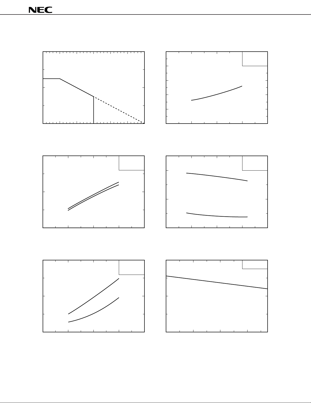
ABOUT SWITCHING
When output A is switched as shown in the figure on the right, a dead
time (time during which both P ch and N ch are OFF) elapses to prevent
through current. Therefore, the waveform of output A (rise time, fall time,
and delay time) changes depending on whether output B is fixed to the
high or low level.
The output voltage waveforms of A in response to an input waveform
where output B is fixed to the low level (1) or high level (2) are shown
below.
(1) Output B: Fixed to low level
Output A: Switching operation (Operations of P ch and N ch are shown.)
Input waveform
V
M
AB
Dead time
µ
PD16837
PchPch
NchNch
Pch:
OFF→
Nch:
ON→
Voltage waveform at point A
OFF→
OFF→
ON→
OFF→
Current ON
······ON······
······OFF······
Current OFF
OFF→
OFF→
OFF→
ON→
Output A goes into a high-impedance state and is in an undefined status during the dead time period. Because
output B is pulled down by the load, a low level is output to A.
(2) Output B: Fixed to high level
Output A: Switching operation (Operations of P ch and N ch are shown.)
Dead time
Input waveform
Pch:
OFF→
Nch:
ON→
Voltage waveform at point A
OFF→
OFF→
ON→
OFF→
Current ON
······ON······
······OFF······
OFF→
OFF→
Current OFF
OFF→
ON→
Output A goes into a high-impedance state and is in an undefined status during the dead time period. Because
output B is pulled up by the load, a high level is output to A.
10
Page 11

µ
PD16837
The switching characteristics shown on the preceding pages are specified as follows (“output at one side” means
output B for H bridge output A, or output A for output B).
[Rise time]
Rise time when the output at one side is fixed to the low level (specified on current ON).
[Fall time]
Fall time when the output at one side is fixed to the high level (specified on current ON).
[Rising delay time]
Rising delay time when the output at one side is fixed to the low level (specified on current ON).
[Falling delay time]
Falling delay time when the output at one side is fixed to the high level (specified on current ON).
[Change in rising delay time]
Change (difference) in the rising delay time between when the output at one side is fixed to the low level and when
the output at the other side is fixed to the high level.
[Change in falling delay time]
Change (difference) in falling delay time between when the output at one side is fixed to the low level and when
the output at the other side is fixed to the high level.
[Rising delay time differential]
Difference in rising delay time between output A and output B.
[Falling delay time differential]
Difference in falling delay time between output A and output B.
Caution Because this IC switches a high current at high speeds, surge may occur due to the V
GND wiring and inductance and degrade the performance of the IC.
On the PWB, keep the pattern width of the V
and insert the bypass capacitors between VM and GND at a location as close to the IC as
possible.
Connect a low-inductance magnetic capacitor (4700 pF or more) and an electrolytic capacitor
µ
of 10
F or so, depending on the load current, in parallel.
M and GND lines as wide and short as possible,
M and
11
Page 12

µ
RECOMMENDED SOLDERING CONDITIONS
Solder this product under the following recommended conditions.
For details of the recommended soldering conditions, refer to information document Semiconductor Device
Mounting Technology Manual (C10535E).
For soldering methods and conditions other than those recommended, consult NEC.
PD16837
Soldering Method Soldering Conditions
Infrared reflow
VPS
Wave soldering Package peak temperature: 260 °C; Time: 10 secs. max.; Number of WS60-00-1
Package peak temperature: 235 °C; Time: 30 secs. max. (210 °C min.);
Number of times: 3 times max.; Number of days: none
Rosin-based flux with little chlorine content (chlorine: 0.2 Wt% max.)
is recommended.
Package peak temperature: 215 °C; Time: 40 secs. max. (200 °C min.);
Number of times: 3 times max.; Number of days: none
Rosin-based flux with little chlorine content (chlorine: 0.2 Wt% max.)
is recommended.
times: once; Flux: Rosin-based flux with little chlorine content
(chlorine: 0.2 Wt% max.) is recommended.
Note
Note
; Flux:
; Flux:
Recommended
Condition Symbol
IR35-00-3
VP-15-00-3
Note Number of days in storage after the dry pack has been opened. The storage conditions are at 25 °C, 65%
RH MAX.
Caution Do not use two or more soldering methods in combination.
12
Page 13

[MEMO]
µ
PD16837
13
Page 14

[MEMO]
µ
PD16837
14
Page 15

[MEMO]
µ
PD16837
15
Page 16

µ
PD16837
No part of this document may be copied or reproduced in any form or by any means without the prior written
consent of NEC Corporation. NEC Corporation assumes no responsibility for any errors which may appear in
this document.
NEC Corporation does not assume any liability for infringement of patents, copyrights or other intellectual property
rights of third parties by or arising from use of a device described herein or any other liability arising from use
of such device. No license, either express, implied or otherwise, is granted under any patents, copyrights or other
intellectual property rights of NEC Corporation or others.
While NEC Corporation has been making continuous effort to enhance the reliability of its semiconductor devices,
the possibility of defects cannot be eliminated entirely. To minimize risks of damage or injury to persons or
property arising from a defect in an NEC semiconductor device, customers must incorporate sufficient safety
measures in its design, such as redundancy, fire-containment, and anti-failure features.
NEC devices are classified into the following three quality grades:
"Standard", "Special", and "Specific". The Specific quality grade applies only to devices developed based on a
customer designated "quality assurance program" for a specific application. The recommended applications of
a device depend on its quality grade, as indicated below. Customers must check the quality grade of each device
before using it in a particular application.
Standard: Computers, office equipment, communications equipment, test and measurement equipment,
audio and visual equipment, home electronic appliances, machine tools, personal electronic
equipment and industrial robots
Special: Transportation equipment (automobiles, trains, ships, etc.), traffic control systems, anti-disaster
systems, anti-crime systems, safety equipment and medical equipment (not specifically designed
for life support)
Specific: Aircrafts, aerospace equipment, submersible repeaters, nuclear reactor control systems, life
support systems or medical equipment for life support, etc.
The quality grade of NEC devices is "Standard" unless otherwise specified in NEC's Data Sheets or Data Books.
If customers intend to use NEC devices for applications other than those specified for Standard quality grade,
they should contact an NEC sales representative in advance.
Anti-radioactive design is not implemented in this product.
M4 96.5
2
 Loading...