

Page 1
DATA SHEET
MOS INTEGRATED CIRCUIT
µ
PD16833A
MONOLITHIC QUAD H BRIDGE DRIVER CIRCUIT
DESCRIPTION
The µPD16833A is a monolithic quad H bridge driver IC which uses power MOS FETs in its driver stage. By using the
MOS FETs in the output stage, this driver IC has a substantially improved saturation voltage and power consumption as
compared with conventional driver circuits using bipolar transistors.
A low-voltage malfunction prevention function is provided to prevent the IC from malfunctioning when the supply voltage
drops. By eliminating the charge pump circuit, the current during power-OFF is drastically decreased.
As the package, a 30-pin plastic shrink SOP is employed to enable the creation of compact, slim application sets.
This driver IC can drive two stepping motors at the same time, and is ideal for driving stepping motors in the lens of a
video camera.
FEATURES
• Four H bridge circuits employing power MOS FETs
• Low current consumption by eliminating charge pump
VM pin current when power-OFF: 10 µA MAX. VDD pin current: 10 µA MAX.
• Input logic frequency: 100 kHz
• 3-V power supply
Minimum operating supply voltage: 2.5 V
• Low-voltage malfunctioning prevention circuit
µ
• 30-pin plastic shrink SOP (300 mil) (
PD16833AG3)
ORDERING INFORMATION
Part Number Package
µ
PD16833AG3 30-pin plastic shrink SOP (300 mil)
ABSOLUTE MAXIMUM RATINGS (TA = 25 °C)
Parameter Symbol Conditions Rating Unit
Supply voltage VDD –0.5 to +6.0 V
VM –0.5 to +6.0 V
Input voltage VIN –0.5 to VDD + 0.5 V
Note 2
Note 1
IDR (DC) DC ±300 mA
Note 1
The information in this document is subject to change without notice.
IDR (pulse) PW ≤ 10 ms, Duty ≤ 5 % ±700 mA
PT 1.19 W
H bridge drive current
Instantaneous H bridge drive current
Power dissipation
Peak junction temperature TCH (MAX) 150 °C
Storage temperature range Tstg –55 to +150 °C
Notes 1. Permissible current per phase, when mounted on a printed circuit board
2. When mounted on a glass epoxy board (10 cm × 10 cm × 1 mm)
Document No. S13147EJ1V0DS00 (1st edition)
Date Published January 1998 N CP(K)
Printed in Japan
©
1998
Page 2
µ
PD16833A
Recommended Operating Conditions
Parameter Symbol MIN. TYP. MAX. Unit
Supply voltage VDD 2.5 5.5 V
VM 2.7 5.5 V
H bridge drive current IDR –200 200 mA
Logic input frequency
Operating temperature range TA –10 85 °C
Peak junction temperature TCH (MAX) 125 °C
Note
fIN 100 kHz
Note Common to IN and EN pins
DC Characteristics (Unless otherwise specified, VDD = VM = 3.0 V, TA = 25 °C)
Parameter Symbol Conditions MIN. TYP. MAX. Unit
OFF VM pin current IM (OFF) with all control pins at low level 10
VDD pin current IDD with all control pins at low level 10
High-level input current IIH VIN =VDD 0.06 mA
Low-level input current IIL VIN = 0 –1.0
Input pull-down resistor RIND 50 200 kΩ
High-level input voltage VIH VDD = 2.5 V to 5.5 V VDD × 0.7 VDD + 0.3 V
Low-level input voltage VIL VDD = 2.5 V to 5.5 V –0.3 VDD × 0.3 V
H bridge ON resistance
Low-voltage malfunction
prevention circuit operating voltage
Note
RON VDD = VM = 2.7 V to 5.5 V 3.0 Ω
VDDS1 VM = 5.0 V 0.8 2.5 V
–10 °C ≤ TA ≤ +85 °C
VDDS2 VM = 3.0 V 0.65 2.5 V
–10 °C ≤ TA ≤+85 °C
µ
A
µ
A
µ
A
Note Sum of top and bottom ON resistances (@IDR = 100 mA)
AC Characteristics (Unless otherwise specified, VDD = VM = 3.0 V, TA = 25 °C)
Parameter Symbol Conditions MIN. TYP. MAX. Unit
H bridge output circuit turn-ON tONH RM = 20 Ω, Figure 1 0.7 20
time
H bridge output circuit turn-OFF tOFFH 0.2 0.5
time
Rise time tr 0.1 0.4 1.0
Fall time tf 70 200 ns
2
µ
A
µ
A
µ
s
Page 3
µ
PD16833A
FUNCTION TABLE
Channel 1 Channel 2
EN1 IN1 OUT1A OUT1B EN2 IN2 OUT2A OUT2B
HLH L HLH L
HHL H HHL H
LLZ Z LLZ Z
LHZ Z LHZ Z
Channel 3 Channel 4
EN3 IN3 OUT3A OUT3B EN4 IN4 OUT4A OUT4B
HLH L HLH L
HHL H HHL H
LLZ Z LLZ Z
LHZ Z LHZ Z
H: High level, L: Low level, Z: High impedance IN
PIN CONFIGURATION
NC
1
NC
2
VDD
3
VM1
4
1A
5
PGND
PGND
2A
3A
4A
VM4
IN1
EN1
IN2
EN2
6
7
8
9
10
11
12
13
14
15
30
29
28
27
26
25
24
23
22
21
20
19
18
17
16
NC
NC
DGND
NC
1B
PGND
2B
VM2, 3
3B
PGND
4B
EN4
IN4
EN3
IN3
3
Page 4
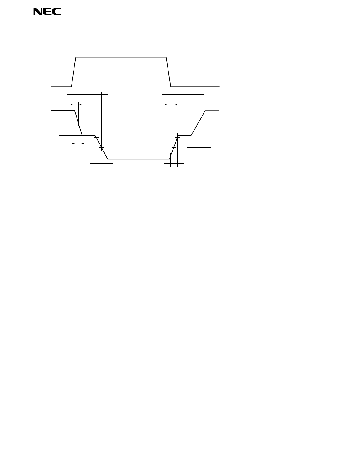
Figure 1. Switching Characteristic Wave
100 %
µ
PD16833A
V
IN
50 % 50 %
0 %
t
t
ON
t
100 %
OFF
90 %
I
DR
0 %
50 %
10 %
–10 %
t
f
–50 % –50 %
–90 % –90 %
t
r
–100 %
ON
t
OFF
100 %
90 %
50 %
10 %
–10 %
t
r
The current flowing in the direction from
OUT_A to OUT_B is assumed to be (+).
f
t
4
Page 5

BLOCK DIAGRAM
µ
PD16833A
IN
EN
EN
NC V
NCNCNCNC
DD
133029272
Low-voltage
malfunction
prevention
circuit
1
12
Control circuit
13
1
H bridge
1
DGND
14
IN
2
Control circuit
15
2
H bridge
2
26
23
24
V
M1
4
1A
5
1B
PGND
6
V
M2, 3
2A
7
2B
IN
EN
IN
EN
DGND
DGND
16
3
Control circuit
17
3
H bridge
3
DGND
18
4
Control circuit
19
4
H bridge
4
28
25
22
11
10
20
21
PGND
8
3A
3B
9
PGND
M4
V
4A
4B
PGND
5
Page 6

6
DD
= VM = 2.7 V to 5.5 V
V
STANDARD CONNECTION EXAMPLE
DC/DC Converter
µ
µ
1 to 10 F
1 to 10 F
Battery
V
M4
V
M2, 3
V
CPU
V
IN
EN
IN
EN
IN
EN
IN
EN
M1
DD
Low-voltage
H bridge 1
malfunction
1
1
2
2
Control
circuit
3
3
4
4
prevention
circuit
Level
shift
circuit
H bridge 2
H bridge 3
H bridge 4
PGND
PGND
PGND
1A
1B
Motor 1
2A
2B
3A
3B
Motor 2
4A
4B
GND
DGND
PGND
µ
PD16833A
Page 7

TYPICAL CHARACTERISTICS (TA = 25 °C)
T
vs. TA characteristics
P
1.4
1.2
1.0
(W)
T
0.8
0.6
0.4
Total power dissipation P
0.2
1.19 W
20
µ
( A)
M (OFF)
10
pin current I
M
OFF V
I
M (OFF)
vs. VM characteristics
µ
PD16833A
All control pins at
low level
T
A
= 25 °C
0
–10 0 40 60 80 100 120
Ambient temperature TA (°C) Output block supply voltage VM (V)
IIH/IIL vs. VIN characteristics
100
TA = 25 °C
80
µ
( A)
60
IL
/I
IH
IH
I
40
20
Input current I
I
0
1234
IL
Input voltage V
567
IN
(V)
0
123456
IH/VIL
vs. VDD characteristics
V
T
A
= 25 °C
3
V
(V)
IL
/V
IH
IH
V
IL
2
Input voltage V
1
1234567
Control block supply voltage VDD (V)
7
7
Page 8

200
(kΩ)
150
IND
100
Input pull-down resistor R
50
R
IND
vs. VDD characteristics
TA = 25 °C
(V)
DDS
Low voltage detection voltage V
µ
PD16833A
V
DDS
vs. VM characteristics
3
T
A
= 25 °C
2
1
0
1234 567
DD
Control block supply voltage V
(V)
RON vs. VM characteristics
3
T
A
= 25 °C
I
DR
= 100 mA
(Ω)
ON
2
1
Output ON resistor R
0
234567
1
M
Output block supply voltage V
(V)
0
1234567
M
Output block supply voltage V
R
ON
vs. TA characteristics
(V)
3
M
= 3.5 V
V
I
DR
= 100 mA
(Ω)
ON
2
1
Output ON resistor R
0
–25 0 25 50 75 100
A
Ambient temperature T
(°C)
8
Page 9

µ
PD16833A
Switching time vs. VDD/VM characteristics
1000
800
(ns)
f
/t
r
/t
600
OFF
/t
ON
400
200
Switching time t
0
123456
Supply voltage VDD/VM (V)
RM = 20 Ω
T
A
= 25 °C
ON
t
t
OFF
t
r
t
f
Switching time vs. TA characteristics
1000
DD
= VM = 3 V
V
R
M
= 20 Ω
800
(ns)
f
/t
r
/t
OFF
/t
ON
600
t
ON
t
r
400
t
200
Switching time t
0
7
0
–25 0 25 50 75 100
OFF
t
f
Ambient temperature TA (°C)
9
Page 10

PACKAGE DIMENSION
30 PIN PLASTIC SHRINK SOP (300 mil)
µ
PD16833A
30
115
A
G
F
E
C
D
M
M
N
NOTE
Each lead centerline is located within 0.10
mm (0.004 inch) of its true position (T.P.) at
maximum material condition.
16
detail of lead end
–3°
+7°
3°
H
I
K
B
L
ITEM MILLIMETERS INCHES
A
B
10.11 MAX.
0.51 MAX.
J
P30GS-65-300B-1
0.398 MAX.
0.020 MAX.
C
D
E
F
G
H
I
J
K
L
M
N
0.65 (T.P.)
+0.10
0.30
–0.05
0.125±0.075
2.0 MAX.
1.7±0.1
8.1±0.2
6.1±0.2
1.0±0.2
+0.10
0.15
–0.05
0.5±0.2
0.10
0.10
0.026 (T.P.)
+0.004
0.012
–0.003
0.005±0.003
0.079 MAX.
0.067±0.004
0.319±0.008
0.240±0.008
+0.009
0.039
–0.008
+0.004
0.006
–0.002
+0.008
0.020
–0.009
0.004
0.004
10
Page 11

µ
PD16833A
RECOMMENDED SOLDERING CONDITIONS
It is recommended to solder this product under the conditions described below.
For soldering methods and conditions other than those listed below, consult NEC.
For the details of the recommended soldering conditions of this type, refer to the Semiconductor Device Mounting
Technology Manual (C10535E).
Soldering Method Soldering Conditions
Infrared reflow
VPS
Wave soldering
Peak package temperature: 235 °C, Time: 30 seconds MAX. (210 °C MIN.),
Number of times: 3 MAX., Number of days: None
flux with little chlorine content (chlorine: 0.2 Wt% MAX.) is recommended.
Peak package temperature: 215 °C, Time: 40 seconds MAX. (200 °C MIN.),
(200 °C MIN.), Number of times: 2 MAX., Number of days: None
Flux: Rosin-based flux with little chlorine content (chlorine: 0.2 Wt% MAX.)
is recommended.
Soldering bath temperature: 260 °C MAX., Time: 10 seconds MAX.,
Preheating temperature: 120 °C MAX.,
Number of times: 1, Flux: Rosin-based flux with little chlorine content
(chlorine: 0.2 Wt% MAX.) is recommended.
Note
, Flux: Rosin-based
Note
,
Note The number of storage days at 25 °C, 65% RH after the dry pack has been opened
Caution Do not use two or more soldering methods in combination.
Symbol of Recommended
Soldering
IR35-00-3
VP15-00-2
WS60-00-1
11
Page 12

µ
PD16833A
No part of this document may be copied or reproduced in any form or by any means without the prior written
consent of NEC Corporation. NEC Corporation assumes no responsibility for any errors which may appear in
this document.
NEC Corporation does not assume any liability for infringement of patents, copyrights or other intellectual property
rights of third parties by or arising from use of a device described herein or any other liability arising from use
of such device. No license, either express, implied or otherwise, is granted under any patents, copyrights or other
intellectual property rights of NEC Corporation or others.
While NEC Corporation has been making continuous effort to enhance the reliability of its semiconductor devices,
the possibility of defects cannot be eliminated entirely. To minimize risks of damage or injury to persons or
property arising from a defect in an NEC semiconductor device, customers must incorporate sufficient safety
measures in its design, such as redundancy, fire-containment, and anti-failure features.
NEC devices are classified into the following three quality grades:
"Standard", "Special", and "Specific". The Specific quality grade applies only to devices developed based on a
customer designated "quality assurance program" for a specific application. The recommended applications of
a device depend on its quality grade, as indicated below. Customers must check the quality grade of each device
before using it in a particular application.
Standard: Computers, office equipment, communications equipment, test and measurement equipment,
audio and visual equipment, home electronic appliances, machine tools, personal electronic
equipment and industrial robots
Special: Transportation equipment (automobiles, trains, ships, etc.), traffic control systems, anti-disaster
systems, anti-crime systems, safety equipment and medical equipment (not specifically designed
for life support)
Specific: Aircrafts, aerospace equipment, submersible repeaters, nuclear reactor control systems, life
support systems or medical equipment for life support, etc.
The quality grade of NEC devices is "Standard" unless otherwise specified in NEC's Data Sheets or Data Books.
If customers intend to use NEC devices for applications other than those specified for Standard quality grade,
they should contact an NEC sales representative in advance.
Anti-radioactive design is not implemented in this product.
M4 96.5
2
 Loading...