

Page 1
DATA SHEET
MOS INTEGRATED CIRCUIT
µ
PD16814
MONOLITHIC DUAL H BRIDGE DRIVER CIRCUIT
DESCRIPTION
The µPD16814GS is a monolithic dual H bridge driver circuit employing a power MOS FET for its driver stage. By
complementing the P channel and N channel of the output stage, the circuit current is substantially improved as
compared with that of the conventional charge pump driver.
Because the dual H bridge driver circuits at the output stage are independent of each other, this IC is ideal as the
driver circuit for a 1- to 2-phase excitation bipolar driving stepping motor for the head actuator of an FDD.
FEATURES
• Low ON resistance (sum of ON resistance of top and bottom FETs)
ON1 = 2.0 Ω TYP.
R
• Low current consumption: IDD = 100 µA MAX.
• Four input modes independently controlling dual H bridge drivers
• Stop and Brake modes selectable
• Surface-mount mini-mold package: 16-pin plastic SOP (300 mil)
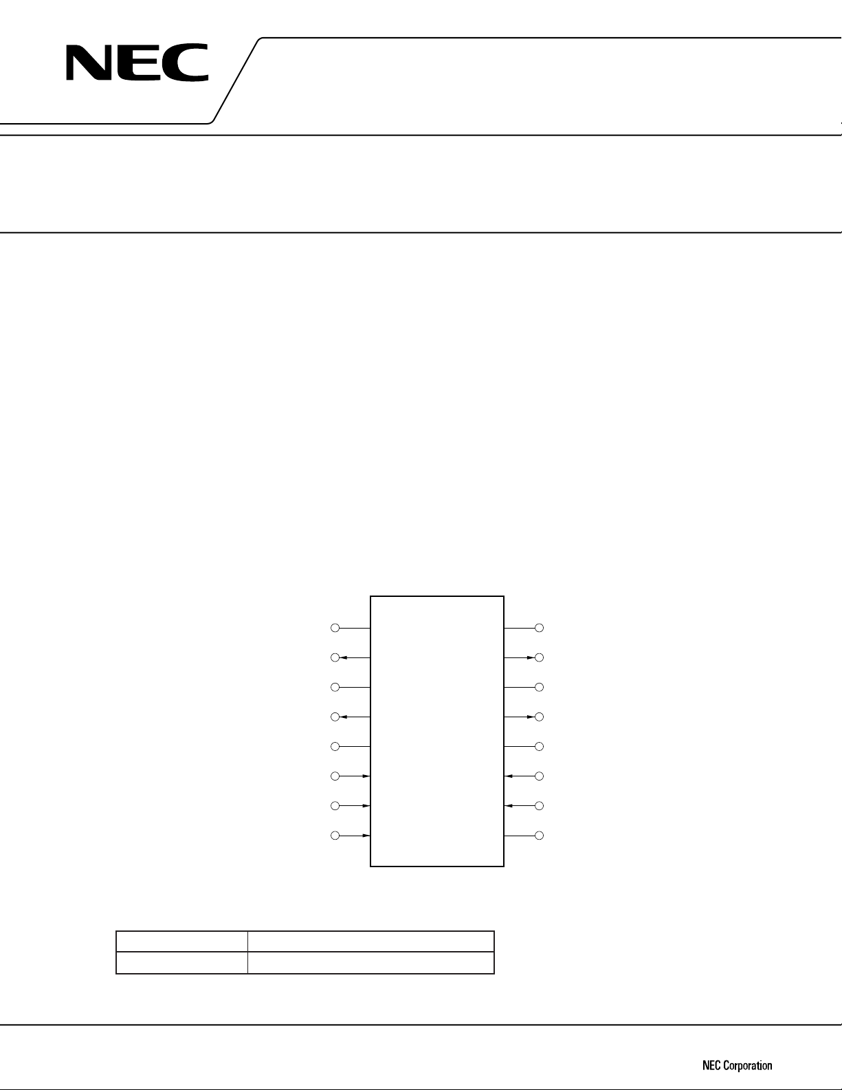
PIN CONFIGURATION (Top View)
V
M1
1A
PGND
1
2A
V
DD
IN
1
IN
3
IN
2
ORDERING INFORMATION
Part Number Package
µ
PD16814GS 16-pin plastic SOP (300 mil)
1
2
3
4
5
6
7
8
µ
PD16814GS
16
15
14
13
12
11
10
9
NC
1B
PGND
2B
V
M2
SEL
IN
4
DGND
2
The information in this document is subject to change without notice.
Document No. S10112EJ4V0DS00 (4th edition)
Date Published August 1997 N
Printed in Japan
©
1997
Page 2
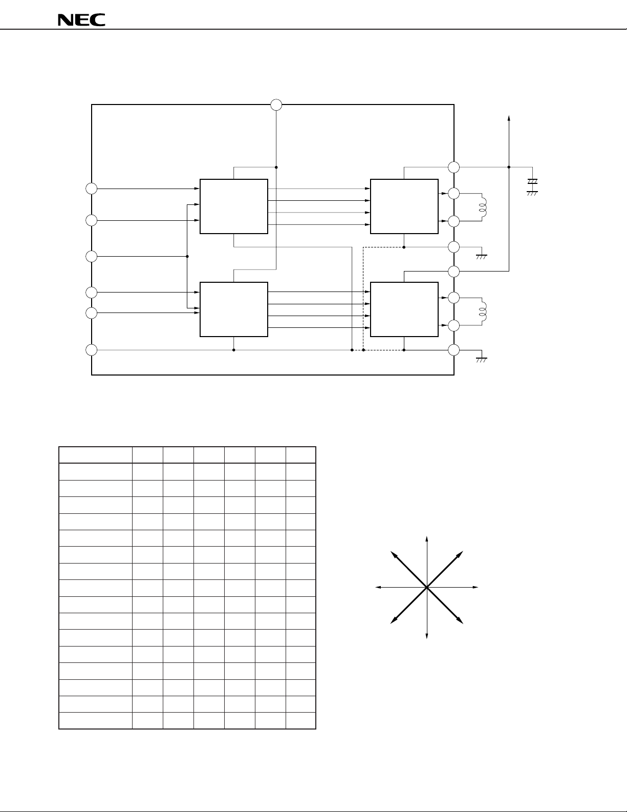
BLOCK DIAGRAM
6IN
1
8IN
2
11SEL
7IN
3
10IN
4
CONTROL
CIRCUIT 1
CONTROL
CIRCUIT 2
µ
PD16814
V
DD
5
V
M
V
M1
“H”
BRIDGE 1
“H”
BRIDGE 2
1
2
15
3
12
4
13
1A
1B
PGND
M2
V
2A
2B
1
+
9DGND 14
FUNCTION TABLE
• In Stop mode (SEL = High)
Excitation Direction
—— LLLLSS
H2R LLLHSR
H2FLLHLSF
—— L L H H S S
H1RLHLLRS
<3> L H L H R R
<2> L H H L R F
H1R LHHHRS
H1F HLLLFS
<4> H L L H F R
<1> HLHLFF
H1FHLHHFS
—— H H L L S S
H2RHHLHSR
H2F HHHLSF
—— HHHHSS
IN1 IN2 IN3 IN4 H1 H2
PGND
2
H
1
F
<4><
2
RH
H
<
><
3
H
1
R
>
1
2
F
>
2
2
Page 3
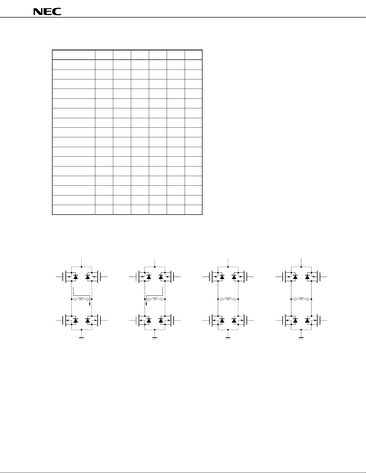
• In Brake mode (SEL = Low)
µ
PD16814
Excitation Direction
IN1 IN2 IN3 IN4 H1 H2
—— LLLLBB
H2R LLLHBR
H2FLLHLBF
—— L L H H B B
H1RLHLLRB
<3> L H L H R R
<2> L H H L R F
H1R LHHHRB
H1F HLLLFB
<4> H L L H F R
<1> HLHLFF
H1FHLHHFB
—— H H L L B B
H2RHHLHBR
H2F HHHLBF
—— HHHHBB
F: Forward R: Reverse S: Stop B: Brake
FORWARD
V
M
ON
AB
OFF
OFF
ON
REVERSE
V
M
OFF
AB
ON
ON
OFF
STOP
V
M
OFF
AB
OFF
OFF
OFF
BRAKE
V
M
OFF
AB
ON
OFF
ON
3
Page 4
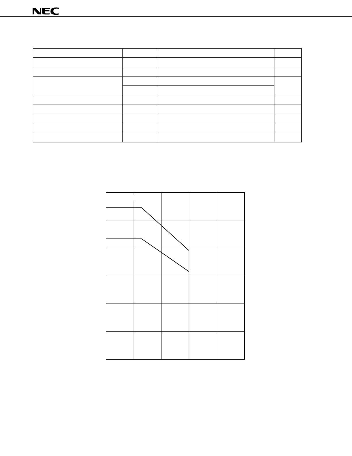
ABSOLUTE MAXIMUM RATINGS (TA = 25 °C)
Parameter Symbol Ratings Unit
Supply voltage (motor block) VM –0.5 to +7 V
Supply voltage (control block) VDD –0.5 to +7 V
Power dissipation Pd1 0.862
Pd2 1.087
Instantaneous H bridge driver current ID (pulse) ±1.0
Input voltage VIN –0.5 to VDD + 0.5 V
Operating temperature TA 0 to 60 °C
Junction temperature Tj MAX. 150 °C
Storage temperature Tstg –55 to +125 °C
Note 1
Note 2
Note 2,3
Notes1. IC alone.
2. When mounted on board (100 × 100 × 1 mm, glass epoxy)
3. t ≤ 5 ms, Duty ≤ 40%
µ
PD16814
W
A
1.2
When mounted
on board
1.0
IC alone
0.8
(W)
d
0.6
0.4
Average power dissipation P
0.2
d
vs. TA Characteristics
P
0
20 40 60 80
A
Ambient temperature T
(°C)
4
Page 5

µ
PD16814
RECOMMENDED OPERATING CONDITIONS (TA = 25 °C)
Parameter Symbol MIN. TYP. MAX. Unit
Supply voltage (motor block) VM 4.0 5.0 6.0 V
Supply voltage (control block) VDD 4.0 5.0 6.0 V
H bridge drive current
Operating temperature TA 060°C
Note
IDR ±415 mA
Note When mounted on board (100 × 100 × 1 mm, glass epoxy)
ELECTRICAL CHARACTERISTICS (Within recommended operating conditions unless otherwise specified)
Parameter Symbol Condition MIN. TYP. MAX. Unit
VM pin current with output transistor OFF IM VM = 6.0 V, VDD = 6.0 V 1.0
VDD pin current IDD 0.1 mA
Control pin high-level input current IIH VIN = VDD 1.0
Control pin low-level input current IIL VIN = 0 V –1.0
Control pin high-level input voltage VIH 3.0
Control pin low-level input voltage VIL –0.3 0.8 V
H bridge circuit ON resistance
RON relative accuracy
H bridge output circuit propagation delay time tPHL VM = 5 V, VDD = 5 V
H bridge output circuit propagation delay time tPLH
H bridge output circuit rise time tTHL VM = 5 V, VDD = 5 V
H bridge output circuit fall time tTLH
Note 1
RON1 VM = 5 V, VDD = 5 V 2.0 4.0 Ω
∆
RON
∆
RON Excitation direction <1>, <3> ±10
Excitation direction <2>, <4>
TA = 25 °C, RM = 20 Ω
TA = 25 °C, RM = 20 Ω
Note 2
Note 3
Note 3
VDD + 0.3
1.8 2.5
0.2 0.65
0.2 0.4
0.1 0.2
µ
A
µ
A
µ
A
V
±5%
µ
s
µ
s
µ
s
µ
s
Notes 1. Sum of ON resistance of top and bottom transistors
2. For the excitation direction, refer to FUNCTION TABLE.
3.
IN1-IN4
tPHL
IM
tTHL
tPLH
tTLH
5
Page 6

TYPICAL CHARACTERISTICS
ON
vs. Tj Characteristics
R
4
µ
PD16814
ON
vs. VDD (= VM) Characteristics
R
4
RON = 20 Ω
3
(Ω)
ON
2
H bridge ON resistance R
1
0
25 50 75 100 125 150
Operating junction temperature Tj (˚C)
t
PHL
vs. TA Characteristics
4
µ
( s)
PHL
3
(Ω)
ON
2
1
H bridge ON resistance R
0
4.0 5.0 6.0
Supply voltage VDD (= VM) (V)
PLH
vs. TA Characteristics
t
0.8
µ
0.7
( s)
PLH
3
2
1
H bridge output curcuit propagation delay time t
0
25 50 75 100 125 150
Operating temperature TA (˚C)
0.6
0.5
0.4
0.3
0.2
0.1
H bridge output curcuit propagation delay time t
0
25 50 75 100 125 150
Operating temperature TA (˚C)
6
Page 7

STEPPING MOTOR EXCITATION TIMING CHART
Inner circumference seek
IN
1
IN
2
IN
3
IN
4
Excitation
direction
H
1
F <1> H2F <2> H1R <3> H2R <4> H1F <1> H2F <2> H1R
Outer circumference seek
IN
1
IN
2
IN
3
IN
4
Excitation
direction
H
1
F <4> H2R <3> H1R <2> H2F <1> H1F <4> H2R <3> H1R
µ
PD16814
• Input signal wave when SEL = LOW (Brake mode)
To set the H bridge in the Brake mode (refer to FUNCTION TABLE), use input signals that set the Brake mode
from IN
2 (IN4).
Example 1 From Forward to Brake
IN1/IN
IN2/IN
3
4
FB
Correct
IN1/IN
IN2/IN
3
4
FB
Incorrect
Example 2 From Reverse to Brake
IN1/IN
IN2/IN
3
4
RB
Correct
IN1/IN
IN2/IN
3
4
RB
Incorrect
Remark This is because noise may be output due to the configuration of the internal circuit.
7
Page 8

µ
NOTES ON PWM DRIVING CONTROL
Keep in mind the following points when executing PWM.
• Be sure to input the signals to control PWM driving from IN
• Because the logic of the PWM driving control inputs (IN2 and IN4) to create the Brake status is inverted depending
on whether the Forward or Reverse mode is used, care must be exercised when PWM driving is controlled at
a duty factor other than 50%.
Example 1 PWM driving in Forward mode
IN1/IN
3
IN2/IN
4
2 and IN4.
IN1/IN
3
IN2/IN
4
PD16814
FBFBFBFBFBF
Correct
FBFBFBFBFBF
Incorrect
Example 2 PWM driving in Reverse mode
IN1/IN
IN2/IN
3
4
RBRBRBRBRBR
Correct
IN1/IN
IN2/IN
3
4
RBRBRBRBRBR
Incorrect
Remark This is because noise may be output due to the configuration of the internal circuit.
8
Page 9

PACKAGE DIMENSION
16 PIN PLASTIC SOP (300 mil)
18
µ
PD16814
916
detail of lead end
P
A
G
F
E
C
D
NOTE
Each lead centerline is located within 0.12 mm (0.005 inch) of
its true position (T.P.) at maximum material condition.
N
M
M
B
H
I
J
K
L
ITEM MILLIMETERS INCHES
A
10.46 MAX.
B
0.78 MAX.
C
1.27 (T.P.)
D 0.40 0.016
E
F
G
H
I
J
K 0.20
L 0.6±0.2 0.024
M
N
P3° 3°
+0.10
–0.05
0.1±0.1
1.8 MAX.
1.55
7.7±0.3
5.6
1.1
+0.10
–0.05
0.12
0.10
+7°
–3°
0.412 MAX.
0.031 MAX.
0.050 (T.P.)
+0.004
–0.003
0.004±0.004
0.071 MAX.
0.061
0.303±0.012
0.220
0.043
+0.004
0.008
–0.002
+0.008
–0.009
0.005
0.004
+7°
–3°
P16GM-50-300B-4
9
Page 10

µ
RECOMMENDED SOLDERING CONDITIONS
It is recommended to solder this product under the conditions shown below.
For soldering methods and conditions other than those listed below, consult NEC.
For details of the recommended soldering conditions, refer to Information Document “Semiconductor Device
Mounting Technology Manual” (C10535E).
Surface Mount Type
Soldering Method Soldering Condition
Infrared reflow Package peak temperature: 235 °C, Time: 30 seconds MAX. (210 °C MIN.) IR35-00-2
Number of times: 2 MAX.
<Precautions>
(1) Start the second reflow after the device temperature rise due to the first
reflow has dropped to room temperature.
(2) Do not clean flux with water after the first reflow.
VPS Package peak temperature: 215 °C, Time: 40 seconds MAX. (200 °C MIN.) VP15-00-2
Number of times: 2 MAX.
<Precautions>
(1) Start the second reflow after the device temperature rise due to the first
reflow has dropped to room temperature.
(2) Do not clean flux with water after the first reflow.
Wave soldering Soldering bath temperature: 260 °C MAX., Time: 10 seconds MAX., WS60-00-1
Number of times: 1
Preheating temperature: 120 °C MAX. (package surface temperature)
Partial heating Pin temperature: 300 °C MAX., Time: 3 seconds MAX. (per side of device) –
Symbol of Recommended
Soldering
PD16814
Caution Do not use two or more soldering methods in combination (except partial heating).
10
Page 11

µ
NOTES FOR CMOS DEVICES
1 PRECAUTION AGAINST ESD FOR SEMICONDUCTORS
Note: Strong electric field, when exposed to a MOS device, can cause destruction
of the gate oxide and ultimately degrade the device operation. Steps must
be taken to stop generation of static electricity as much as possible, and
quickly dissipate it once, when it has occurred. Environmental control must
be adequate. When it is dry, humidifier should be used. It is recommended
to avoid using insulators that easily build static electricity. Semiconductor
devices must be stored and transported in an anti-static container, static
shielding bag or conductive material. All test and measurement tools
including work bench and floor should be grounded. The operator should
be grounded using wrist strap. Semiconductor devices must not be touched
with bare hands. Similar precautions need to be taken for PW boards with
semiconductor devices on it.
PD16814
2 HANDLING OF UNUSED INPUT PINS FOR CMOS
Note: No connection for CMOS device inputs can be cause of malfunction. If no
connection is provided to the input pins, it is possible that an internal input
level may be generated due to noise, etc., hence causing malfunction. CMOS
device behave differently than Bipolar or NMOS devices. Input levels of
CMOS devices must be fixed high or low by using a pull-up or pull-down
circuitry. Each unused pin should be connected to VDD or GND with a
resistor, if it is considered to have a possibility of being an output pin. All
handling related to the unused pins must be judged device by device and
related specifications governing the devices.
3 STATUS BEFORE INITIALIZATION OF MOS DEVICES
Note: Power-on does not necessarily define initial status of MOS device. Produc-
tion process of MOS does not define the initial operation status of the device.
Immediately after the power source is turned ON, the devices with reset
function have not yet been initialized. Hence, power-on does not guarantee
out-pin levels, I/O settings or contents of registers. Device is not initialized
until the reset signal is received. Reset operation must be executed immediately after power-on for devices having reset function.
11
Page 12

µ
PD16814
No part of this document may be copied or reproduced in any form or by any means without the prior written
consent of NEC Corporation. NEC Corporation assumes no responsibility for any errors which may appear in
this document.
NEC Corporation does not assume any liability for infringement of patents, copyrights or other intellectual property
rights of third parties by or arising from use of a device described herein or any other liability arising from use
of such device. No license, either express, implied or otherwise, is granted under any patents, copyrights or other
intellectual property rights of NEC Corporation or others.
While NEC Corporation has been making continuous effort to enhance the reliability of its semiconductor devices,
the possibility of defects cannot be eliminated entirely. To minimize risks of damage or injury to persons or
property arising from a defect in an NEC semiconductor device, customers must incorporate sufficient safety
measures in its design, such as redundancy, fire-containment, and anti-failure features.
NEC devices are classified into the following three quality grades:
"Standard", "Special", and "Specific". The Specific quality grade applies only to devices developed based on a
customer designated "quality assurance program" for a specific application. The recommended applications of
a device depend on its quality grade, as indicated below. Customers must check the quality grade of each device
before using it in a particular application.
Standard: Computers, office equipment, communications equipment, test and measurement equipment,
audio and visual equipment, home electronic appliances, machine tools, personal electronic
equipment and industrial robots
Special: Transportation equipment (automobiles, trains, ships, etc.), traffic control systems, anti-disaster
systems, anti-crime systems, safety equipment and medical equipment (not specifically designed
for life support)
Specific: Aircrafts, aerospace equipment, submersible repeaters, nuclear reactor control systems, life
support systems or medical equipment for life support, etc.
The quality grade of NEC devices is "Standard" unless otherwise specified in NEC's Data Sheets or Data Books.
If customers intend to use NEC devices for applications other than those specified for Standard quality grade,
they should contact an NEC sales representative in advance.
Anti-radioactive design is not implemented in this product.
M4 96.5
2
 Loading...