

Page 1
DATA SHEET
MOS INTEGRATED CIRCUIT
µ
PD16808
MONOLITHIC DUAL H BRIDGE DRIVER CIRCUIT
DESCRIPTION
The µPD16808 is a monolithic dual H bridge driver circuit which employing N-channel power MOS FETs for its driver
stage. By using the power MOS FETs for the output stage, saturation voltage and power consumption are substantially
improved as compared with conventional driver circuits that use bipolar transistors.
Because the dual H bridge driver circuits at the output stage are independent of each other, this IC is ideal as the driver
circuit for a 1- to 2-phase excitation bipolar driving stepping motor for the head actuator of an FDD.
FEATURES
• Low ON resistance (sum of ON resistors of top and bottom FETS)
ON1 = 1.0 Ω TYP. (VM = 5.0 V)
R
RON2 = 1.5 Ω TYP. (VM = 12.0 V)
• Low current consumption: IDD = 0.4 mA TYP.
• Four input modes independently controlling dual H bridge drivers (with 1- to 2-phase excitation selected)
• Motor voltage 12 V/5 V compatible
• Compact surface mount package: 20-pin plastic SOP (300 mil)
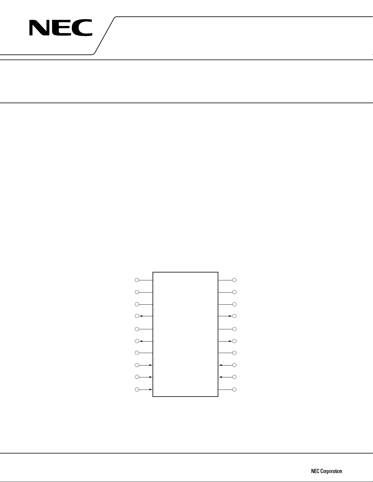
PIN CONFIGURATION (Top View)
C1H
C2L
V
M1
1A
1
PGND
2A
V
DD
IN
1
IN
2
IN
3
1
2
3
4
5
6
7
8
9
10
20
19
18
17
16
15
14
13
12
11
C1L
C2H
V
G
1B
PGND
2B
V
M2
SEL
4
IN
DGND
2
Document No. S12720EJ2V0DS00 (2nd edition)
Date Published September 1997 N
Printed in Japan
©
1997
Page 2
ORDERING INFORMATION
Part Number Package
µ
PD16808GS 20-pin plastic SOP (300 mil)
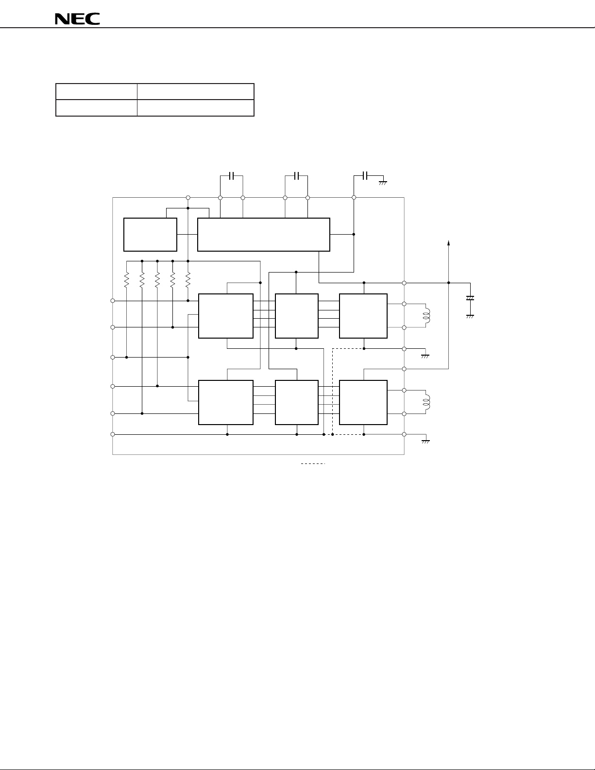
BLOCK DIAGRAM
0.01 F
µ
0.01 F
µ
0.01 F
µ
µ
PD16808
IN
IN
SEL
IN
IN
DGND
C1L C2LC1H C2H
V
DD
OSC
CIRCUIT
1
2
3
4
CHARGE PUMP
CONTROL
CIRCUIT 1
CONTROL
CIRCUIT 2
LEVEL
SHIFT 1
LEVEL
SHIFT 2
V
G
2 × V
“H”
BRIDGE 1
“H”
BRIDGE 2
DD
+ V
M
V
M1
1A
V
M
+
1B
PGND
1
V
M2
2A
2B
2
PGND
Connected in diffusion layer
2
Page 3
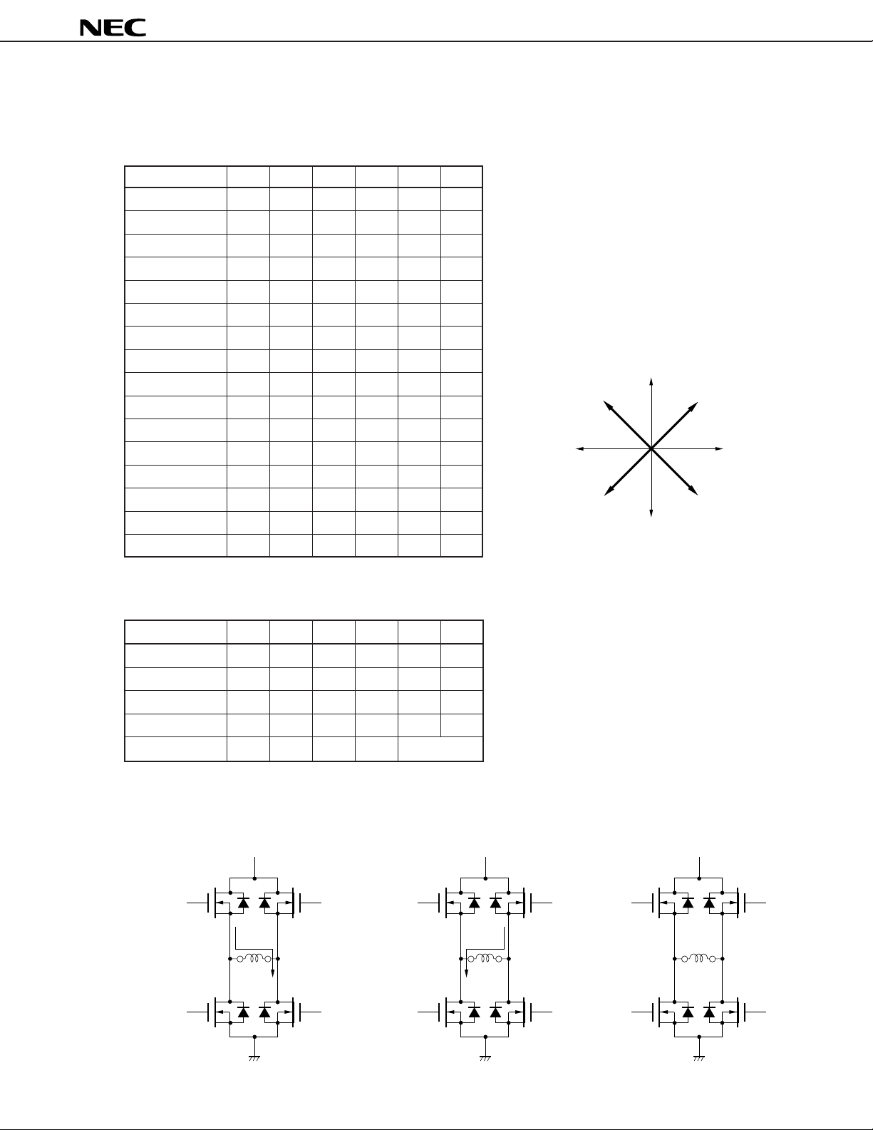
FUNCTION TABLE
• With 1- to 2-phase excitation selected (SEL = High)
µ
PD16808
Excitation Direction
—— LLLLSS
H2R LLLHSR
H2FLLHLSF
—— L L H H S S
H1RLHLLRS
<3> L H L H R R
<2> L H H L R F
H1R LHHHRS
H1F HLLLFS
<4> H L L H F R
<1> HLHLFF
H1FHLHHFS
—— H H L L S S
H2RHHLHSR
H2F HHHLSF
—— HHHHSS
IN1 IN2 IN3 IN4 H1 H2
H2R
<4>
H
1
F
<1>
H
2
F
<2><3>
1
R
H
• With 2-phase excitation selected (SEL = Low)
Excitation Direction
<1> H H × HFF
<2> L H × HRF
<3> L L × HRR
<4> H L × HFR
– ×××L Stop
F: Forward R: Reverse S: Stop ×: Don’t care
IN1 IN3 IN4 IN2 H1 H2
For the excitation waveform timing chart, refer to APPLICATION CIRCUIT EXAMPLE.
FORWARD
M
V
ON
AB
OFF
OFF
ON
OFF
REVERSE
M
V
AB
ON
ON
OFF
STOP
M
V
OFF
AB
OFF
OFF
OFF
3
Page 4
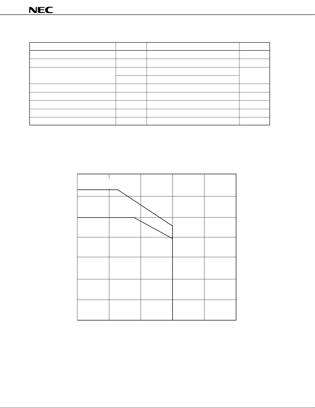
ABSOLUTE MAXIMUM RATINGS (TA = 25 °C)
Parameter Symbol Rating Unit
Supply voltage (motor block) VM –0.5 to +15 V
Supply voltage (control block) VDD –0.5 to +7 V
Power dissipation Pd1 1.0
Pd2 1.25
Instantaneous H bridge driver current ID (pulse) ±1.0
Input voltage VIN –0.5 to VDD + 0.5 V
Operating temperature range TA 0 to 60 °C
Operation junction temperature TjMAX. 150 °C
Storage temperature range Tstg –55 to +125 °C
Note 1
Note 2
Note 2, 3
Notes 1. IC only
2. When mounted on a printed circuit board (100 × 100 × 1 mm, glass epoxy)
3. t ≤ 5 ms, Duty ≤ 40 %
µ
PD16808
W
A
1.4
When mounted
on printed circuid boad
1.2
IC only
1.0
(W)
d
0.8
0.6
Average power dissipation P
0.4
0.2
P
d
– TA Characteristics
0 20 40 60 80 100
Ambient temperature TA (˚C)
4
Page 5

µ
PD16808
RECOMMENDED OPERATING CONDITIONS
Parameter Symbol MIN. TYP. MAX. Unit
Supply voltage (motor block) VM 4.0 5.0 13.2 V
Supply voltage (control block) VDD 4.0 5.0 6.0 V
H bridge driver current
VM = 5.0 V 2-phase excitation
Charge pump capacitance C1 to C3 520nF
Operating temperature TA 060°C
Note
1-/2-phase excitation IDR ± 600 mA
±450
Note When mounted on a printed circuit board (100 × 100 × 1 mm, glass epoxy)
ELECTRICAL SPECIFICATIONS (Within recommended operating conditions unless otherwise specified)
Parameter Symbol Conditions MIN. TYP. MAX. Unit
OFF VM pin current IM VM = 6.0 V, VDD = 6.0 V
VM = 13.2 V, VDD = 6.0 V
VDD pin current IDD Note 2 0.4 1.0 mA
Control pin high-level input IIH TA = 25 °C, VIN = VDD 1.0
current 0 ≤ TA ≤ 60 °C, VIN = VDD 2.0
Control pin low-level input IIL TA = 25 °C, VIN = 0 V –0.18 mA
current 0 ≤ TA ≤ 60 °C, VIN = 0 V –0.25
Control pin input pull-up RIN TA = 25 °C 355065kΩ
resistance 0 ≤ TA ≤ 60 °C2575
Control pin high-level input voltage
Control pin low-level input voltage VIL –0.3 0.8 V
H bridge circuit ON RON1 VDD = 5 V, VM = 5 V 1.0 2.0 Ω
resistance
RON relative accuracy
Charge pump circuit (VG) turn-ON time
H bridge circuit turn-ON time TONH C1 = C2 = C3 = 10 nF 5
H bridge circuit turn-OFF time TOFFH RM = 20 Ω 5
Note 3
VIH 3.0 VDD + 0.3 V
RON2 VDD = 5 V, VM = 12 V 1.5 3.0 Ω
∆
RON1 Excitation direction <2>, <4>
∆
RON2 Excitation direction <1>, <3> ±10
TONG VDD = 5 V, VM = 5 V 0.2 1.0 ms
Note 1
Note 1
Note 4
1.0
1.0 mA
±5%
µ
A
µ
A
µ
s
µ
s
Notes 1. Control pins (IN1, IN2, IN3, IN4): low
2. Control pins (IN
1, IN2, IN3, IN4): high
3. Sum of ON resistances of top and bottom transistors
4. For the excitation direction, refer to FUNCTION TABLE.
5
Page 6

CHARACTERISTIC CURVES
µ
PD16808
RON vs. VDD (= VM) Characteristics
3
(Ω) H bridge ON resistance R
ON
2
1
H bridge ON resistance R
0
4.0 10 11 12 13 145.0 6.0
Supply voltage VDD (= VM) (V)
R
ON
vs. Tj Characteristics
3
RM = 20
Ω
VDD = VM =5.0 V
R
M
= 20 Ω
RON vs. VM Characteristics
3
(Ω)
ON
2
1
H bridge ON resistance R
0
Motor voltage V
M
(V)
RM = 100
VDD = 4.5 V
V
DD
= 5.0 V
DD
= 5.5 V
V
Ω
(Ω)
ON
2
1
0
Operation junction temperature T
50 100 150
j
(˚C)
6
Page 7

Step input
µ
PC2100AGF Stepping Motor Excitation Timing Chart
APPLICATION CIRCUIT EXAMPLE
• Connection with 1-chip FDD LSI
Direction
Internal circumference seek
External circumference seek
PH11
PH21
PH31
µ
PC2100AGF (With 1- to 2-phase excitation selected)
PH41
0.01 F
0.01 F
C2L
LEVEL
SHIFT 1
LEVEL
SHIFT 2
µ
C2H
PH11
PH21
PH31
PH41
IN
IN
V
SEL
IN
IN
0.01 F
µ
C1L
V
DD
OSC
CIRCUIT
1
2
DD
3
4
CONTROL
CIRCUIT 1
CONTROL
CIRCUIT 2
C1H
CHARGE PUMP
DGND
µ
PC2100AGF
7
Connected in diffusion layer
µ
V
G
2 × V
DD
“H”
BRIDGE 1
“H”
BRIDGE 2
+
V
M
V
1A
V
M
M1
+
1B
1
PGND
V
M2
2A
2B
PGND
2
µ
PD16808
Page 8

8
• Connection with 1-chip FDD LSI
The application circuits and their parameters are for reference only and are not intended for use in actual design-ins.
µ
PC2100AGF Stepping Motor Excitation Timing Chart
Step input
SPF0
PH11
PH21
Direction
PH11
PH21
DGND
IN1
IN2
SEL
IN3
IN4
Internal circumference seek
0.01 F
µ
C1L
V
DD
OSC
CIRCUIT
CHARGE PUMP
CONTROL
CIRCUIT 1
CONTROL
CIRCUIT 2
C1H
C2L
LEVEL
SHIFT 1
LEVEL
SHIFT 2
External circumference seek
0.01 F
µ
C2H
0.01 F
V
G
2 × V
“H”
BRIDGE 1
“H”
BRIDGE 2
µ
PC2100AGF (With 2-phase exication selected)
µ
DD
+
V
M
V
1A
V
M
M1
+
1B
1
PGND
V
M2
2A
2B
PGND
2
PC2100AGF
µ
Connected in diffusion layer
µ
PD16808
Page 9

20 PIN PLASTIC SOP (300 mil)
110
µ
PD16808
1120
detail of lead end
P
A
G
F
E
C
D
NOTE
Each lead centerline is located within 0.12 mm (0.005 inch) of
its true position (T.P.) at maximum material condition.
N
M
M
H
I
J
K
B
L
ITEM MILLIMETERS INCHES
A
13.00 MAX.
B
0.78 MAX.
C
1.27 (T.P.)
D 0.40 0.016
E
F
G
H
I
J
K 0.20
L 0.6±0.2 0.024
M
N
P3° 3°
+0.10
–0.05
0.1±0.1
1.8 MAX.
1.55
7.7±0.3
5.6
1.1
+0.10
–0.05
0.12
0.10
+7°
–3°
0.512 MAX.
0.031 MAX.
0.050 (T.P.)
+0.004
–0.003
0.004±0.004
0.071 MAX.
0.061
0.303±0.012
0.220
0.043
+0.004
0.008
–0.002
+0.008
–0.009
0.005
0.004
+7°
–3°
P20GM-50-300B, C-4
9
Page 10

µ
RECOMMENDED SOLDERING CONDITIONS
It is recommended to solder this product under the conditions described below.
For soldering methods and conditions other than those listed below, consult NEC.
Surface mount type
For the details of the recommended soldering conditions of this type, refer to Semiconductor Device Mounting
Technology Manual (C10535E).
PD16808
Soldering Method Soldering Conditions
Infrared reflow
VPS
Wave soldering Solder bath temperature: 260 °C MAX., Time: 10 seconds MAX., WS60-00
Partial heating
Peak package temperature: 230 °C, Time: 30 seconds MAX. (210 °C MIN.),
Number of times: 1, Number of days: None
Peak package temperature: 215 °C, Time: 40 seconds MAX. (200 °C MIN.),
Number of times: 1, Number of days: None
Number of times: 1, Number of days: None
Pin temperature: 300 °C MAX., Time: 10 seconds MAX., –
Number of days: None
Note
Note
Note
Note
Symbol of Recommended
Soldering
IR30-00
VP15-00
Note The number of storage days at 25 °C, 65 % RH after the dry pack has been opened
Caution Do not use two or more soldering methods in combination (except partial heating).
10
Page 11

[MEMO]
µ
PD16808
11
Page 12

µ
PD16808
[MEMO]
No part of this document may be copied or reproduced in any form or by any means without the prior written
consent of NEC Corporation. NEC Corporation assumes no responsibility for any errors which may appear in
this document.
NEC Corporation does not assume any liability for infringement of patents, copyrights or other intellectual property
rights of third parties by or arising from use of a device described herein or any other liability arising from use
of such device. No license, either express, implied or otherwise, is granted under any patents, copyrights or other
intellectual property rights of NEC Corporation or others.
While NEC Corporation has been making continuous effort to enhance the reliability of its semiconductor devices,
the possibility of defects cannot be eliminated entirely. To minimize risks of damage or injury to persons or
property arising from a defect in an NEC semiconductor device, customers must incorporate sufficient safety
measures in its design, such as redundancy, fire-containment, and anti-failure features.
NEC devices are classified into the following three quality grades:
"Standard", "Special", and "Specific". The Specific quality grade applies only to devices developed based on a
customer designated "quality assurance program" for a specific application. The recommended applications of
a device depend on its quality grade, as indicated below. Customers must check the quality grade of each device
before using it in a particular application.
Standard: Computers, office equipment, communications equipment, test and measurement equipment,
audio and visual equipment, home electronic appliances, machine tools, personal electronic
equipment and industrial robots
Special: Transportation equipment (automobiles, trains, ships, etc.), traffic control systems, anti-disaster
systems, anti-crime systems, safety equipment and medical equipment (not specifically designed
for life support)
Specific: Aircrafts, aerospace equipment, submersible repeaters, nuclear reactor control systems, life
support systems or medical equipment for life support, etc.
The quality grade of NEC devices is "Standard" unless otherwise specified in NEC's Data Sheets or Data Books.
If customers intend to use NEC devices for applications other than those specified for Standard quality grade,
they should contact an NEC sales representative in advance.
Anti-radioactive design is not implemented in this product.
M4 96.5
2
 Loading...