

Page 1

DATA SHEET
MOS INTEGRATED CIRCUIT
µµµµ
PD16520
VERTICAL DRIVER FOR CCD SENSORS
The µPD16520 is a vertical driver for CCD image sensors that has a level conversion circuit and a 3-level output
function. Since it incorporates a CCD vertical register driver equivalent to the µPD16510 (10 channels, consisting of
six 3-level channels and four 2-level channels) and a VOD shutter driver (1 channel), it is ideal as a vertical driver for
multiple-electrode high-pixel CCD transfer type area image sensors employed in digital still cameras.
The µPD16520 uses a CMOS process to achieve optimum transmission delay characteristics for vertical driving of
CCD image sensors, as well as output on-state resistance characteristics. The µPD16520 also supports low-voltage
logic (logic supply voltage: 2.0 to 5.5 V).
FEATURES
CCD vertical register driver: 10 channels (3-level: 6 channels, 2-level: 4 channels)
•
VOD shutter driver: 1 channel
•
High withstand voltage: 33 V Max.
•
Low-output on-state resistance: 30 Ω TYP.
•
Low-voltage input supported (Logic supply voltage: 2.0 to 5.5 V)
•
Latch-up free
•
Same drive capacity as
•
Small package: 38-pin plastic shrink SOP (300 mil)
•
APPLICATIONS
Digital still cameras, digital video cameras, etc.
ORDERING INFORMATION
Part Number Package
PD16520GS-BGG 38-pin plastic shrink SOP (300 mil)
µ
PD16510
µ
The information in this document is subject to change without notice. Before using this document, please
confirm that this is the latest version.
Not all devices/types available in every country. Please check with local NEC representative for
availability and additional information.
Document No. S14201EJ1V0DS00 (1st edition)
Date Published May 1999 N CP(K)
Printed in Japan
©
1999
Page 2
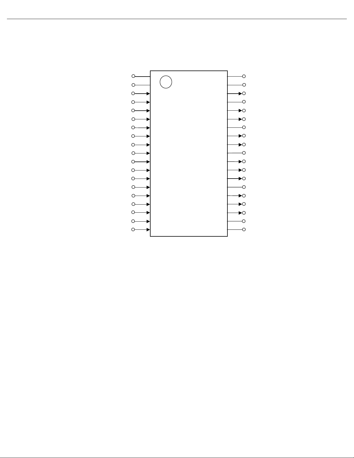
PIN CONFIGURATION (TOP VIEW)
38-pin plastic shrink SOP (300 mil)
•
PD16520GS-BGG
µ
µµµµ
PD16520
GND
Vcc
TI1
TI2
TI3
TI4
TI5
TI6
PG1
PG2
PG3
PG4
PG5
PG6
BI1
BI2
BI3
BI4
SUBI
1
2
3
4
5
6
7
8
9
10
11
12
13
14
15
16
17
18
19
38
37
36
35
34
33
32
31
30
29
28
27
26
25
24
23
22
21
20
V
SS
VDD1
TO1
VDD2a
TO2
TO3
VDD2a
TO4
TO5
VDD2a
TO6
BO1
BO2
VDD2b
BO3
BO4
SUBO
Vsb
Vss
PIN NAMES
BI1 to BI4: 2 Level Driver Input TO1 to TO6: 3 Level Pulse Output
BO1 to BO4: 2 Level Pulse Output VDD1: Power Supply (VH)
GND: Ground VDD2a: Power Supply (VMa)
PG1 to PG6: 3 Level Driver Input VDD2b: Power Supply (VMb)
SUBI: VOD Shutter Drive Pulse Input VCC: Power Supply (Logic)
SUBO: VOD Shutter Drive Pulse Output Vsb: Power Supply (VHH)
TI1 to TI6: 3 Level Driver Input VSS: Power Supply (VL)
2
Data Sheet S14201EJ1V0DS00
Page 3
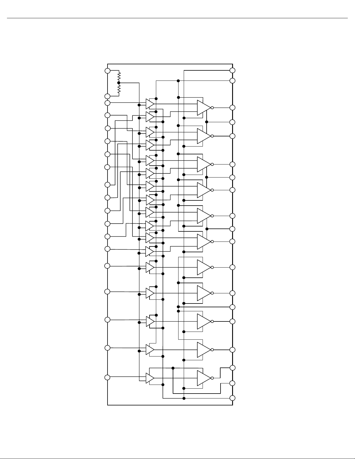
BLOCK DIAGRAM
GND
Vcc
TI1
TI2
TI3
TI4
TI5
TI6
PG1
PG2
PG3
PG4
PG5
PG6
µµµµ
PD16520
Vss
1
2
3
4
5
6
7
8
9
10
11
12
13
14
+
−
+
−
+
−
+
−
+
−
+
−
+
−
+
−
+
−
+
−
+
−
+
−
3 level
3 level
3 level
3 level
3 level
3 level
38
37
36
35
34
33
32
31
30
29
28
VDD1
TO1
VDD2a
TO2
TO3
VDD2a
TO4
TO5
VDD2a
TO6
BI1
BI2
BI3
BI4
SUBI
1
16
17
18
19
+
−
+
−
+
−
+
−
+
−
2 level
2 level
2 level
2 level
2 level
27
26
25
24
23
22
21
20
BO1
BO2
VDD2b
BO3
BO4
SUBO
Vsb
Vss
Data Sheet S14201EJ1V0DS00
3
Page 4

1. PIN FUNCTIONS
Pin No. Pin Name I/O Function
1GND
2V
3TI1 I
4TI2 I
5TI3 I
6TI4 I
7TI5 I
8TI6 I
9PG1 I
10 PG2 I
11 PG3 I
12 PG4 I
13 PG5 I
14 PG6 I
15 BI1 I
16 BI2 I
17 BI3 I
18 BI4 I
19 SUBI I VOD shutter drive pulse input
20 V
21 Vsb
22 SUBO O VOD shutter drive pulse out put
23 BO4 O
24 BO3 O
25 VDD2b
26 BO2 O
27 BO1 O
28 TO6 O 3-level pulse output
29 VDD2a
30 TO5 O
31 TO4 O
32 VDD2a
33 TO3 O
34 TO2 O
35 VDD2a
36 TO1 O 3-level pulse output
37 VDD1
38 V
µµµµ
PD16520
Ground
−
CC
SS
SS
Logic power supply
−
3-level driver input (for charge t ransfer) (See Function
Tables.)
3-level driver input (for charge read) (S ee Function
Tables.)
2-level driver input (for charge t ransfer) (See Function
Tables.)
L
V
power supply
−
VHH power supply (for SUB drive)
−
2-level pulse output
VMb power supply (for 2-level driver)
−
2-level pulse output
VMa power supply (for 3-level driver)
−
3-level pulse output
VMa power supply (for 3-level driver)
−
3-level pulse output
VMa power supply (for 3-level driver)
−
VH power supply
−
L
V
power supply
−
4
Data Sheet S14201EJ1V0DS00
Page 5
µµµµ
PD16520
Function Tables
L
= VSS, VMa = VDD2a, VMb = VDD2b, VH = VDD1, VHH = Vsb
V
Pins TO1 to TO6
Input Output
Pin Name TI1 TI2 TI3 TI4 TI5 TI6 PG1 PG2 PG3 PG4 PG5 PG6 TO1 TO2 TO3 TO4 TO5 TO6
Pin No. 34567891011121314363433313028
LLV
LHV
HL V
HH V
H
Ma
L
L
Pins BO1 to BO4
Input Output
Pin Name BI1 BI2 BI3 BI4 BO1 BO2 BO3 BO4
Pin No. 1516171827262423
LV
HV
Mb
L
Pin SUBO
Input Output
Pin Name SUBI SUBO
Pin No. 19 22
LV
HV
HH
L
Data Sheet S14201EJ1V0DS00
5
Page 6

2. ELECTRICAL SPECIFICATIONS
µµµµ
PD16520
Absolute Maximum Ratings (TA = 25
C, GND = 0 V)
°°°°
Parameter Symbol Conditions Ratings Unit
Supply voltage
Input pin voltage V
Operating ambient temperature T
Storage temperature T
Allowable dissipation P
V
CC
V
VDD1 V
VDD2 V
Vsb V
I
A
stg
d
0.0 to −10 V
V
V
SS
SS
SS
SS
−
−
−
−
SS
0.3 to V
0.3 to V
0.3 to V
0.3 to V
−
−
0.3 to V
25 to +85
−
40 to +125
SS
+ 20.0 V
SS
+ 33.0 V
SS
+ 33.0 V
SS
+ 33.0 V
CC
+ 0.3 V
500 mW
C
°
C
°
SS
Caution Product quality may suffer if the absolute maximum rating is exceeded even momentarily for any
parameter. That is, the absolute maximum ratings are rated values at which the product is on the
verge of suffering physical damage, and therefore the product must be used under conditions that
ensure that the absolute maximum ratings are not exceeded.
Recommended Operating Range (T
Parameter Symbol Conditions MIN. TYP. MAX. Unit
Supply voltage
Input voltage, high V
Input voltage, low V
Operating ambient temperature T
SS
Set VDD1 and V
Note
to values that satisfy VDD1-VSS rating.
A
CC
V
VDD1
VDD1-V
VDD2a
VDD2b
SS
V
Vsb-V
IH
IL
A
= 25
C, GND = 0 V)
°°°°
SS
SS
Note
Note
Note
2.0 5.5 V
10.5 15.0 21.0 V
16.5 31.0 V
1.0 +4.0 V
−
1.0 +4.0 V
−
−
10.0
6.0 V
−
31.0 V
CC
0.8V
00.3V
20 +70
−
CC
V
V
CC
V
°
C
6
Data Sheet S14201EJ1V0DS00
Page 7

µµµµ
PD16520
Electrical Specifications
(
Unless otherwise specified, VDD1 = +15 V, VDD2a = 0 V, VDD2b = +1.0 V, Vsb = +21.5 V, VCC = +2.5 V, VSS =
7.0 V, TA = 25
−−−−
Output voltage, high V
Output voltage, low V
Output voltage, sub-high V
Output voltage, sub-low V
Output on-state resistance
Transmission delay ti m e 1 TD1 200 ns
Transmission delay ti m e 2 TD2 200 ns
Transmission delay ti m e 3 TD3
Rise/fall time 1 TP1 500 ns
Rise/fall time 2 TP2 500 ns
Rise/fall time 3 TP3
C, GND = 0 V)
°°°°
Parameter Symbol Conditions MIN. TYP. MAX. Unit
H
Ma
V
Mb
V
L
subH
subL
L
R
M
R
H
R
sub
R
IO = −20 µA VDD1 − 0 .1 VDD1 V
IO = −20 µA VDD2a − 0 . 1 VDD2a VOutput voltage, middle
IO = 20 µA VDD2b VDD2b + 0.1 V
IO = 20 µAVSSV
IO = −20 µAVsb
0.1 Vsb V
−
IO = 20 µAVSSV
SS
+ 0.1 V
SS
+ 0.1 V
IO = 10 mA 20 30
IO = ±10 mA 30 45
IO = −10 mA
30 40
30 40
Ω
Ω
Ω
Ω
No load
See
Figure 2-2 Timing Charts
.
200 ns
See
Figure 2-1 Output Load
Equivalence Circuit
See
Figure 2-2 Timing Charts
.
.
200 ns
Data Sheet S14201EJ1V0DS00
7
Page 8

Figure 2-1. Output Load Equivalence Circuit
(a) Between output pins (b) Between output pin and GND
µµµµ
PD16520
BO2
BO3
BO1
R8
R9
BO2'
BO1'
R7
BO3'
BO4
R10
TO6'
TO6
BO4'
R6
TO5'
R1
TO1
TO1'
R5
TO5
TO4'
R2
TO2'
TO3'
R4
R3
TO2
TO4
TO3
BO2
BO3
BO1
R8
R9
BO3'
BO2'
R7
BO4
R10
BO4'
C8
BO1'
TO6
C10
C9
C7
SUB0
R6
C6
TO6'
TO1'
C1
RGND
R1
C5
C2
TO5'
C11
TO1
TO2'
C3
C4
R5
TO5
TO4'
R2
TO3'
R4
R3
TO2
TO3
TO4
Output Load Capacitance Symbol
TO1' TO2' TO3' TO4' TO5' TO6' BO1' BO2' BO3' BO4' GND
TO1'
−
TO2' C_33
TO3' C_33 C_33
TO4' C_33 C_33 C_33
TO5' C_33 C_33 C_33 C_33
TO6' C_33 C_33 C_33 C_33 C_33
BO1' C_32 C_23 C_32 C_23 C_32 C_23
BO2' C_23 C_32 C_23 C_32 C_23 C_32 C_22
BO3' C_32 C_23 C_32 C_23 C_32 C_23 C_22 C_22
BO4' C_23 C_32 C_23 C_32 C_23 C_32 C_22 C_22 C_22
SUBO
−−−−−−−−−−
8
C_33 C_33 C_33 C_33 C_33 C_32 C_23 C_32 C_23 C1
−
C_33 C_33 C_33 C_33 C_23 C_32 C_23 C_32 C2
−
C_33 C_33 C_33 C_32 C_23 C_32 C_23 C3
−
C_33 C_33 C_23 C_32 C_23 C_32 C4
−
C_33 C_32 C_23 C_32 C_23 C5
−
C_23 C_32 C_23 C_32 C6
−
C_22 C_22 C_22 C7
−
C_22 C_22 C8
−
Data Sheet S14201EJ1V0DS00
C_22 C9
−
C10
C11
Page 9

Output Load Equivalence Circuit Constants
Parameter Symbol Constant
Vertical register serial resistor R1 to R10 0
Vertical register ground resi stor RGND 0
Ω
Ω
Capacitance 1 between vertic al regi ster clocks (3 level-3 level) C_33 0 pF
Capacitance 2 between vertic al regi ster clocks (2 level-2 level) C_22 0 pF
Capacitance 3 between vertic al regi ster clocks (3 level-2 level) C_32 1000 pF
Capacitance 4 between vertic al regi ster clocks (2 level-3 level) C_23 500 pF
Vertical register ground capacitance 1 (3 level) C1 to C6 3000 pF
Vertical register ground capacitance 2 (2 level) C7 to C10 1500 pF
Substrate ground capacitanc e C11 1600 pF
Figure 2-2. Timing Charts
BI1 to BI4
TI1 to TI6
TD1 TD1
µµµµ
PD16520
BO1 to BO4
TO1 to TO6
PG1 to PG6
TO1 to TO6
SUBI
TP1
TD2 TD2
TP2
TP1
TP2
Mb
V
Ma
V
L
V
H
V
Ma
V
SUBO
TD3 TD3
TP3
Data Sheet S14201EJ1V0DS00
TP3
HH
V
L
V
9
Page 10

3. CAUTIONS
3.1 Power ON/OFF Sequence
µµµµ
PD16520
In the
BI4, SUBI) → VCC, so that in the case of voltage conditions: VDD2 > VDD1, input pin voltage (TI1 to TI6, PG1 to
PG6, BI1 to BI4, SUBI) > VCC, an abnormal current flows. Therefore, when turning the power ON/OFF, make sure
that the following voltage conditions are satisfied: VDD2 ≤ VDD1, input pin voltage (TI1 to TI6, PG1 to PG6, BI1 to
BI4, SUBI) ≤ VCC. Also, to minimize the negative potential applied to the SUB pin of the CCD image sensor, following
the power ON/OFF sequence described below.
(1) Power ON
PD16520, a PN junction (diode) exists between VDD2 → VDD1, input pin (TI1 to TI6, PG1 to PG6, BI1 to
µ
<1> Powering ON V
Make sure that input pin voltage (TI1 to TI6, PG1 to PG6, BI1 to BI4, SUBI) ≤ VCC. Also, when Vsb = 2 V,
make sure that VCC reaches the rated voltage.
<2> Powering ON Vsb, VDD1, VDD2a, VDD2b, V
At this time, make SUBI high level (0.8VCC or higher).
CC
SS
Vsb
VDD1
2V
<1> <2>
Vcc
VDD2a, VDD2b
0V
Vss
Time
10
Data Sheet S14201EJ1V0DS00
Page 11

(2) Power OFF
<1> Powering OFF Vsb, VDD1, VDD2a, VDD2b, V
Until VCC power OFF, keep SUBI high level (0.8VCC or higher).
<2> Powering OFF V
Power OFF VCC when Vsb becomes 2 V or lower. At this time, make sure that the input pin voltage (TI1 to
TI6, PG1 to PG6, BI1 to BI4, SUBI) ≤ VCC.
CC
SS
µµµµ
PD16520
Vsb
VDD1
Vcc
VDD2a, VDD2b
Vss
3.2. Recommended Connection of Unused Pins
Handle input pins and output pins that are not used as follows.
Input pin: High level (connect to V
Output pin: Leave open
CC
)
<1>
<2>
2V
0V
Time
Data Sheet S14201EJ1V0DS00
11
Page 12

4. APPLICATION CIRCUIT EXAMPLE
CCD
VSUB (Substrate voltage)
VDD2b
µµµµ
PD16520
1MΩ
+
µ
1 F
µ
0.1 F
Vsb
VDD1
SS
V
CC
V
34
35
36
38
37
SS
V
TO1
VDD1
VDD2a
PD16520GS-BGG
µ
CC
TI1
TI2
V
4
5
3
1
GND
2
TO2
TI3
33
6
TO3
TI4
31
32
VDD2a
TI5
8
7
TO4
TI6
30
9
29
TO5
PG1
10
28
TO6
VDD2a
PG2
PG3
11
27
12
26
BO1
PG4
13
25
BO2
PG5
14
24
BO3
VDD2b
PG6
BI1
15
23
16
22
BO4
BI2
17
21
Vsb
SUBO
BI4
BI3
18
20
SS
V
SUBI
19
µ
0.1 F
µ
0.1 F
µ
0.1 F
µ
0.1 F
µ
0.1 F
12
TG/SSG
Data Sheet S14201EJ1V0DS00
Page 13

5. PACKAGE DRAWING
38-PIN PLASTIC SSOP (300 mil)
µµµµ
PD16520
38 20
detail of lead end
F
G
119
A
P
E
S
C
D
M
M
N
S
B
K
L
H
I
J
NOTE
Each lead centerline is located within 0.10 mm of
its true position (T.P.) at maximum material condition.
ITEM MILLIMETERS
12.7±0.3
A
0.65 MAX.
B
C
0.65 (T.P.)
D
E
F
H
I
J 1.05±0.2
K 0.2
L 0.6±0.2
M
N 0.10
P3°
+0.05
0.37
−0.1
0.125±0.075
1.675±0.125
1.55G
7.7±0.2
5.6±0.2
+0.1
−0.05
0.10
+7°
−3°
P38GS-65-BGG
Data Sheet S14201EJ1V0DS00
13
Page 14

µµµµ
PD16520
6. RECOMMENDED SOLDERING CONDITIONS
The µPD16520 should be soldered and mounted under the following recommended conditions.
For the details of the recommended soldering conditions, refer to the document
Mounting Manual (C10535E)
For soldering methods and conditions other than those recommended below, contact your NEC sales
representative.
µPD16520GS-BGG: 38-pin plastic shrink SOP (300 mil)
•
Soldering Method Soldering Conditions Recommended
Infrared reflow Pac k age peak temperature: 235°C, Time: 30 sec. Max. (at 210°C or higher),
Count: Three times or less
VPS Package peak temperature: 215°C, Time: 40 sec. Max. (at 200°C or higher),
Count: Three times or less
Wave soldering Solder bath t em perature: 260°C, Time: 10 sec. Max., Count: Once,
Preheating temperature: 120°C Max. (package surface temperature)
Partial heating Pin t em perature: 300°C Max., Time: 3 sec . M ax. (per pin row)
.
Table 6-1. Surface Mounting Type Soldering Conditions
Semiconductor Device
Condition Symbol
IR35-00-3
VP15-00-3
WS60-00-1
−
Caution Do not use different soldering methods together (except for partial heating).
14
Data Sheet S14201EJ1V0DS00
Page 15

NOTES FOR CMOS DEVICES
1 PRECAUTION AGAINST ESD FOR SEMICONDUCTORS
Note:
Strong electric field, when exposed to a MOS device, can cause destruction of the gate oxide and
ultimately degrade the device operation. Steps must be taken to stop generation of static electricity
as much as possible, and quickly dissipate it once, when it has occurred. Environmental control
must be adequate. When it is dry, humidifier should be used. It is recommended to avoid using
insulators that easily build static electricity. Semiconductor devices must be stored and transported
in an anti-static container, static shielding bag or conductive material. All test and measurement
tools including work bench and floor should be grounded. The operator should be grounded using
wrist strap. Semiconductor devices must not be touched with bare hands. Similar precautions need
to be taken for PW boards with semiconductor devices on it.
2 HANDLING OF UNUSED INPUT PINS FOR CMOS
Note:
No connection for CMOS device inputs can be cause of malfunction. If no connection is provided
to the input pins, it is possible that an internal input level may be generated due to noise, etc., hence
causing malfunction. CMOS devices behave differently than Bipolar or NMOS devices. Input levels
of CMOS devices must be fixed high or low by using a pull-up or pull-down circuitry. Each unused
DD
pin should be connected to V
being an output pin. All handling related to the unused pins must be judged device by device and
related specifications governing the devices.
or GND with a resistor, if it is considered to have a possibility of
µµµµ
PD16520
3 STATUS BEFORE INITIALIZATION OF MOS DEVICES
Note:
Power-on does not necessarily define initial status of MOS device. Production process of MOS
does not define the initial operation status of the device. Immediately after the power source is
turned ON, the devices with reset function have not yet been initialized. Hence, power-on does
not guarantee out-pin levels, I/O settings or contents of registers. Device is not initialized until the
reset signal is received. Reset operation must be executed immediately after power-on for devices
having reset function.
Data Sheet S14201EJ1V0DS00
15
Page 16

µµµµ
PD16520
• The information in this document is subject to change without notice. Before using this document, please
confirm that this is the latest version.
• No part of this document may be copied or reproduced in any form or by any means without the prior written
consent of NEC Corporation. NEC Corporation assumes no responsibility for any errors which may appear in
this document.
• NEC Corporation does not assume any liability for infringement of patents, copyrights or other intellectual property
rights of third parties by or arising from use of a device described herein or any other liability arising from use
of such device. No license, either express, implied or otherwise, is granted under any patents, copyrights or other
intellectual property rights of NEC Corporation or others.
• Descriptions of circuits, software, and other related information in this document are provided for illustrative
purposes in semiconductor product operation and application examples. The incorporation of these circuits,
software, and information in the design of the customer's equipment shall be done under the full responsibility
of the customer. NEC Corporation assumes no responsibility for any losses incurred by the customer or third
parties arising from the use of these circuits, software, and information.
• While NEC Corporation has been making continuous effort to enhance the reliability of its semiconductor devices,
the possibility of defects cannot be eliminated entirely. To minimize risks of damage or injury to persons or
property arising from a defect in an NEC semiconductor device, customers must incorporate sufficient safety
measures in its design, such as redundancy, fire-containment, and anti-failure features.
• NEC devices are classified into the following three quality grades:
"Standard", "Special", and "Specific". The Specific quality grade applies only to devices developed based on a
customer designated "quality assurance program" for a specific application. The recommended applications of
a device depend on its quality grade, as indicated below. Customers must check the quality grade of each device
before using it in a particular application.
Standard: Computers, office equipment, communications equipment, test and measurement equipment,
audio and visual equipment, home electronic appliances, machine tools, personal electronic
equipment and industrial robots
Special: Transportation equipment (automobiles, trains, ships, etc.), traffic control systems, anti-disaster
systems, anti-crime systems, safety equipment and medical equipment (not specifically designed
for life support)
Specific: Aircraft, aerospace equipment, submersible repeaters, nuclear reactor control systems, life
support systems or medical equipment for life support, etc.
The quality grade of NEC devices is "Standard" unless otherwise specified in NEC's Data Sheets or Data Books.
If customers intend to use NEC devices for applications other than those specified for Standard quality grade,
they should contact an NEC sales representative in advance.
M7 98. 8
 Loading...