

Page 1

DATA SHEET
MOS INTEGRATED CIRCUIT
µ
PD16510
VERTICAL DRIVER FOR CCD SENSOR
The µPD16510 is a vertical driver dedicated for CCD area image sensors that incorporates a level conversion
circuit and a three-level output function. It contains a CCD vertical register driver (4 channels) and a VOD shutter
driver (1 channel).
µ
PD16510, which uses the CMOS process, provides optimum transmission delay and output ON resistance
The
characteristics for the vertical drive of CCD sensors. It can be used for low-voltage logic (logic power-supply voltage:
2.0 to 5.5 V).
FEATURES
•CCD vertical register driver: 4 channels, VOD shutter driver: 1 channel
•Small package : 20-pin plastic shrink SOP (225 mil)
•High breakdown voltage : 33 V MAX.
•Low output ON resistance : 30 Ω TYP.
•Low voltage operation (logic power-supply voltage: 2.0 to 5.5 V)
•Latch-up free
µ
•Pin-compatible with
PD16506 (CCD driver)
APPLICATIONS
•Camcorders
ORDERING INFORMATION
Part Number Package
µ
PD16510GR-8JG 20-pin plastic shrink SOP (225 mil)
The information in this document is subject to change without notice.
Document No. S12191EJ2V0DS00 (2nd edition)
(Previous No. IC-3448)
Date Published May 1997 N
Printed in Japan
The mark shows major revised points.
1994
Page 2
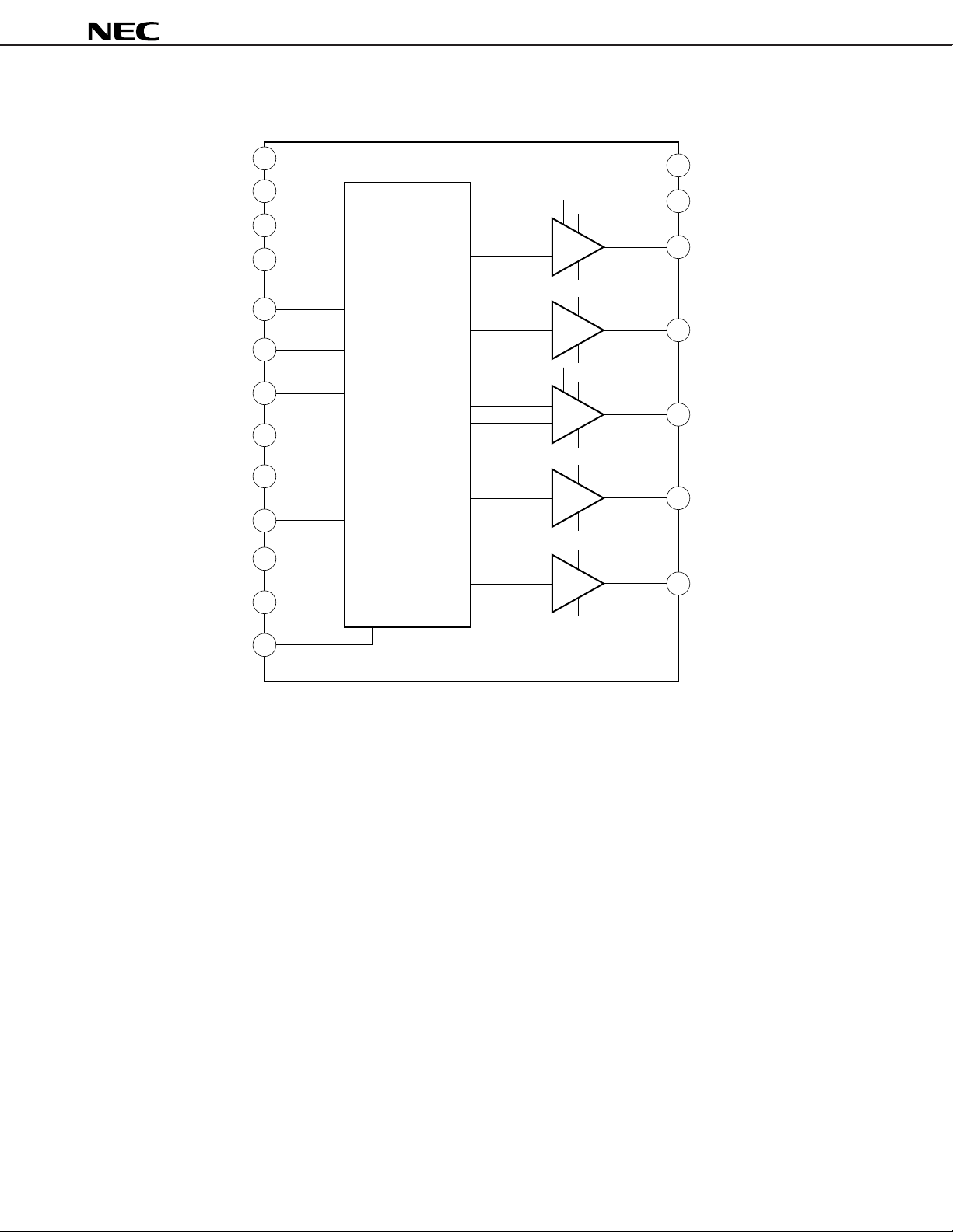
BLOCK DIAGRAM
SUBI
V
PG
PG
V
V
DD1
TI
BI
TI
BI
µ
PD16510
20
sb
16
V
DD1
V
Three
level
Two
level
Three
level
Two
level
DD2a
V
SS
DD2b
V
V
SS
DD2a
V
V
SS
DD2b
V
V
SS
SS
2
1
7
1
8
1
9
V
14
13
2
12
2
(2.0 to 5.5 V)
2
Input interface
DD1
10
19
17
18
4
V
DD2a
V
DD2b
5
TO
1
3
BO
1
TO
2
BO
2
NC
V
GND
sb
Two
level
V
1
SUBO
V
SS
11
CC
6
15
2
Page 3
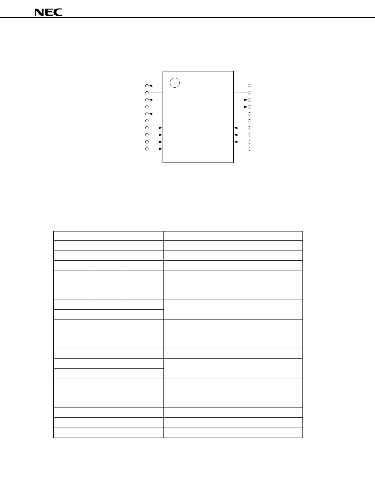
PIN CONFIGURATION
20-pin plastic shrink SOP (225 mil)
µ
PD16510
SUBO
V
BO
V
DD2a
TO
V
TI
PG
BI
SUBI
SS
1
1
CC
1
1
1
10
1
2
3
4
5
6
7
8
9
20
19
18
17
16
15
14
13
12
11
V
V
BO
TO
V
GND
TI
PG
BI
NC
Remark The µPD16510 is pin-compatible with the µPD16506 (CCD driver).
However, the VOD shutter drive pulse input polarity switching pin (SSP) of the
to the GND pin in the µPD16510 (pin 15).
PIN FUNCTIONS
No. Symbol I/O Pin Function
1 SUBO O VOD shutter drive pulse output
2VSS –VL power supply
3BO1 O Two-level pulse output
4VDD2a –VMa (Three-level driver) power supply
5TO1 O Three-level pulse output
6VCC – Logic power supply
7TI1 I Three-level driver input (See Functions table on p. 4)
8PG1 I
9BI1 I Two-level driver input (See Functions table on p. 4)
10 SUBI I VOD shutter drive pulse input
11 NC – Non connect
12 BI2 I Two-level driver input (See Functions table on p. 4)
13 PG2 I Three-level driver input (See Functions table on p. 4)
14 TI2 I
15 GND – Ground
16 VDD1 –VH power supply
17 TO2 O Three-level pulse output
18 BO2 O Two-level pulse output
19 VDD2b –VMb (Two-level driver) power supply
20 Vsb –VHH (for SUB drive) power supply
sb
DD2b
DD1
2
2
2
2
2
µ
PD16506 corresponds
3
Page 4
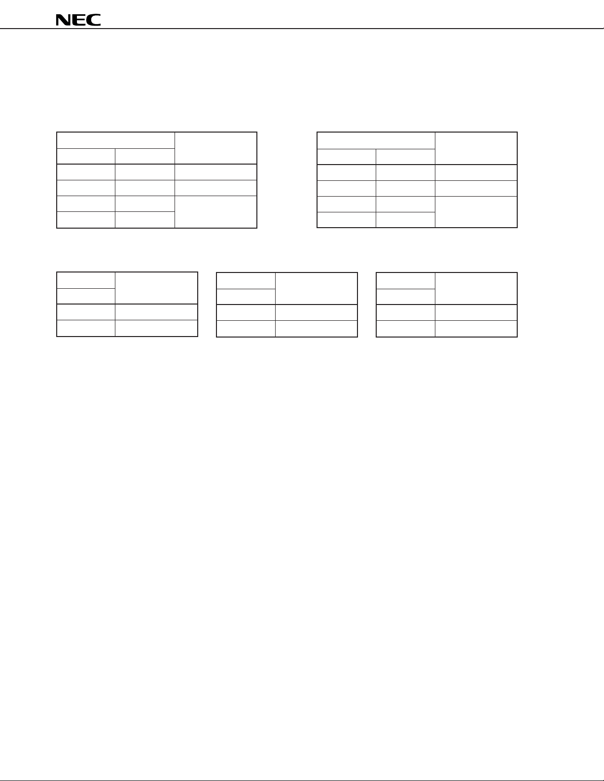
FUNCTIONS
VL = VSS, VMa = VDD2a, VMb = VDD2b, VH = VDD1, VHH = Vsb
Pin TO
1
Pin TO2
µ
PD16510
Input
TI1 PG1
LL VH
LH VMa
HL VL
HH
Output (TO1)
Pin BO1
Input
BI1
LVMb
HVL
Output (BO1)
Pin BO2
Input
BI2
LVMb
HVL
Output (BO2)
Input
TI2 PG2
LL VH
LH VMa
HL VL
HH
Output (TO2)
Pin SUBO
Input
SUBI
LVHH
HVL
Output (SUBO)
Usage Caution
Because the µPD16510 contains a PN junction (diode) between VDD2 → VDD1, if the voltage is VDD2 > VDD1, an
abnormal current will result.
Therefore, apply power in the sequence V
DD1 → VDD2, or apply power simultaneously to VDD1 and VDD2.
4
Page 5
µ
PD16510
ELECTRICAL SPECIFICATIONS
ABSOLUTE MAXIMUM RATINGS (Unless otherwise specified, TA = 25 ˚C, GND = 0 V)
Parameter Symbol Conditions Rating Unit
Power supply voltage VCC VSS–0.3 to VSS+20.0 V
Power supply voltage VDD1 VSS–0.3 to VSS+33.0 V
Power supply voltage VDD2 VSS–0.3 to VSS+33.0 V
Power supply voltage Vsb VSS–0.3 to VSS+33.0 V
Input voltage VI VSS–0.3 to VCC+0.3 V
Operating ambient temperature TA –25 to +85 °C
Storage temperature Tstg –40 to +125 °C
Power dissipation Pd TA = 85 °C 260 mW
Caution Exposure to Absolute Maximum Rating for extended periods may affect device reliability;
exceeding the ratings could cause permanent damage. The parameters apply independently.
RECOMMENDED OPERATING CONDITIONS (T
Parameter Symbol Conditions MIN. TYP. MAX. Unit
Power supply voltage VCC 2.0 5.5 V
Power supply voltage VDD1 Note 10.5 15.0 21.0 V
Power supply voltage VDD1–VSS Note 20.5 31.0 V
Power supply voltage VDD2a –1.0 +4.0 V
Power supply voltage VDD2b –1.0 +4.0 V
Power supply voltage VSS Note –10.0 –6.0 V
Power supply voltage Vsb–VSS 31.0 V
Input voltage, high VIH –0.8 VCC VCC V
Input voltage, low VIL 0 0.3 VCC V
Operating ambient temperature TA –20 +70 °C
A = 25 ˚C, GND = 0 V)
Note Set the values of VDD1 and VSS to conform to VDD1–VSS specification value.
5
Page 6

µ
ELECTRICAL CHARACTERISTICS
(Unless otherwise specified, VDD1 = +15 V, VDD2a = 0 V, VDD2b = +1.0 V, Vsb = +21.5 V, VCC = +2.5 V,
SS = –7.0 V, TA = 25 °C, GND = 0 V)
V
Parameter Symbol Conditions MIN. TYP. MAX. Unit
Output voltage, high VH IO = –20 µAVDD1–0.1 VDD1 V
Output voltage, middle VMa VDD2a–0.1 VDD2a V
Output voltage, middle VMb IO = 20 µAVDD2b–0.1 VDD2b V
Output voltage, low VL VSS+0.1 VSS V
Output voltage, sub high VsubH IO = –20 µAVsb–0.1 Vsb V
Output voltage, sub low VsubL IO = 20 µAVSS+0.1 VSS V
Output ON resistance RL IO = 10 mA 20 30 Ω
Output ON resistance RM IO = ± 10 mA 30 45 Ω
Output ON resistance RH IO = –10 mA 30 40 Ω
Output ON resistance Rsub 30 40 Ω
Transmission delay time 1
Transmission delay time 2
Transmission delay time 3
Rise/Fall time 1 TP1 See Figure 1. Output Load Circuit. 500 ns
Rise/Fall time 2 TP2 See Figure 2. Timing Chart. 500 ns
Rise/Fall time 3 TP3 200 ns
Consumption Current ICC See Figure 1. Output Load Circuit. 0.5 1.0 mA
Consumption Current IDD2a See Figure 3. Input Waveform. 3.0 5.0 mA
Consumption Current IDD2b 3.0 5.0 mA
Consumption Current lDD1 1.5 3.0 mA
Consumption Current Isb 1.2 1.8 mA
TD1 No load, see Figure 2. Timing Chart. 200 ns
TD2 200 ns
TD3 200 ns
PD16510
Figure 1. Output Load Circuit
2000 pF
1000 pF
TO1 BO2
3000 pF
1000 pF
BO1 TO2
2000 pF
2000 pF
3000 pF
SUBO
1600 pF
2000 pF
6
Page 7

BI1, BI
TI1, TI
BO1, BO
TO1, TO
µ
PD16510
Figure 2. Timing Chart
2
2
T
D1
2
2
T
P1
T
D1
V
Mb
V
Ma
V
L
T
P1
PG1, PG
TO1, TO
SUBI
SUBO
2
T
D2
2
T
P2
T
D3
T
D2
V
H
V
Ma
T
P2
T
D3
V
HH
V
L
T
P3
T
P3
7
Page 8

Input pulse timing diagram
Figure 3. Input Waveform
µ
PD16510
Tl2
Tl1
Bl1
Bl2
PG1
PG2
SUBI
µ
2 s
µ
2 s
µ
63.5 s
µ
63.5 s
µ
2.5 s
µ
127 s
µ
2.5 s
16.7 ms
Overlap section enlarged diagram
Tl1
Bl1
Tl2
Bl2
0 0.7 1.4 2.1 2.8 3.5 4.2 4.9
s
µ
8
Page 9

APPLICATION CIRCUIT EXAMPLE
V
SS
V
CC
µ
PD16510
V
sb
V
DD1
V
SUB
(substrate voltage)
CCD
0.1 F
µ
SUB
SSG
SUB
TG
V1
V2
V3
V4
0.1 F
µ
0.1 F
µ
10
1
2
3
4
5
6
7
8
9
SUBO
SS
V
BO
1
V
DD2a
TO
1
V
CC
Tl
1
PG
1
Bl
1
SUBI
V
sb
V
DD2b
BO
TO
µ
PD16510
V
DD1
GND
Tl
PG
Bl
NC
20
0.1 F
µ
1 MΩ
19
V1
18
2
17
2
V2
V3
V4
16
0.1 F
µ
15
14
2
13
2
12
2
11
9
Page 10

PACKAGE DRAWING
20 PIN PLASTIC SHRINK SOP (225mil)
µ
PD16510
20
110
GE
F
C
D
11
A
K
N
B
M
M
detail of lead end
P
H
I
J
L
NOTE
Each lead centerline is located within 0.10 mm (0.004 inch) of
its true position (T.P.) at maximum material condition.
ITEM MILLIMETERS INCHES
A
7.00 MAX.
B
0.575 MAX.
C
0.65 (T.P.)
D
E
F
G
H
I
J
K
L 0.5±0.2 0.020
M
P3˚ 3˚
+0.10
0.22
–0.05
0.1±0.1
1.45 MAX.
1.15±0.1
6.4±0.2
4.4±0.1
1.0±0.2
+0.10
0.15
–0.05
0.10
0.10N 0.004
+7˚
–3˚
0.276 MAX.
0.023 MAX.
0.026 (T.P.)
+0.004
0.009
–0.003
0.004±0.004
0.057 MAX.
+0.005
0.045
–0.004
0.252±0.008
+0.005
0.173
–0.004
+0.009
0.039
–0.008
+0.004
0.006
–0.002
+0.008
–0.009
0.004
+7˚
–3˚
P20GR-65-225C-1
10
Page 11

µ
PD16510
RECOMMENDED SOLDERING CONDITIONS
When soldering this product, it is highly recommended to observe the conditions as shown below. If other soldering
processes are used, or if the soldering is performed under different conditions, please make sure to consult with our
sales offices.
For more details, refer to our document “SEMICONDUCTOR DEVICE MOUNTING TECHNOLOGY MANUAL”
(C10535E).
Surface mount device
µ
PD16510GR-8JG: 20-pin plastic shrink SOP (225 mil)
Process Conditions Symbol
Infrared ray reflow Peak temperature: 235 °C or below (Package surface temperature), IR35-00-3
Reflow time: 30 seconds or less (at 210 °C or higher),
Maximum number of reflow processes: 3 times.
VPS Peak temperature: 215 °C or below (Package surface temperature), VP15-00-3
Reflow time: 40 seconds or less (at 200 °C or higher),
Maximum number of reflow processes: 3 times.
Wave soldering Solder temperature: 260 °C or below, Flow time: 10 seconds or less, WS60-00-1
Maximum number of flow processes: 1 time,
Pre-heating temperature: 120 °C or below (Package surface temperature).
Partial heating method Pin temperature: 300 °C or below, —
Heat time: 3 seconds or less (Per each side of the device).
Caution Apply only one kind of soldering condition to a device, except for “partial heating method”, or the
device will be damaged by heat stress.
11
Page 12

[MEMO]
µ
PD16510
12
Page 13

[MEMO]
µ
PD16510
13
Page 14

[MEMO]
µ
PD16510
14
Page 15

NOTES FOR CMOS DEVICES
1 PRECAUTION AGAINST ESD FOR SEMICONDUCTORS
Note: Strong electric field, when exposed to a MOS device, can cause destruction
of the gate oxide and ultimately degrade the device operation. Steps must
be taken to stop generation of static electricity as much as possible, and
quickly dissipate it once, when it has occurred. Environmental control must
be adequate. When it is dry, humidifier should be used. It is recommended
to avoid using insulators that easily build static electricity. Semiconductor
devices must be stored and transported in an anti-static container, static
shielding bag or conductive material. All test and measurement tools
including work bench and floor should be grounded. The operator should
be grounded using wrist strap. Semiconductor devices must not be touched
with bare hands. Similar precautions need to be taken for PW boards with
semiconductor devices on it.
µ
PD16510
2 HANDLING OF UNUSED INPUT PINS FOR CMOS
Note: No connection for CMOS device inputs can be cause of malfunction. If no
connection is provided to the input pins, it is possible that an internal input
level may be generated due to noise, etc., hence causing malfunction. CMOS
device behave differently than Bipolar or NMOS devices. Input levels of
CMOS devices must be fixed high or low by using a pull-up or pull-down
circuitry. Each unused pin should be connected to VDD or GND with a
resistor, if it is considered to have a possibility of being an output pin. All
handling related to the unused pins must be judged device by device and
related specifications governing the devices.
3 STATUS BEFORE INITIALIZATION OF MOS DEVICES
Note: Power-on does not necessarily define initial status of MOS device. Produc-
tion process of MOS does not define the initial operation status of the device.
Immediately after the power source is turned ON, the devices with reset
function have not yet been initialized. Hence, power-on does not guarantee
out-pin levels, I/O settings or contents of registers. Device is not initialized
until the reset signal is received. Reset operation must be executed immediately after power-on for devices having reset function.
15
Page 16

µ
PD16510
[MEMO]
The application circuits and their parameters are for reference only and are not intended for use in actual design-ins.
No part of this document may be copied or reproduced in any form or by any means without the prior written
consent of NEC Corporation. NEC Corporation assumes no responsibility for any errors which may appear in
this document.
NEC Corporation does not assume any liability for infringement of patents, copyrights or other intellectual property
rights of third parties by or arising from use of a device described herein or any other liability arising from use
of such device. No license, either express, implied or otherwise, is granted under any patents, copyrights or other
intellectual property rights of NEC Corporation or others.
While NEC Corporation has been making continuous effort to enhance the reliability of its semiconductor devices,
the possibility of defects cannot be eliminated entirely. To minimize risks of damage or injury to persons or
property arising from a defect in an NEC semiconductor device, customers must incorporate sufficient safety
measures in its design, such as redundancy, fire-containment, and anti-failure features.
NEC devices are classified into the following three quality grades:
"Standard", "Special", and "Specific". The Specific quality grade applies only to devices developed based on a
customer designated "quality assurance program" for a specific application. The recommended applications of
a device depend on its quality grade, as indicated below. Customers must check the quality grade of each device
before using it in a particular application.
Standard: Computers, office equipment, communications equipment, test and measurement equipment,
audio and visual equipment, home electronic appliances, machine tools, personal electronic
equipment and industrial robots
Special: Transportation equipment (automobiles, trains, ships, etc.), traffic control systems, anti-disaster
systems, anti-crime systems, safety equipment and medical equipment (not specifically designed
for life support)
Specific: Aircrafts, aerospace equipment, submersible repeaters, nuclear reactor control systems, life
support systems or medical equipment for life support, etc.
The quality grade of NEC devices is "Standard" unless otherwise specified in NEC's Data Sheets or Data Books.
If customers intend to use NEC devices for applications other than those specified for Standard quality grade,
they should contact an NEC sales representative in advance.
Anti-radioactive design is not implemented in this product.
M4 96.5
 Loading...