

Page 1
DATA SHEET
MOS INTEGRATED CIRCUIT
µ
PD16431A
1/2, 1/3, 1/4-DUTY LCD CONTROLLER/DRIVER
The µPD16431A is an LCD controller/driver that enables display of segment type LCDs of 1/2, 1/3, or 1/4 duty
cycle. This controller/driver has 56 segment output lines of which eight can also be used as LED output lines.
µ
Because the LCD driver contained in the
drive voltage can be set. In addition, key source output lines for key scanning and key input data lines are
µ
also provided, so that the
FEATURES
• Various display modes
1/2 duty: 112 segment outputs or 96 segment outputs + 8 LED outputs
1/3 duty: 168 segment outputs or 144 segment outputs + 8 LED outputs
1/4 duty: 224 segment outputs or 192 segment outputs + 8 LED outputs
• Key scan circuit (key source outputs are shared with LCD driver outputs)
• Independent LCD driver power supply V
• Serial data input/output (SCK, STB, DATA)
• On-chip oscillator incorporated
• Power-ON reset circuit
PD16431A is ideal for applications in the front panel of an automobile stereo system.
PD16431A has separate logic and power supply, up to 6.5 V of LCD
LCD (can be set to VDD to 6.5 V)
ORDERING INFORMATION
Part Number Package
µ
PD16431AGC-7ET 80-pin plastic QFP (0.65 pitch, 14 × 14)
Document No. IC-3414
(O.D. No. IC-8885)
Date Published January 1995 P
Printed in Japan
©
1995
Page 2
BLOCK DIAGRAM
µ
PD16431A
STB
DATA
CLK
Key counter
Write address
I/O
control
8-bit
shift
register
1
2
8
/KS
/KS
/KS
1
1
8
S
S
S
Level shifter (56)
Output latch (56 × 4)
56-bit shift register
Command
decoder
8
48
Segment driver
56
56
Selector circuit
56
56
Key counter
48
S
1
/LED
49
S
8
8
OE
LED
driver
2
Read
address
Key latch S/R
8
/LED
56
S
COM1COM
Common
driver
Level
shifter
Timing
generator
OSC
4
OE
4
LCD/LED
SYNC
4
OSC
IN
OSC
OUT
key
1
key
4
KEY REQ
VDDVSSV
LCDVLC1VLC2VLC3
2
Page 3
PIN CONFIGURATION
µ
PD16431A
SEG36
SEG35
SEG34
SEG33
SEG32
SEG31
SEG30
SEG29
SEG28
SEG27
SEG26
SEG25
SEG24
SEG23
SEG22
SEG21
SEG20
SEG19
SEG18
SEG17
SEG37
SEG38
SEG39
SEG40
SEG41
SEG42
SEG43
SEG44
SEG45
SEG46
SEG47
SEG48
SEG49/LED1
SEG50/LED2
SEG51/LED3
SEG52/LED4
SEG53/LED5
SEG54/LED6
SEG55/LED7
SEG56/LED8
61
80
4160
40
21
201
VSS
KEY1
KEY2
KEY3
KEY4
KEY REQ
SCK
STB
DATA
IN
OE
OSC
LCD/LED
OSCOUT
DD
V
SYNC
VLCD
VLC1
VLC2
VLC3
VEE
SEG16
SEG15
SEG14
SEG13
SEG12
SEG11
SEG10
SEG9
SEG8/KS8
SEG7/KS7
SEG6/KS6
SEG5/KS5
SEG4/KS4
SEG3/KS3
SEG2/KS2
SEG1/KS1
COM4
COM3
COM2
COM1
Note Though VSS and VEE are internally connected, be sure to connect all the power supply pins (VDD, VSS,
VLCD, and VEE).
3
Page 4
PIN FUNCTIONS
µ
PD16431A
Symbol
SEG1/KS1 to
SEG8/KS8
SEG9 to SEG48
SEG49/LED1 to
SEG56/LED8
COM1 to COM4
SCK
DATA
STB
LCD/LED
Note
OE
Name
Segment output/key
source output
Segment output
Segment output/LED
output pins
Common output
Shift clock input
Data input/output
Strobe input
LCD/LED select
Output enable input
No.
25 to 32
33 to 72
73 to 80
21 to 24
7
8
9
10
11
Description
These pins serve as LCD segment output pins and key
source output pins for key scanning.
LCD segment output pins
These pins can be used as LCD segment output or LED
output pins depending on the setting of the LCD/LED pin.
LCD common output pins
Data shift clock. Data is read at the rising edge, and is
output at the falling edge of this clock.
This pin inputs a command or display data, or outputs
key data.
A command or data is input at the rising edge of the shift
clock, starting from the most significant bit. Key data is
output at the falling edge of the shift clock, starting from
the most significant bit.
This pin serves as an open-drain pin in the output mode.
Data can be input when this signal goes low. When it
goes high, command processing is performed.
When this signal goes high, the SEGn/LEDm pins function
as LCD segment output pins; when it goes low, they
function as LED driver output pins. The LED driver has a
drive capability of 15 mA and is N-ch open drain.
When this signal goes low, all the segment output and
LED output pins are off (SEGn = COMn = VLCD). Internal
data are saved.
OSCIN
OSCOUT
SYNC
KEY1 to KEY4
KEY REQ
VDD
VSS
VLCD
VEE
VLC1 to VLC3
Oscillation input
Oscillation output
Synchronizing signal
Key data input
Key request output
Logic power supply
Logic GND
LCD drive power supply
LCD GND
Power supply for LCD
drive
12
13
14
2 to 5
6
15
1
16
20
17 to 19
Connect a resistor for oscillation circuit across these pins.
A synchronizing signal input pin. When two or more
µ
PD16431A’s are used, each device is wired-ORed. This
pin must be pulled up when this chip is used alone.
Key data input pins for key scanning
This signal goes high when a key is pressed (key data = H).
Read the key data only while this pin is high.
Power supply pin for internal logic
GND pin for internal logic and LED output
Power supply pin for LCD drive
GND pin for LCD drive
Power supply for driving dot matrix LCD
Note At OE = L, the key data cannot be written correctly, even when the display ON/OFF of the status
command is set to the “normal operation” (10). Also, in this state, unnecessary waveforms are
generated from between SEG
1/KS1 to SEG8/KS8 during the key scanning period. (The display is OFF.)
4
Page 5
µ
PD16431A
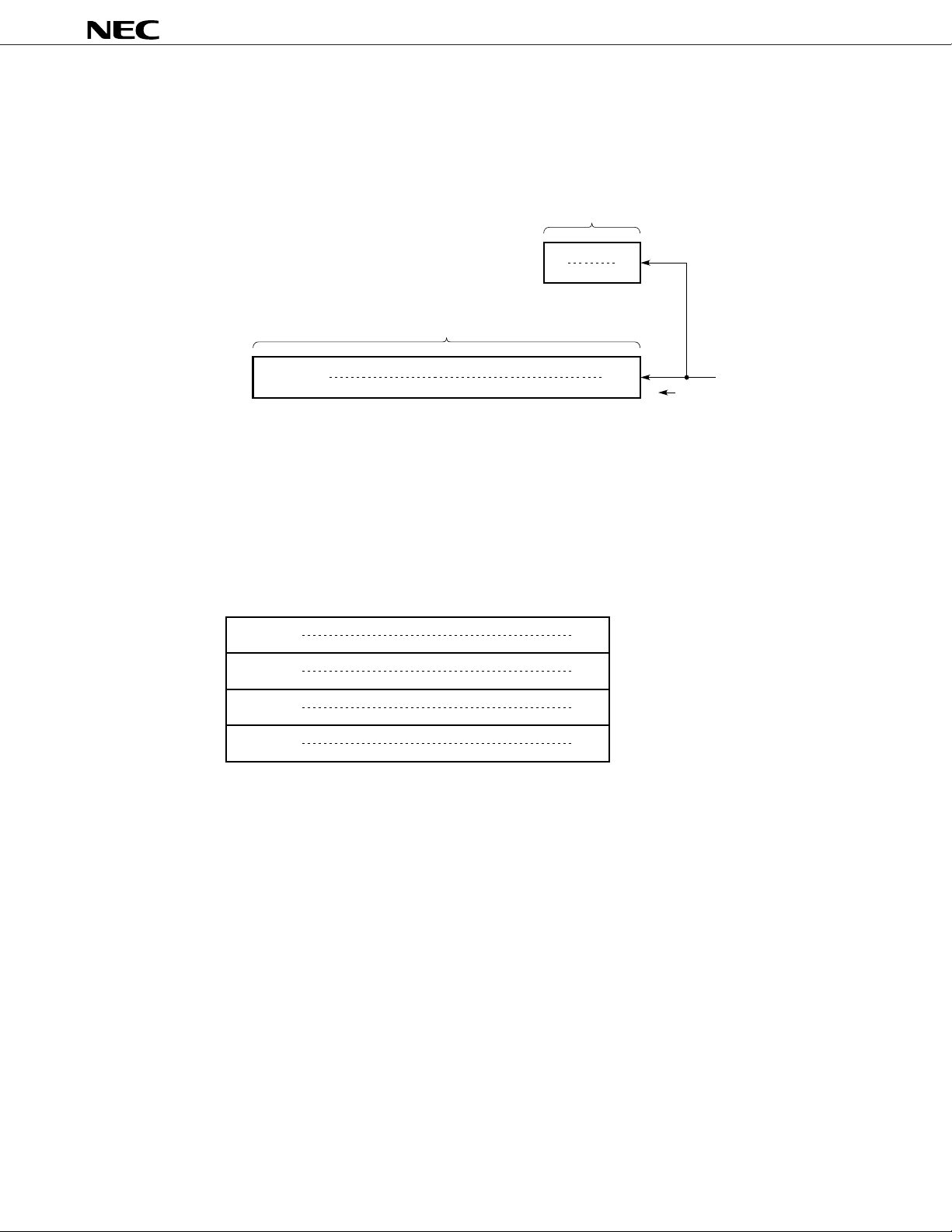
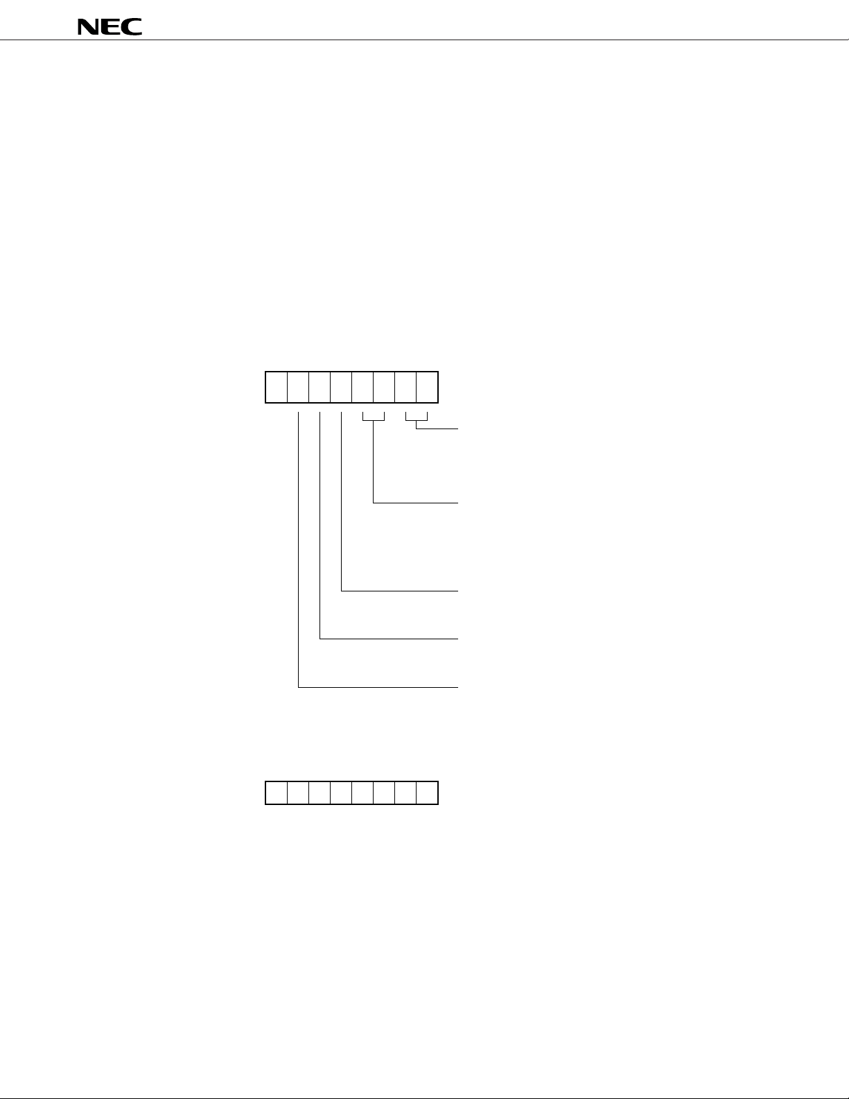
CONFIGURATION OF SHIFT REGISTER
Two shift registers, an 8-bit command register and a 56-bit display register, are provided. The first 8 bits
of input data are recognized as a command and are sent to the command register, and the 9th bit and those
that follow are recognized as display data and are sent to the display register.
8-bit shift register
MSB LSB
56-bit shift register
MSB LSB
SEG56/LED
8
Display data (LCD, LED)
The meaning of the display data is as follows:
LCD: 0 → off, 1 → on
LED: 0 → on, 1 → off
Be sure to transfer 56 bits of display data.
CONFIGURATION OF OUTPUT LATCH
MSB LSB
SEG56/LED
SEG56/LED
SEG56/LED
8
8
8
b7
b0
Command
SEG
1
SEG
1
COM1 (latch address
SEG1COM2 (latch address
SEG1COM3 (latch address
Transfer direction
Note
: 00)
Note
: 01)
Note
: 10)
SEG56/LED
8
Note Bits b3 and b4 of status command (Refer to page 8.)
SEG1COM4 (latch address
Note
: 11)
5
Page 6
KEY MATRIX CONFIGURATION
An example of key matrix configurations is shown below.
1) When pressing three or more times is assumed:
A configuration example is shown below. In this configuration, 0 to 32 ON switches can be
recognized.
µ
PD16431A
KEY1
=
KEY2
KEY3
KEY4
KS2 KS3 KS4 KS5 KS6 KS7 KS8KS1
C
2) When pressing twice or more times is assumed:
A configuration example is shown below. In this configuration, 0 to 2 ON switches can be recognized.
KEY1
=
KEY2
KEY3
KEY4
Diode A
KS2 KS3 KS4 KS5 KS6 KS7 KS8KS1
In this configuration, pressing three or more times may cause OFF switches to be determined to be ON.
For example, if SW2 to SW4 are ON and KS
1 has been selected (high level) as shown below, SW3 in which
current I1 is running is supposed to be detected to be ON. However, since SW2 and SW4 are ON, current
2 runs thus resulting in SW1 to be recognized as being ON.
I
SW1 SW2
KEY1
=
KEY2
KEY3
KEY4
I2
I1
SW3 SW4
KS2 KS3 KS4 KS5 KS6 KS7 KS8
KS1
Select
6
Page 7
µ
PD16431A
If diode A is not available, not only the key data may not be read normally but the LCD display may be
affected or ICs may be damaged or deteriorated.
For example, if SW1 and SW2 are ON and KS1 has been selected (high level) as shown below, this will
cause not only current I
1 which is supposed to run but also short-circuited current I2 of KS1 to KS2 to run.
It is possible that this will then cause the following three problems:
(1)Since the level to KEY2 is not correctly sent, the key data cannot be latched correctly.
(2)If KS
2 is used as SEG2 as well, the LCD display may be distorted (such as causing unintended segments
to light up).
(3)Since the short-circuited current (current I2) of KS2 (high level) to KS2 (low level) runs, ICS may be
damaged or deteriorated
KEY1
SW1 SW2
KEY2
I1
KEY3
KEY4
I2
=
KS2 KS3 KS4 KS5 KS6 KS7 KS8
KS1
Select
(high level)
Non Select
(low level)
7
Page 8
µ
PD16431A
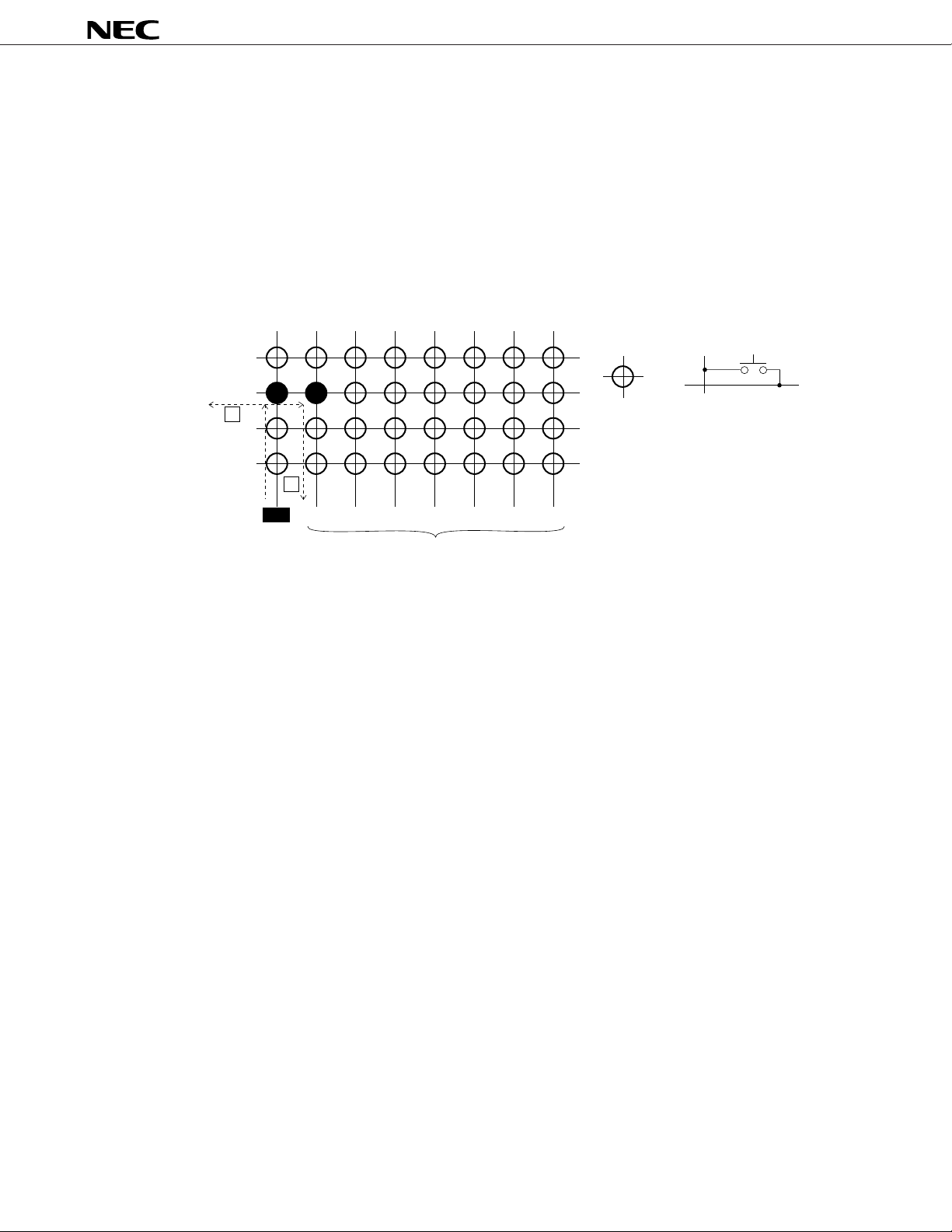
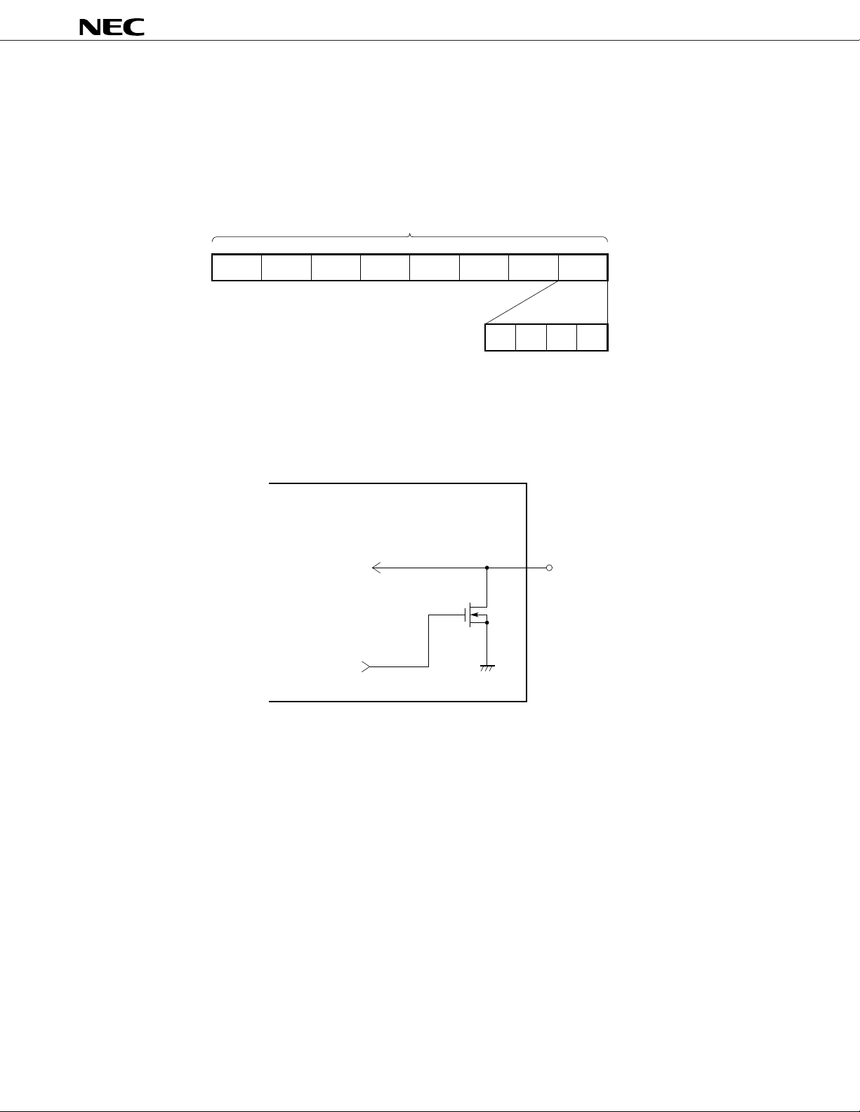
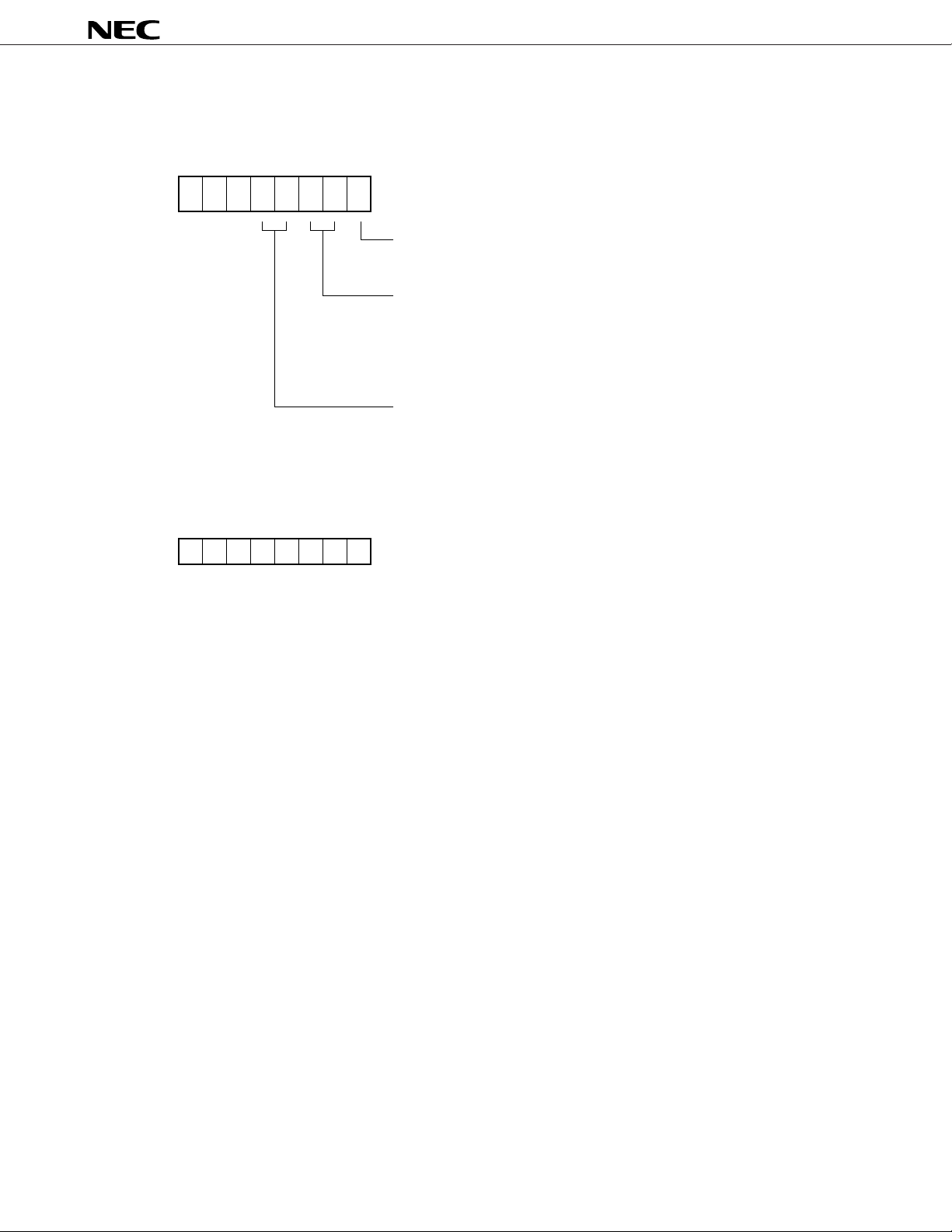
CONFIGURATION OF KEY DATA LATCH
The key data is latched as illustrated below and is read by a read command, starting from the most
significant bit. Key data is read once a frame and latched when coinciding with the immediadtely preceding
data. In other words, it requires at least 2 frames from the time the key is pressed till data is confirmed to
be the key data (the key request becoming H).
32-bit latch/SHIFT register
MSB LSB
KS
KS
8
7
The key data is 0 when off and 1 when on.
KEY INPUT EQUIVALENT CIRCUIT
Pull-down
control signal
KS
3
KEY
4
KS
KEY
KS
6
KS
5
KS
4
KS
KEY
2
1
KEY
1
2
3
KEY nTo key latch
• The pull-down control signal goes high only during key
source output and turns on the pull-down transistor.
• The on-resistance of the pull-down transistor is several kΩ.
8
Page 9
µ
PD16431A
COMMAND
A command sets a display mode and a status.
The first 1 byte input after the STB pin has fallen is regarded as a command.
If the STB pin is made low while a command/data is transferred, serial communication is initialized, and
the command/data being transferred is made invalid (the command/data that has been already transferred
remains valid, however).
(1) Display setting command
µ
This command initializes the
PD16431A and sets a duty cycle, frame frequency, drive voltage supply
method, test mode, and whether the µPD16431A operates as the master or a slave.
When this command is executed, display is forcibly turned off and key scanning is stopped. To resume
the display, the normal operation of the “status command” must be executed. Note, however, that nothing
is executed if the same mode is selected.
MSB LSB
b0
b1b2b3b4b5b60
Sets duty.
00: 1/4 duty, 1/3 bias
01: 1/3 duty, 1/3 bias
10: 1/2 duty, 1/2 bias
11: 1/2 duty, 1/2 bias
Sets frame frequency.
OSC
/128) × n
00: (f
01: (f
OSC
/256) × n
OSC
/512) × n
10: (f
11: (f
OSC
/1024) × n
n= duty (1/2, 1/3, 1/4)
Sets drive voltage supply method.
0: Internal
1: External
Sets master or slave.
0: Master
1: Slave
Sets test mode.
0: Normal operation
1: Test mode
Values when power is applied
0
000000
9
Page 10
(2) Status command
This command sets a data write/read mode, turns on/off display, and sets a latch address.
MSB LSB
µ
PD16431A
Values when power is applied
b0
b1b2b3b4××1
0
0000××
× : Don’t Care
Sets data write/read mode.
0: Writes display data to output latch
1: Reads key data
Turns on/off display
00: Forcibly turns off display (all segments and LEDs off).
Stops key scanning.
01: Prohibited
10: Normal operation
11: Don’t care
Sets latch address.
00: COM
01: COM
10: COM
11: COM
1
2
3
4
10
Page 11
OUTPUT SELECT VOLTAGE
1. COM
+ – Bias
When selected VLCD GND 1/2 bias
VLCD GND
When not selected 1/2 VLCD 1/2 VLCD
VLC2 VLC2
When key scanned 1/2 VLCD 1/2 VLCD
VLC2 VLC2
When selected VLCD GND 1/3 bias
VLCD GND
When not selected 1/3 VLCD 2/3 VLCD
VLC3 VLC1
When key scanned 1/2 VLCD 1/2 VLCD
VLC2 VLC2
µ
PD16431A
Top : with internal power supply
Bottom: with external power supply
2. SEG
+ – Bias
When selected GND VLCD 1/2 bias
GND VLCD
When not selected VLCD GND
VLCD GND
When key scanned GND VLCD
GND VLCD
When key not VLCD GND
scanned VLCD GND
When selected GND VLCD 1/3 bias
GND VLCD
When not selected 2/3 VLCD 1/3 VLCD
VLC1 VLC3
When key scanned GND VLCD
GND VLCD
When key not VLCD GND
scanned VLCD GND
11
Page 12

OUTPUT WAVEFORM
(1) 1/2 duty (1/2 dias)
µ
PD16431A
COM1
COM2
SEG1
SEG9
VLCD
VLC2
VEE
VLCD
VLC2
VEE
VLCD
VLC2
VEE
VLCD
VLC2
VEE
VLCD
*
K
0
*
0101
K
1
*
K
0
*
K
1
*
K
0
*: key scan period (16/fc)
1/2VLCD
SEG1-COM1
-1/2V
1/2VLCD
SEG1-COM2
-1/2VLCD
1 KEY REQ
(w/key)
2 KEY REQ
(w/key→w/o key)
3 KEY REQ
(w/o key→w/key)
0
LCD
-VLCD
VLCD
0
-VLCD
12
Page 13

KEY SCAN PERIOD (K0) EXPANSION
1K0 0
1 2345678
LCD
V
V
COM
SEG
LC2
1
V
EE
V
LCD
V
LC2
1
V
EE
V
LCD
µ
PD16431A
SEG
SEG
SEG
SEG5-SEG
V
LC2
2
V
EE
V
LCD
V
LC2
3
V
EE
V
LCD
V
LC2
4
V
EE
V
LCD
V
LC2
40
V
EE
= Key source output
13
Page 14

KEY SCAN PERIOD (K1) EXPANSION
0K1 1
1 2345678
V
LCD
µ
PD16431A
COM1
SEG1-SEG4,
SEG9-SEG40
SEG5
SEG6
SEG7
VLC2
VEE
VLCD
VLC2
VEE
VLCD
VLC2
VEE
VLCD
VLC2
VEE
VLCD
VLC2
VEE
VLCD
14
SEG8
1 KEY REQ
(w/key)
2 KEY REQ
(w/key→w/o key)
3 KEY REQ
(w/o key→w/key)
VLC2
VEE
= Key source output
Page 15

(2) 1/3 duty (1/3 bias)
µ
PD16431A
COM
COM
COM
SEG
SEG
V
V
V
1
V
V
V
V
2
V
V
V
V
3
V
V
V
V
1
V
V
V
V
9
V
LCD
LC1
LC2
LC3
V
LCD
LC1
LC2
LC3
V
LCD
LC1
LC2
LC3
V
LCD
LC1
LC2
LC3
V
LCD
LC1
LC2
LC3
V
*
K
0
EE
EE
EE
EE
EE
*
0120
K
1
*
K
2
*
K
0
*
K
1
*: key scan period (16/fc)
SEG
SEG
1
-COM
1
-COM
1
2
1/2V
1/3V
-1/3V
-1/2V
1/2V
1/3V
-1/3V
-1/2V
V
LCD
LCD
LCD
0
LCD
LCD
-V
LCD
V
LCD
LCD
LCD
0
LCD
LCD
-V
LCD
15
Page 16

KEY SCAN PERIOD (K0) EXPANSION
2K0 0
1 2345678
V
LCD
LC1
V
V
COM
SEG
SEG
LC2
1
V
LC3
V
EE
V
LCD
V
LC1
V
LC2
1
V
LC3
V
EE
V
LCD
V
LC1
V
LC2
2
V
LC3
V
EE
µ
PD16431A
SEG
SEG
SEG5-SEG
V
LCD
V
LC1
V
LC2
3
V
LC3
V
EE
V
LCD
V
LC1
V
LC2
4
V
LC3
V
EE
V
LCD
V
LC1
V
LC2
8
V
LC3
V
EE
= Key source output
16
Page 17

KEY SCAN PERIOD (K1) EXPANSION
0K1 1
1 2345678
V
LCD
V
LC1
V
COM
SEG1-SEG
SEG9-SEG
SEG
LC2
1
V
LC3
V
EE
V
LCD
V
LC1
V
LC2
4,
40
V
LC3
V
EE
V
LCD
V
LC1
V
LC2
5
V
LC3
V
EE
µ
PD16431A
SEG
SEG
SEG
V
LCD
V
LC1
V
LC2
6
V
LC3
V
EE
V
LCD
V
LC1
V
LC2
7
V
LC3
V
EE
V
LCD
V
LC1
V
LC2
8
V
LC3
V
EE
= Key source output
17
Page 18

KEY SCAN PERIOD (K2) EXPANSION
1K2 2
1 2345678
VLCD
VLC1
COM1
SEG1-SEG40
VLC2
VLC3
VEE
VLCD
VLC1
VLC2
VLC3
VEE
µ
PD16431A
18
Page 19

(3) 1/4 duty (1/3 bias)
µ
PD16431A
COM1
COM2
COM3
COM4
SEG1
VLCD
VLC1
VLC2
VLC3
VEE
VLCD
VLC1
VLC2
VLC3
VEE
VLCD
VLC1
VLC2
VLC3
VEE
VLCD
VLC1
VLC2
VLC3
VEE
VLCD
VLC1
VLC2
VLC3
VEE
*
K
0
*
0123
K
1
*
K
2
*
K
3
*
K
0
*
0
K
1
*: key scan period
(16/fc)
SEG
SEG
SEG9
1-COM1
1-COM2
VLCD
VLC1
VLC2
VLC3
VEE
VLCD
2/3V
LCD
1/2VLCD
1/3VLCD
-1/3VLCD
-1/2VLCD
-2/3VLCD
-VLCD
VLCD
2/3VLCD
1/2VLCD
1/3VLCD
-1/3VLCD
-1/2VLCD
-2/3VLCD
-VLCD
0
0
19
Page 20

KEY SCAN PERIOD (K0) EXPANSION
3K0 0
1 2345678
LCD
V
V
LC1
V
COM
SEG
SEG
LC2
1
V
LC3
V
EE
V
LCD
V
LC1
V
LC2
1
V
LC3
V
EE
V
LCD
V
LC1
V
LC2
2
V
LC3
V
EE
µ
PD16431A
SEG
SEG
SEG5-SEG
V
LCD
V
LC1
V
LC2
3
V
LC3
V
EE
V
LCD
V
LC1
V
LC2
4
V
LC3
V
EE
V
LCD
V
LC1
V
LC2
40
V
LC3
V
EE
= Key source output
20
Page 21

KEY SCAN PERIOD (K1) EXPANSION
0K1 1
1 2345678
LCD
V
V
LC1
V
COM
SEG1-SEG
SEG9-SEG
SEG
LC2
1
V
LC3
V
EE
V
LCD
V
LC1
V
LC2
4,
40
V
LC3
V
EE
V
LCD
V
LC1
V
LC2
5
V
LC3
V
EE
µ
PD16431A
SEG
SEG
SEG
V
LCD
V
LC1
V
LC2
6
V
LC3
V
EE
V
LCD
V
LC1
V
LC2
7
V
LC3
V
EE
V
LCD
V
LC1
V
LC2
8
V
LC3
V
EE
= Key source output
21
Page 22

KEY SCAN PERIOD (K2) EXPANSION
VLCD
VLC1
COM1
SEG1-SEG40
VLC2
VLC3
VEE
VLCD
VLC1
VLC2
VLC3
VEE
KEY SCAN PERIOD (K3) EXPANSION
1K2 2
1 2345678
µ
PD16431A
COM1
SEG1-SEG40
2K3 3
1 2345678
VLCD
VLC1
VLC2
VLC3
VEE
VLCD
VLC1
VLC2
VLC3
VEE
22
Page 23

SERIAL COMMUNICATION FORMAT
(1) Receive (command/data write)
STB
µ
PD16431A
If data continues
DATA
SCK 123 678
b7 b6 b5 b2 b1 b0
(2) Transmit (command/data read)
STB
DATA
SCK 123
7 6 5
Data read command set Wait time tWAIT Data read
21
678
1 s
µ
76
123
43
50
456
Note Because the DATA pin is an N-ch open-drain output pin, be sure to connect an external pull-up
resistor to this pin (1 kΩ to 10 kΩ).
23
Page 24

APPLICATION
1. Example of initial setting + display data write
µ
PD16431A
Parameter STB
Start H
Set display command L 00000000 1/4 duty, frame frequency = fosc/128 × 1/4, internal drive
H
Status command L 1 0 0 0 0 0 0 0 Display data write, display off, latch address: COM1
Display data 1 L ЧЧЧЧЧЧЧЧ
Display data 7 L × × × × × × × ×
H
Status command L 1 0 0 0 1 0 0 0 Display data write, display off, latch address: COM2
Display data 1 L ЧЧЧЧЧЧЧЧ
Display data 7 L × × × × × × × ×
H
Status command L 1 0 0 1 0 0 0 0 Display data write, display off, latch address: COM3
Display data 1 L ЧЧЧЧЧЧЧЧ
Display data 7 L × × × × × × × ×
H
Status command L 1 0 0 1 1 0 0 0 Display data write, display off, latch address: COM4
Display data 1 L ЧЧЧЧЧЧЧЧ
Display data 7 L × × × × × × × ×
H
Status command L 1 0 0 0 0 1 0 0 Display data write, display on
End H
Command/data
b7 b6 b5 b4 b3 b2 b1 b0
voltage, master
COM1 data (7 bytes)
COM2 data (7 bytes)
COM3 data (7 bytes)
COM4 data (7 bytes)
Remarks
24
Page 25

2. Example of display data write (rewrite, 1/4)
µ
PD16431A
Parameter STB
Start H
Status command L 1 0 0 0 0 1 0 0 Display data write, display on, latch address: COM1
Display data 1 L ЧЧЧЧЧЧЧЧ
Display data 7 L × × × × × × × ×
H
Status command L 1 0 0 0 1 1 0 0 Display data write, display on, latch address: COM2
Display data 1 L ЧЧЧЧЧЧЧЧ
Display data 7 L × × × × × × × ×
H
Status command L 1 0 0 1 0 1 0 0 Display data write, display on, latch address: COM3
Display data 1 L ЧЧЧЧЧЧЧЧ
Display data 7 L × × × × × × × ×
H
Status command L 1 0 0 1 1 1 0 0 Display data write, display on, latch address: COM4
Display data 1 L ЧЧЧЧЧЧЧЧ
Display data 7 L × × × × × × × ×
End H
Command/data
b7 b6 b5 b4 b3 b2 b1 b0
COM1 data (7 bytes)
COM2 data (7 bytes)
COM3 data (7 bytes)
COM4 data (7 bytes)
Remarks
25
Page 26

3. Example of key data read
µ
PD16431A
Parameter STB
KEY REQ check KEY REQ = H: Key data exists. → Start reading.
Start H
Status command L 1 0 0 0 0 1 0 1 Data read, display on
Wait time L 1 µs
Key data 1 L ЧЧЧЧЧЧЧЧ
Key data 4 L × × × × × × × ×
End H
Command/data
b7 b6 b5 b4 b3 b2 b1 b0
KEY REQ = L:
4 bytes
Remarks
Key data does not exist (reading is inhibited).
→ Check KEY REQ again.
26
Page 27

µ
PD16431A
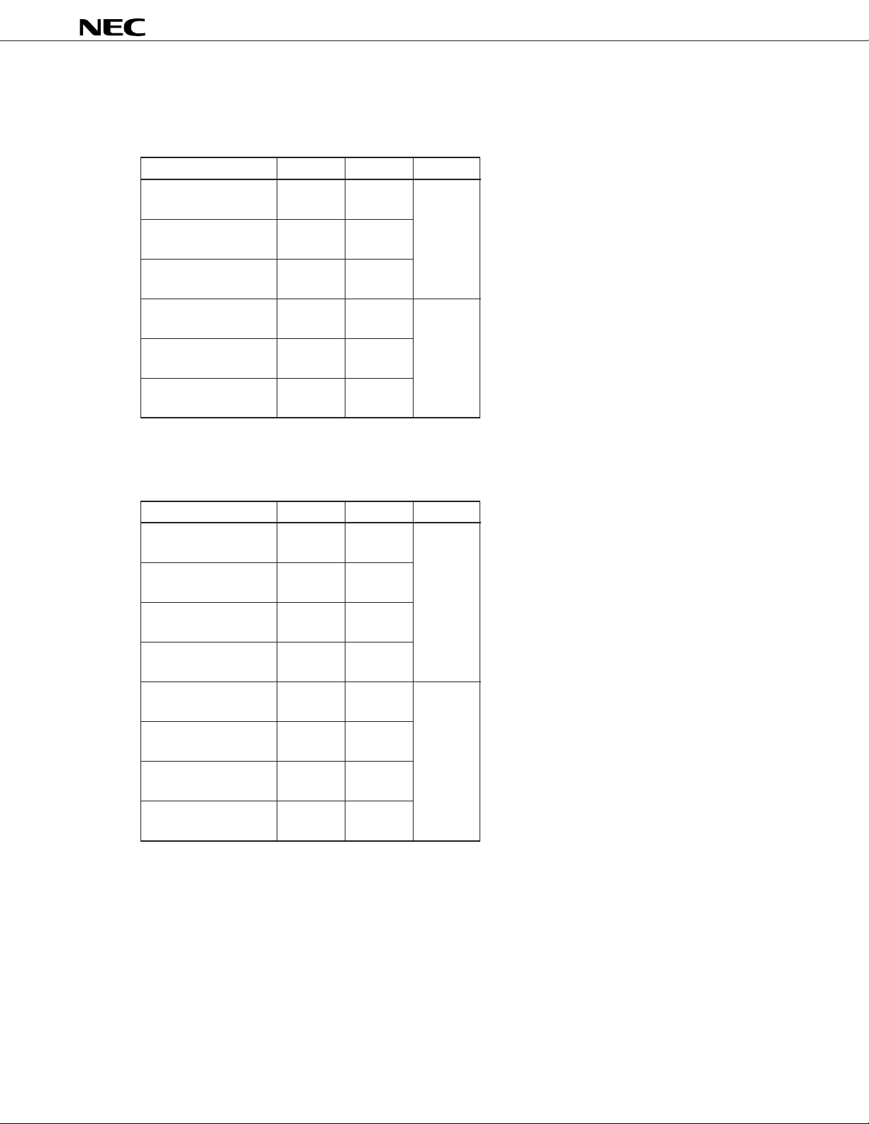
ABSOLUTE MAXIMUM RATINGS (Ta = 25 ˚C, VSS = 0 V)
Parameter Symbol Ratings Unit
Logic supply voltage VDD –0.3 to +7.0 V
Logic input voltage VIN –0.3 to VDD + 0.3 V
Logic output voltage (DATA) VOUT –0.3 to +7.0 V
LCD drive supply voltage VLCD –0.3 to +7.0 V
LCD drive supply input voltage VLC1 to VLC3 –0.3 to VLCD + 0.3 V
Driver output voltage VOUT2 –0.3 to VLCD + 0.3 V
(segment, common, LED)
LED output current IO +20 mA
Operating ambient temperature Topt –40 to +85 ˚C
Storage temperature Tstg –55 to +150 ˚C
Permissible package power PT 1 000 mW
dissipation
RECOMMENDED OPERATING CONDITIONS
Parameter Symbol MIN. TYP. MAX. Unit
Logic supply voltage VDD 2.7 5.0 5.5 V
LCD drive supply voltage VLCD VDD 5.0 6.5 V
Logic input voltage VIN 0 VDD V
Driver output voltage VLC1 to VLC3 0VLCD V
27
Page 28

µ
PD16431A
ELECTRICAL SPECIFICATIONS (Unless otherwise specified, Ta = –40 to +85 ˚C, VDD = VLCD = 5 V ±10%)
Parameter Symbol MIN. TYP. MAX. Unit
Input voltage, high VIH 0.7 VDD VDD V
Input voltage, low VIL 0 0.3 VDD V
Input current, high I
Input current, low I
IH
IL
Output voltage, low VOL1 LED1 to LED8. IOL1 = 15 mA 1.0 V
Output voltage, high VOH2 OSCOUT, IOH2 = –1 mA 0.9 VDD V
Output voltage, low VOL2 DATA, OSCOUT, SYNC, IOL2 = 4 mA 0.1 VDD V
Leakage current, high ILOH2 DATA, SYNC, VIN OUT = VDD 1 mA
Leakage current, low ILOL2 DATA, SYNC, VIN OUT = VSS –1 mA
Common output ON resistance R
Segment output ON resistance R
Logic current dissipation I
LCD drive current consumption I
COM
SEG
DD
LCD
CLK, STB, LCD/LED, OE 1
CLK, STB, LCD/LED, OE –1
COM1 to COM4, | IO | = 100
SEG1 to SEG56, | IO | = 100
f
= 250 kHz 250
OSC
µ
A 2.4 kΩ
µ
A 4.0 kΩ
With internal bias and no load 500
µ
A
µ
A
µ
A
µ
A
Remark The TYP. value is a reference value at Ta = 25 ˚C.
28
Page 29

µ
PD16431A
SWITCHING CHARACTERISTICS
(Unless otherwise specified, Ta = –40 to +85 ˚C, VDD = VLCD = 5 V ±10%, RL = 5 kΩ, CL = 150 pF)
Parameter Symbol Conditions MIN. TYP. MAX. Unit
Oscillation frequency f
Oscillation frequency f
Propagation delay time t
Propagation delay time t
SYNC delay time t
OSC
OSC
PZL
PLZ
DSYNC
R = 100 kΩ 175 250 325 kHz
R = 200 kΩ 105 150 195 kHz
SCK ↓ → DATA ↓ 100 ns
SCK ↓ → DATA ↑ 300 ns
1.5
TIMING REQUIREMENTS
(Unless otherwise specified, Ta = –40 to +85 ˚C, VDD = VLCD = 5 V ±10%, RL = 5 kΩ, CL = 150 pF)
Parameter Symbol Conditions MIN. TYP. MAX. Unit
Clock frequency fC OSCIN external clock 50 325 kHz
High-level clock pulse width t
Low-level clock pulse width t
WHC
WLC
OSCIN external clock 1.5 16
OSCIN external clock 1.5 16
µ
s
µ
s
µ
s
Shift clock cycle tCYK SCK 900 ns
High-level shift clock pulse tWHK SCK 400 ns
width
Low-level shift clock pulse tWLK SCK 400 ns
width
Shift clock hold time t
Data setup time t
Data hold time t
STB hold time t
STB pulse width t
Wait time t
HSTBK
DS
DH
DKSTB
WSTB
WAIT
STB ↓ → SCK ↓ 1.5
DATA → SCK ↑ 100 ns
SCK ↑ → DATA 200 ns
SCK ↑ → STB ↑ 1
1
CLK ↑ → CLK ↓ 1
SYNC removal time tSREM 250 ns
Output Load
VDD
5 kΩ
µ
s
µ
s
µ
s
µ
s
OUTPUT
150 pF
29
Page 30

Switching Characteristic Waveform
CSCIN
VIL
tWLC
VIH
1/fc
tWHC
µ
PD16431A
t
WSTB
STB
SCK
DATA
f
OSC
VIL
tHKSTB
tCYK
t
WHKtWLK
VIH
VIL
tDHtDS
VIH
VIL
SYNC timing (master) SYNC timing (slave)
1 frame 1 frame 1 frame 1 frame
VIH
Internal reset
30
SYNC
DSYNC tSREM
t
Page 31

Switching Characteristic Waveform
SCK
V
IL
t
PZL
DATA
V
OL2
Application Circuit Example (with LED, 1/4 duty, 1/3 bias)
µ
PD16431A
t
PLZ
LCD
To microcomputer
R
4
n
COM
2
8 40
SEG1/KS
1
SEG
to
8
/KS
SEG
SEG
8
9
to
48
V
LCD
R
8
8
Key matrix
8 × 4
LED
LED
n
KEY
n
V
EE
R
2
R
1
GND+6 V
8
4
R
1
: 1 k to 10 kΩ
R
2
R
R
R
R
: 1/2 R1
5
, R
6
: 1 k to 10 kΩ
7
: 100 kΩ TYP.
8
: 330 to 1 kΩ
1
through R2 are not necessary when
the internal drive voltage is selected
(V
LC1
through V
LC3
are open).
V
DD
R
5
V
DD
R
6
DATA
SCK
STB
KEY REQ
OE
LCD/LED
µ
PD16431A
SYNC.
OSC
IN
R
7
OSC
OUT
VDDV
SSVLCDVLC1VLC2VLC3
R
1
+5 V GND
31
Page 32

µ
PD16431A
Note Example of external source circuit (when 1/2 bias)
VDDV
SS
V
LC0
V
LC1
V
LC2
V
LC3
V
EE
R
1
R
1
R
1
+5 V GND +6 V GND
The application circuits and their parameters are for references only and are not intended for use in actual design-in's.
= 1 k to 10 kΩ
(approx.)
32
Page 33

80 PIN PLASTIC LQFP ( 14)
µ
PD16431A
A
B
4160
4061
detail of lead end
2180
F
G
H
M
IJ
201
K
P
NOTE
N
Each lead centerline is located within 0.13 mm (0.005 inch) of
its true position (T.P.) at maximum material condition.
L
C
D
S
M
ITEM MILLIMETERS INCHES
Q
A 16.0±0.2 0.630±0.008
B 14.0±0.1 0.551
C 14.0±0.1 0.551
D
F
G
H 0.30±0.10 0.012
I
J
K
L 0.5±0.2 0.020
M 0.125 0.005
N 0.10
P 1.4±0.1 0.055±0.004
Q
R3° 3°
S 1.7 MAX.
R
+0.005
–0.004
+0.005
–0.004
16.0±0.2
0.825
0.825
0.13
0.65 (T.P.)
1.0±0.2
+0.10
–0.05
0.125±0.075 0.005±0.003
+7°
–3°
0.630±0.008
0.032
0.032
+0.004
–0.005
0.005
0.026 (T.P.)
+0.009
0.039
–0.008
+0.008
–0.009
+0.004
–0.002
0.004
+7°
–3°
0.067 MAX.
S80GC-65-7ET-1
33
Page 34

µ
PD16431A
REFERENCE
Document Name Document No.
NEC Semiconductor Device Reliability/Quality Control System IEI-1212
Quality grade on NEC Semiconductor Devices IEI-1209
No part of this document may be copied or reproduced in any form or by any means without the prior written
consent of NEC Corporation. NEC Corporation assumes no responsibility for any errors which may appear in this
document.
NEC Corporation does not assume any liability for infringement of patents, copyrights or other intellectual
property rights of third parties by or arising from use of a device described herein or any other liability arising
from use of such device. No license, either express, implied or otherwise, is granted under any patents,
copyrights or other intellectual property rights of NEC Corporation or others.
While NEC Corporation has been making continuous effort to enhance the reliability of its semiconductor devices,
the possibility of defects cannot be eliminated entirely. To minimize risks of damage or injury to persons or
property arising from a defect in an NEC semiconductor device, customer must incorporate sufficient safety
measures in its design, such as redundancy, fire-containment, and anti-failure features.
NEC devices are classified into the following three quality grades:
“Standard“, “Special“, and “Specific“. The Specific quality grade applies only to devices developed based on
a customer designated “quality assurance program“ for a specific application. The recommended applications
of a device depend on its quality grade, as indicated below. Customers must check the quality grade of each
device before using it in a particular application.
Standard: Computers, office equipment, communications equipment, test and measurement equipment,
audio and visual equipment, home electronic appliances, machine tools, personal electronic
equipment and industrial robots
Special: Transportation equipment (automobiles, trains, ships, etc.), traffic control systems, anti-disaster
systems, anti-crime systems, safety equipment and medical equipment (not specifically designed
for life support)
Specific: Aircrafts, aerospace equipment, submersible repeaters, nuclear reactor control systems, life
support systems or medical equipment for life support, etc.
The quality grade of NEC devices in “Standard“ unless otherwise specified in NEC's Data Sheets or Data Books.
If customers intend to use NEC devices for applications other than those specified for Standard quality grade,
they should contact NEC Sales Representative in advance.
Anti-radioactive design is not implemented in this product.
34
M4 94.11
 Loading...