

Page 1
DATA SHEET
MOS INTEGRATED CIRCUIT
µµ
µ
PD16334
µµ
96-Bit AC-PDP DRIVER
The µPD16334 is a high-voltage CMOS driver designed for flat display panels such as PDPs, VFDs and ELs. It
consists of a 96-bit bi-directional shift register, 96-bit latch and high-voltage CMOS driver. The logic block is designed
to operate using a 5-V power supply/3.3-V interface enabling direct connection to a gate array or a microcontroller.
µ
In addition, the
withstand voltage output (80 V, 50 mA).
FEATURES
•Selectable by IBS pin; three 32-bit bi-directional shift register circuits
configuration or six 16-bit bi-directional shift register circuits configuration
•Data control with transfer clock (external) and latch
•High-speed data transfer(f
•High withstand output voltage (80 V, 50 mA
•3.3 V CMOS input interface
•High withstand voltage CMOS structure
•Capable of reversing all driver outputs by PC pin
PD16334 achieves low power dissipation by employing the CMOS structure while having a high
max. = 25 MHz min. at data fetch)
(fmax. = 15 MHz min. at cascade connection)
MAX.)
ORDERING INFORMATION
Part Number Package
µ
PD16334 COB*
* Please consult with an NEC sales representative about COB.
DocumentNo. S12362EJ2V0DS00 (2nd edition)
Date Published May 1998 N CP(K)
Printed in Japan
©
1997
Page 2
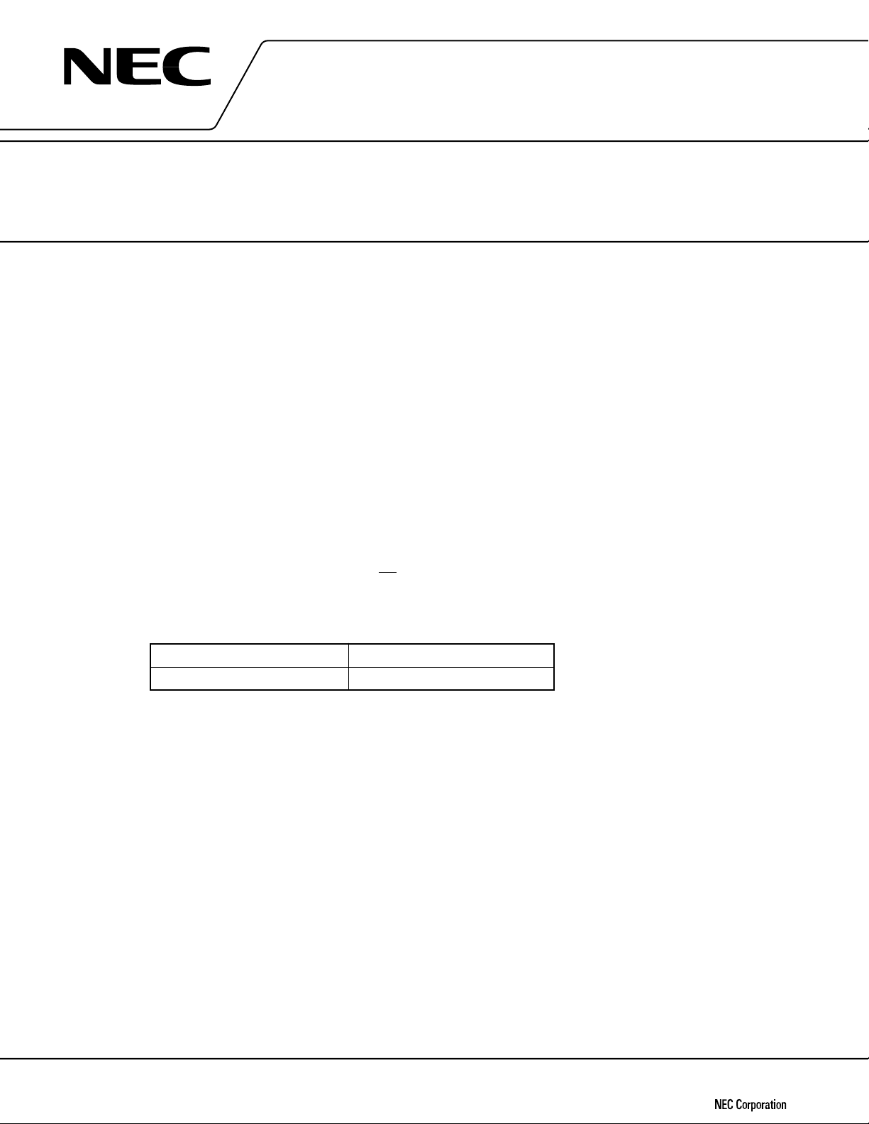
BLOCK DIAGRAM (IBS = H, 3-BIT INPUT, 32-BIT LENGTH SHIFT REGISTER)
OE
PC
BLK
LE
SR1
S
1
A
CLK
A
CLK
1
1
S
4
S
1
L
1
S
2
S
3
µµ
µ
µµ
V
DD2
PD16334
O
1
R/L
B
A
B
A
B
1
2
2
3
3
SRn: 32-bit shift register
R/L
1
B
A
2
CLK
R/L
B
2
A
3
CLK
R/L
3
B
SR2
SR3
V
SS2
S
94
S
2
S
5
S
95
S
3
S
6
94
S
S
95
S
S
96
96
L
96
V
DD2
O
96
V
SS2
2
Page 3
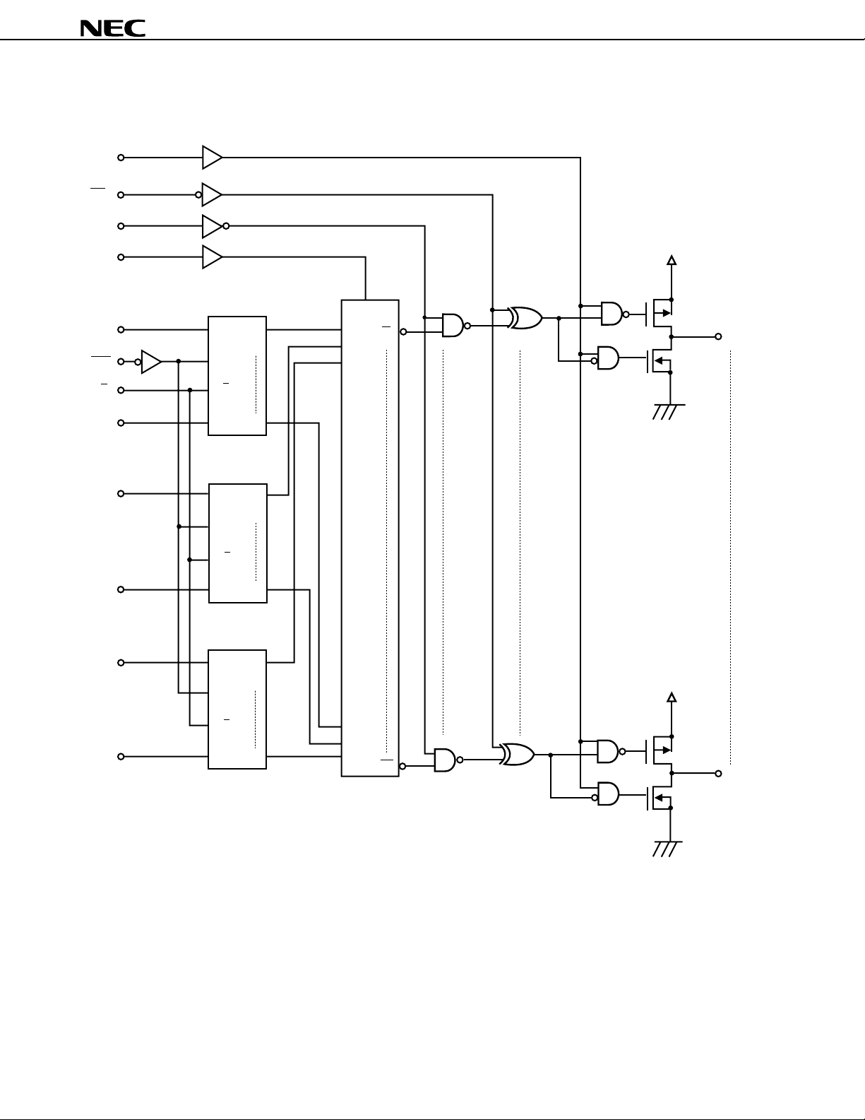
BLOCK DIAGRAM (IBS = L, 6-BIT INPUT, 16-BIT LENGTH SHIFT REGISTER)
OE
PC
BLK
LE
µµ
µ
PD16334
µµ
V
DD2
A
CLK
R/L
B
A
B
A
B
A
B
A
B
A
B
1
1
2
2
A
1
CLK
R/L
1
B
A
2
CLK
R/L
B
2
SR1
SR2
S
1
S
7
S
91
S
2
S
8
S
92
S1 LE
S
2
S
3
S
4
S
5
S
6
L
1
O
1
V
SS2
SR3
3
3
A
3
CLK
R/L
B
3
S
3
S
9
S
93
SR4
4
4
A
4
CLK
R/L
4
B
S
4
S
10
S
94
SR5
5
5
6
6
A
5
CLK
R/L
B
5
A
6
CLK
R/L
B
6
SR6
S
5
S
11
S
95
S
S
6
S
12
S
96
93
S
94
S
95
L
96
S
96
V
DD2
O
96
SRn: 16-bit shift register
V
SS2
3
Page 4
µµ
µ
PD16334
µµ
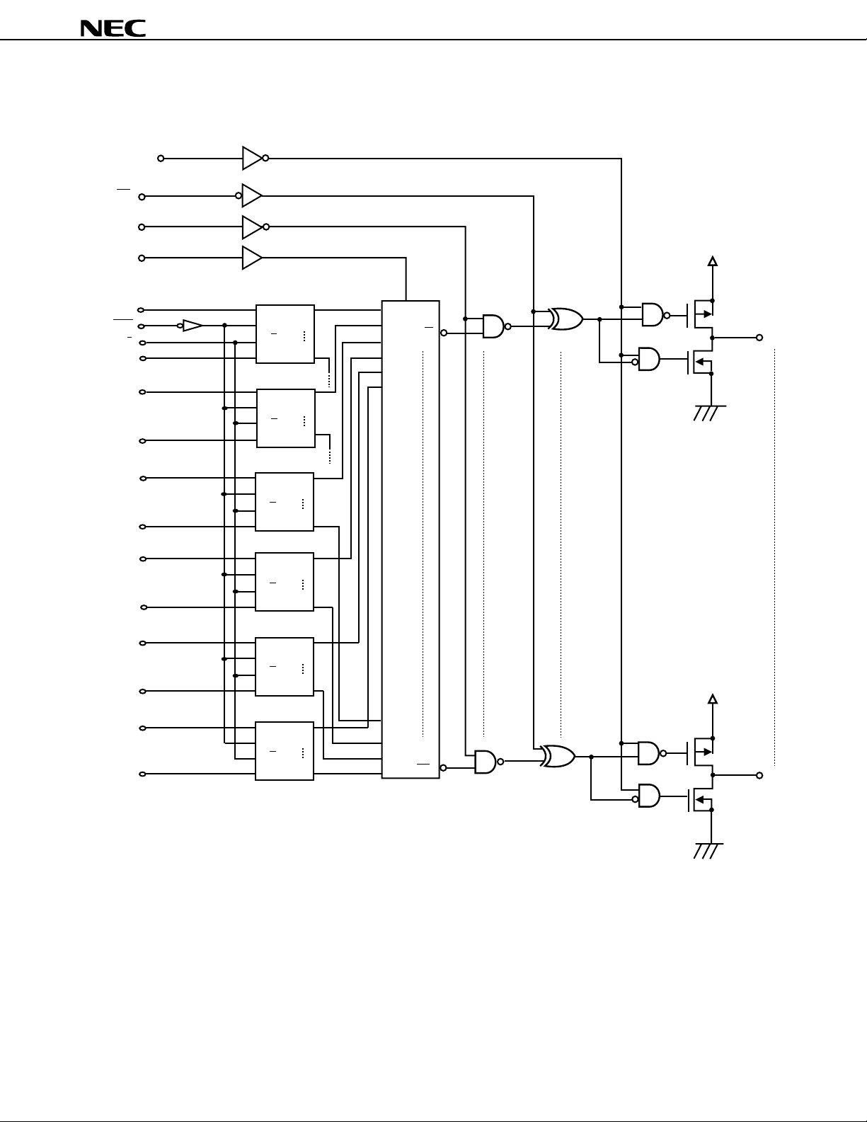
PIN DESCRIPTION
Symbol Pin Name Description
PC Polarity change input PC = L: All driver output invert
BLK Blank input BLK = H : All output = H or L
LE Latch enable input Automatically executes latch by setting high at rising edge
of the clock
OE Output enable Make output high impedance by input H
(Note)
(Note)
When R/L=H (values in parentheses are for 6-bit input)
A1 to A3 (6) : Input B1 to B3 (6) : Output
When R/L=L (values in parentheses are for 6-bit input)
A1 to A3 (6) : Output B1 to B3 (6) : Input
SR1 : A1 → S1...S94 → B1 (Same direction for SR2 to SR6)
Left shift mode when R/L= L
SR1 : B1 → S94...S1 → A1 (Same direction for SR2 to SR6)
L: 16-bit length shift register, 6-bit input
A1 to A3 (6) RIGHT data input/output
B1 to B3 (6) LEFT data input/output
CLK Clock input Shift executed on fall
R/L Shift control input Right shift mode when R/L= H
IBS Input mode switch H: 32-bit length shift register, 3-bit input
O1 to O96 High withstand voltage output 80 V, 50 mAMAX.
VDD1 Power supply for logic block 5 V ± 10 %
VDD2 Power supply for driver block 10 to 70 V
VSS1 Logic GND Connect to system GND
VSS2 Driver GND Connect to system GND
Note When input mode is 3-bit, set unused input and output pins “L” level.
TRUTH TABLE 1 (Shift Register Block)
Input Output
R/L CLK A B
H ↓ Input Output
H H or L Output Hold
L ↓ Output
L H or L Output Hold
Note2
Note1
Input Left shift execution
Right shift execution
Notes1. The data of S91 to S93 (S85 to S90) shifts to S94 to S96 (S91 to S96) and is output from B1 to B3 (B1 to B6) at the falling
edge of the clock, respectively. (Values in parentheses are for 6-bit input)
2. The data of S
4 to S6 (S7 to S12) shifts to S1 to S3 (S1 to S6) and is output from A1 to A3 (A1 to A6) at the falling
edge of the clock, respectively (Values in parentheses are for 6-bit input)
Shift Register
TRUTH TABLE 2 (Latch Block)
LE CLK Output State of Latch Block (Ln)
H ↑ Latch Sn data and hold output data
↓ Hold latch data
L X Hold latch data
TRUTH TABLE 3 (Driver Block)
Ln BLK PC OE Output State of Driver Block
X H H L H (All driver outputs: H)
X H L L L (All driver outputs: L)
X L H L Output latch data (Ln)
X L L L Output inverted latch data (Ln)
X X X H Set output impedance high
X: H or L, H: High level, L: Low level
4
Page 5

TIMING CHART (WHEN IBS=”H”: 3-BIT INPUT, RIGHT SHIFT)
Values in parentheses in the following chart are when R/L=L.
CLK
1
(B3)
A
A2 (B2)
A
3
(B1)
S1 (S96)
S2 (S95)
S3 (S94)
S4 (S93)
S5 (S92)
µµ
µ
PD16334
µµ
S6 (S91)
LE
BLK
PC
OE
O1 (O96)
O2 (O95)
O3 (O94)
O4 (O93)
O5 (O92)
O6 (O91)
High impedance
5
Page 6

TIMING CHART (WHEN IBS=”L”: 6-BIT INPUT, RIGHT SHIFT)
Values in parentheses in the following chart are when R/L=L.
CLK
1
(B6)
A
A
2
(B5)
A
3
(B4)
4
(B3)
A
5
(B2)
A
6
(B1)
A
1
(S96)
S
2
(S95)
S
µµ
µ
PD16334
µµ
S
3
(S94)
4
(S93)
S
5
(S92)
S
6
(S91)
S
7
(S90)
S
LE
BLK
PC
OE
O1 (O96)
O
2
(O95)
3
(O94)
O
High impedance
4
(O93)
O
5
(O92)
O
6
(O91)
O
7
(O90)
O
6
Page 7

ABSOLUTE MAXIMUM RATINGS (TA = 25 °C, VSS1 = VSS2 = 0 V)
Parameter Symbol Ratings Unit
Logic Block Supply Voltage VDD1 –0.5 to +7.0 V
Driver Block Supply Voltage VDD2 –0.5 to +80 V
Logic Block Input Voltage VI –0.5 to VDD1 + 0.5 V
Driver Block Output Current IO2 50 mA
Junction Temperature Tj +125 °C
Storage Temperature Tstg. –65 to +150 °C
RECOMMENDED OPERATING CONDITIONS (TA = –40 to +85 °C, VSS1 = VSS2 = 0 V)
Parameter Symbol MIN. TYP. MAX. Unit
Logic Block Supply Voltage VDD1 4.75 5.0 5.25 V
Driver Block Supply Voltage VDD2 10 70 V
High-Level Input Voltage VIH 2.7 VDD1 V
Low-Level Input Voltage VIL 0 0.6 V
Driver Output Current IOH2 –40 mA
IOL2 +40 mA
µµ
µ
PD16334
µµ
Caution In order to prevent latch-up breakage, be sure to enter the power to VDD1, logic signal and VDD2 in that
order, and turn off the power in the reverse order, keep this order also during a transition period.
ELECTRICAL SPECIFICATIONS (TA = 25 °C, VDD1 = 5.0 V, VDD2 = 70 V, VSS1 = VSS2 = 0 V)
Parameter Symbol Conditions MIN. TYP. MAX. Unit
High-Level Output Voltage VOH1 Logic, IOH1 = –1.0 mA 0.9 • VDD1 VDD1 V
Low-Level Output Voltage VOL1 Logic, IOL1 = 1.0 mA 0 0.1 VDD1 V
High-Level Output Voltage VOH21 O1 to O96, IOH2 = –1 mA 69 V
VOH22 O1 to O96, IOH2 = –10 mA 65 V
Low-Level Output Voltage VOL21 O1 to O96, IOL2 = 5 mA 1.0 V
VOL22 O1 to O96, IOL2 = 40 mA 10 V
Input Leakage Current IIL VI = VDD1 or VSS1 ±1.0
High-Level Input Voltage VIH VDD1 = 4.75 to 5.25 V 2.7 V
Low-Level Input Voltage VIL VDD1 = 4.75 to 5.25 V 0.6 V
Static Current Dissipation IDD1 Logic, TA = –40 to +85 °C 10
IDD1 Logic, TA = 25 °C 10
IDD2 Driver, TA = –40 to +85 °C 1000
IDD2 Driver, TA = 25 °C 100
Note
Note
Note When all inputs are high-level (VIH = 2.7 V to VDD1, the R/L and IBS pins are fixed to VI = VSS1 or VDD1)
µ
mA
mA
µ
µ
A
A
A
7
Page 8

µµ
µ
PD16334
µµ
SWITCHING CHARACTERISTICS (TA = 25 °C, VDD1 = 5 V, VDD2 = 70 V, VSS1 = VSS2 = 0 V, Logic CL =
15 pF, Driver CL = 50 pF, tr = tf = 6.0 ns)
Parameter Symbol Conditions MIN. TYP. MAX. Unit
Transmission tPHL1
Delay time tPLH1 55 ns
tPHL2 CLK ↑ (LE = H) → O1 to O96 180 n s
tPLH2 180 ns
tPHL3 BLK → O1 to O96 165 n s
tPLH3 165 ns
tPHL4 PC → O1 to O96 160 n s
tPLH4 160 ns
tPHZ OE → O1 to O96 300 n s
tPZH RL = 10 kΩ 180 ns
tPLZ 300 ns
tPZL 180 ns
Rise Time tTLH O1 to O96 150 n s
tTLZ RL = 10 kΩ 3
tTZH O1 to O96 150 ns
Fall Time tTHL O1 to O96 150 ns
tTHZ RL = 10 kΩ 3
tTZL O1 to O96 150 n s
Maximum Clock
Frequency cascade connection, Duty 50 % 1 5 M Hz
Input Capacitance CI 15 pF
f
max.
CLK ↓ → A/B
When data is read, duty 50 % 25 MHz
55 ns
µ
µ
s
s
TIMING REQUIREMENT (TA = –40 to +85 °C, VDD1 = 4. 75 to 5. 25 V, VSS1,2 = 0 V, tr = tf = 6.0 ns)
Parameter Symbol Conditions MIN. TYP. MAX. Unit
Clock Pulse Width PWCLK 20 ns
Latch Enable Pulse Width PWLE 30 ns
Blank Pulse Width PWBLK 200 ns
PC Pulse Width PWPC 200 ns
OE Pulse Width PWOE RL = 10 kΩ 3.3
Data Setup Time tsetup 10 ns
Data Hold Time thold 10 ns
Latch Enable Time 1 tLE1 25 ns
Latch Enable Time 2 tLE2 5ns
Latch Enable Time 3 tLE3 25 ns
Latch Enable Time 4 tLE4 5ns
µ
s
8
Page 9

CLK
1/f
max.
PW
CLK (H)
t
setup
t
hold
t
PHL1
t
PLH1
50 %
50 %
50 %
50 %
50 %
50 %
50 %
90 %
10 %
50 %
50 %
50 %
50 %
50 %
3.3 V
V
SS1
3.3 V
V
SS1
3.3 V
V
SS1
3.3 V
V
SS1
V
OH1
V
OL1
V
OH2
V
OL2
V
OH2
V
OL2
An/B
n
(Input)
B
n/An
(Output)
LE
CLK
O
n
O
n
PW
CLK (L)
PW
LE
t
LE1
t
LE2
t
LE3
t
PHL2
t
PLH2
t
LE4
SWITCHING CHARACTERISTICS WAVEFORM
µµ
µ
PD16334
µµ
9
Page 10

PW
BLK
3.3 V
µµ
µ
µµ
PD16334
BLK
O
PC
O
50 %
t
PHL3
50 %
t
PLH3
V
SS1
V
OH2
90 %
n
PW
PC
10 %
V
OL2
3.3 V
50 %
t
PHL4
50 %
t
PLH4
V
SS1
V
OH2
90 %
n
10 %
V
OL2
OE
O
O
PW
OE
3.3 V
50 %
t
PLZ
t
TLZ
90 %
n
10 %
90 %
n
10 %
50 %
t
PZL
90 %
10 %
t
TZL
10 %
90 %
V
SSI
V
O(H)
V
OL2
V
OH2
10
V
t
t
PHZ
t
THZ
t
PZH
TZH
O (L)
Page 11

[MEMO]
µµ
µ
PD16334
µµ
11
Page 12

µµ
µ
PD16334
µµ
No part of this document may be copied or reproduced in any form or by any means without the prior written
consent of NEC Corporation. NEC Corporation assumes no responsibility for any errors which may appear in this
document.
NEC Corporation does not assume any liability for infringement of patents, copyrights or other intellectual
property rights of third parties by or arising from use of a device described herein or any other liability arising
from use of such device. No license, either express, implied or otherwise, is granted under any patents,
copyrights or other intellectual property rights of NEC Corporation or others.
While NEC Corporation has been making continuous effort to enhance the reliability of its semiconductor devices,
the possibility of defects cannot be eliminated entirely. To minimize risks of damage or injury to persons or
property arising from a defect in an NEC semiconductor device, customers must incorporate sufficient safety
measures in its design, such as redundancy, fire-containment, and anti-failure features.
NEC devices are classified into the following three quality grades:
"Standard", "Special", and "Specific". The Specific quality grade applies only to devices developed based on
a customer designated "quality assurance program" for a specific application. The recommended applications
of a device depend on its quality grade, as indicated below. Customers must check the quality grade of each
device before using it in a particular application.
Standard: Computers, office equipment, communications equipment, test and measurement equipment,
audio and visual equipment, home electronic appliances, machine tools, personal electronic
equipment and industrial robots
Special: Transportation equipment (automobiles, trains, ships, etc.), traffic control systems, anti-disaster
systems, anti-crime systems, safety equipment and medical equipment (not specifically designed
for life support)
Specific: Aircrafts, aerospace equipment, submersible repeaters, nuclear reactor control systems, life
support systems or medical equipment for life support, etc.
The quality grade of NEC devices is "Standard" unless otherwise specified in NEC's Data Sheets or Data Books.
If customers intend to use NEC devices for applications other than those specified for Standard quality grade,
they should contact an NEC sales representative in advance.
Anti-radioactive design is not implemented in this product.
M4 96. 5
 Loading...