

Page 1
DATA SHEET
MOS INTEGRATED CIRCUIT
µ
PD16326A
32-BIT FLUORESCENT DISPLAY TUBE DRIVER
The µPD16326A is a fluorescent display tube driver using a high breakdown voltage CMOS process. It consists
of 32-bit bidirectional shift registers, a latch circuit, and a high breakdown voltage CMOS driver block. The logic block
operates on a 5 V power supply designed to be connected directly to a microcontroller (CMOS level input). The driver
block has a 150 V and 20 mA high breakdown voltage output, and both the logic block and driver block consist of CMOS,
allowing operation with low power consumption.
FEATURES
• High breakdown voltage CMOS structure
• High breakdown voltage, high current output (150 V, 20 mA)
• 32-bit bidirectional shift registers on chip
• Data control by transfer clock (external) and latch
• High-speed data transfer capability (f
• Wide operating temperature range (T
max = 8.0 MHz MIN)
A = –40 to 85 ˚C)
ORDERING INFORMATION
Part Number Package
µ
PD16326AGB-3B4 44-pin plastic QFP (4-direction leads)
Document No. S11760EJ1V0DS00 (1st edition)
Date Published December 1997 N
Printed in Japan
©
1997
Page 2
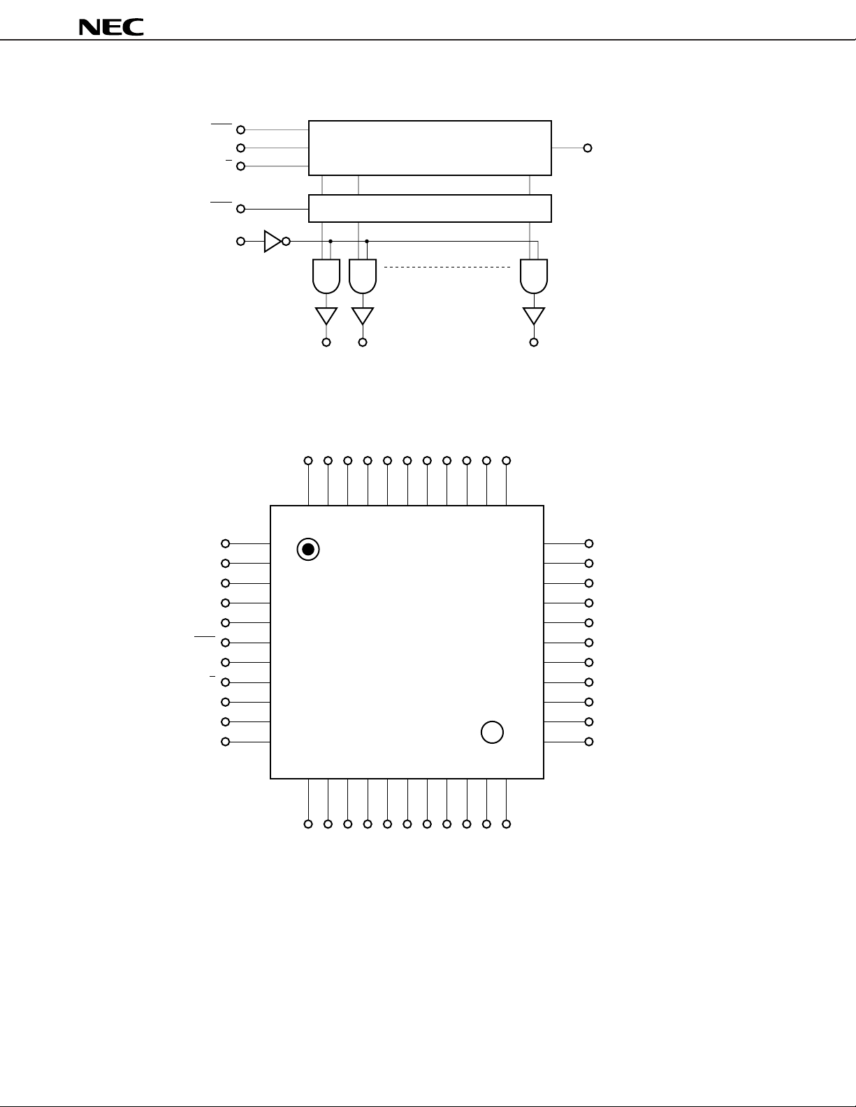
BLOCK DIAGRAM
CLK
R/L
µ
PD16326A
A
32-bit bidirectional shift registers
B
STB
BLK
PIN CONFIGURATION (Top View)
V
DD2
V
SS2
BLK
STB
CLK
V
SS1
R/L
V
DD1
SS2
V
A
B
1
2
3
4
5
6
7
8
9
10
11
32-bit latch
1
O
O
O1O2O3O4O5O6O7O8O9O10O
2
11
4443424140393837363534
O
33
32
31
30
29
28
27
26
25
24
23
32
O
12
O
13
O
14
O
15
O
16
O
17
O
18
O
19
O
20
O
21
O
22
1213141516171819202122
DD2
O32O31O30O29O28O27O26O25O24O
V
23
Remark Be sure to enter the power to VDD1, logic signal, and VDD2, in that order, and turn off the power in the reverse
order.
2
Page 3
µ
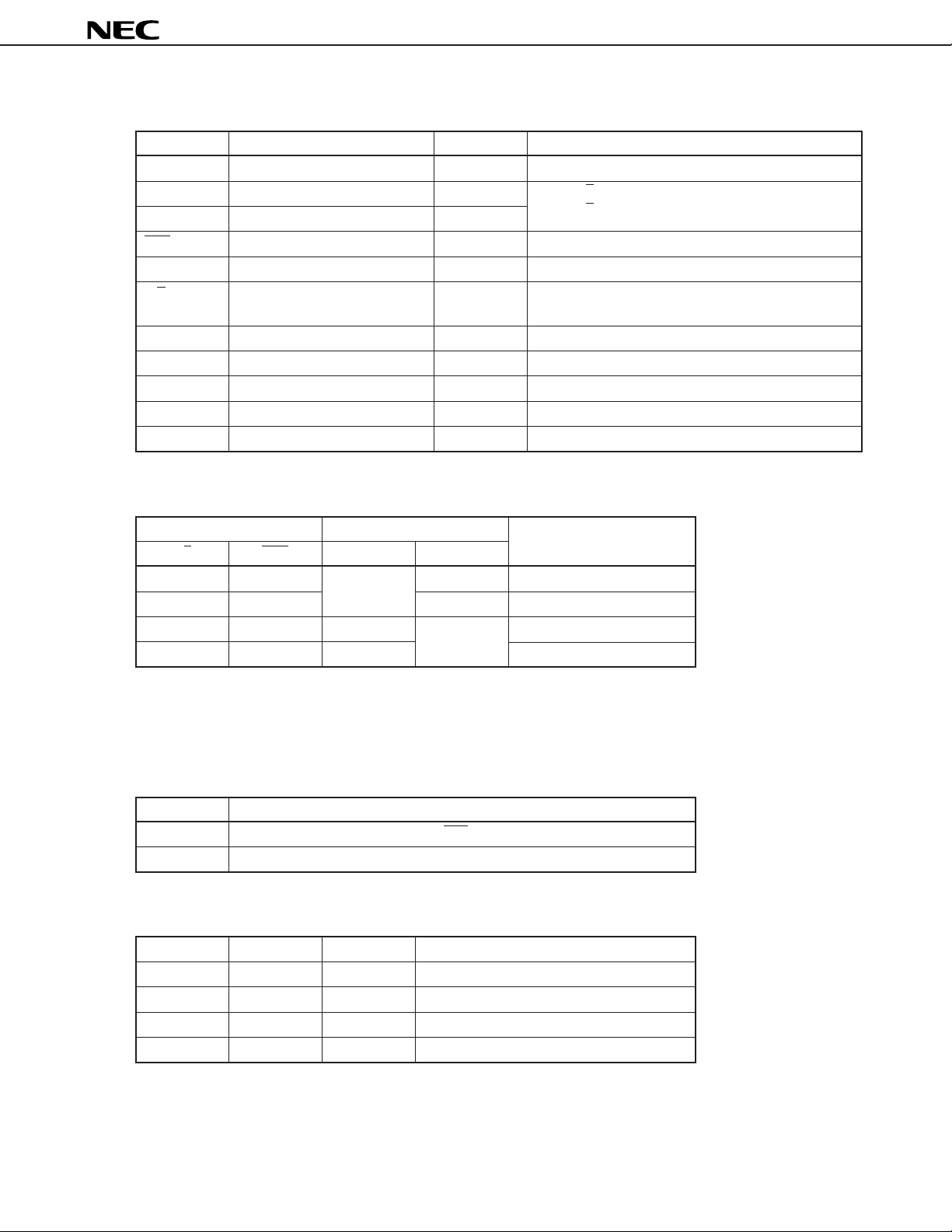
PIN DESCRIPTION
Pin Symbol Pin Name Pin Number Description
STB Latch strobe input 5 H: Data through L: Data retention
A RIGHT data input 3 When R/L = H, A: Input B: Output
B LEFT data input 10
CLK Clock input 6 Shift is executed on a fall.
BLK Blanking input 4 H: O1 to O32: ALL “L”
R/L Shift control input 8 H: Right shift mode A → O1 ... O32 → B
O1 to O32 High breakdown voltage output 13 - 44 130 V, 20 mA MAX
VDD1 Logic block power supply 9 5 V ±10 %
VDD2 Driver block power supply 1, 12 30 to 130 V
VSS1 Logic ground 5 Connected to system GND
VSS2 Driver ground 2, 11 Connected to system GND
TRUTH TABLE 1 (SHIFT REGISTER BLOCK)
When R/L = L, A: Output B: Input
L: Left shift mode B → O32 ... O1 → A
PD16326A
Input Output
R/L CLK A B
H ↓ Input Output
H H or L Output Retained
L ↓ Output
L H or L Output Retained
Note 2
Note 1
Input Execution of left shift
Shift Register
Execution of right shift
Notes 1. On a clock fall, the data items of S31 are shifted to S32, and output from B.
2. On a clock fall, the data items of S2 are shifted to S1, and output from A.
TRUTH TABLE 2 (LATCH BLOCK)
STB Operation
L Retains Sn data immediately before STB becomes L.
H Outputs shift register data.
TRUTH TABLE 3 (DRIVER BLOCK)
Note
Ln
××H L (all driver outputs: L)
× L L Outputs Sn data on STB fall.
LHLL
HHLH
STB BLK Driver output state
Note Ln: Latch output
Remark × = H or L, H = high level, L = Low level
3
Page 4
ABSOLUTE MAXIMUM RATINGS (TA = 25 ˚C, VSS = 0 V)
Item Symbol Rating Unit
Logic block supply voltage VDD1 –0.5 to +7.0 V
Driver block supply voltage VDD2 –0.5 to +150 V
Logic block input voltage VI –0.5 to VDD1 + 0.5 V
Driver block output current IO 20 mA
Package allowable power dissipation
Operating ambient temperature
Storage temperature Tstg –65 to +150 ˚C
PD 800
TA –40 to +85 ˚C
Note
mW
Note When TA ≥ 25 °C, load should be alleviated at a rate of –8.0 mW/°C. (Tj = 125 °C (MAX.))
RECOMMENDED OPERATING RANGE (TA = – 40 to +85 ˚C, VSS = 0 V)
Item Symbol MIN. TYP. MAX. Unit
Logic block supply voltage VDD1 4.5 5.0 5.5 V
Driver block supply voltage VDD2 30 130 V
Input voltage high VIH 0.7·VDD1 VDD1 V
Input voltage low VIL 0 0.2·VDD1 V
Driver output current IOH –10 mA
IOL +2.5 mA
µ
PD16326A
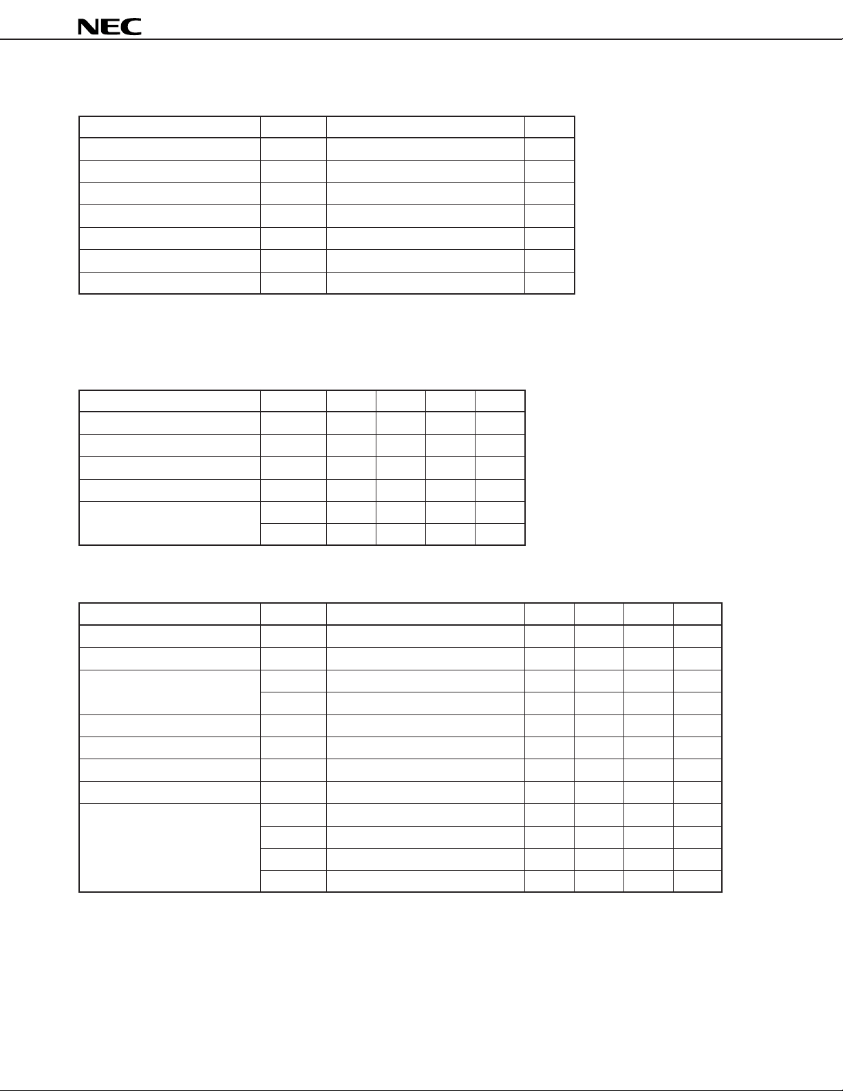
ELECTRICAL SPECIFICATIONS (TA = 25 ˚C, VDD1 = 4.5 to 5.5 V, VDD2 = 130 V, VSS = 0 V)
Item Symbol Condition MIN. TYP. MAX. Unit
Output voltage high VOH1 Logic, IOH = –1.0 mA 0.9·VDD1 VDD1 V
Output voltage low VOL1 Logic, IOL = 1.0 mA 0 0.1·VDD1 V
Output voltage high VOH21 O1 to O40, IOH = –0.5 mA 126 V
VOH22 O1 to O40, IOH = –5.0 mA 120 V
Output voltage low VOL2 O1 to O40, IOL = 0.5 mA 2.5 V
Input leakage current IIL VI = VDD1 or VSS1 ±1.0
Input voltage high VIH 0.7·VDD1 VDD1 V
Input voltage low VIL 0 0.2·VDD1 V
Static consumption current IDD1 Logic, TA = –40 to +85 ˚C 1 000
IDD1 Logic, TA = 25 ˚C 100
IDD2 Driver, TA = –40 to +85 ˚C 1 000
IDD2 Driver, TA = 25 ˚C 100
µ
A
µ
A
µ
A
µ
A
µ
A
4
Page 5

µ
PD16326A
SWITCHING CHARACTERISTICS (TA = 25 ˚C, VDD1 = 5.0 V, VDD2 = 130 V, VSS = 0 V, logic CL =
15 pF, driver CL = 50 pF, driver RL = 220 kΩ, tr = tf = 10 ns)
Item Symbol Condition MIN. TYP. MAX. Unit
Transmission delay time tPHL1 CLK ↓→ A/B 110 ns
tPLH1 110 ns
tPHL2 BLK ↓→ O1 to O32 300 ns
tPLH2 300 ns
Fall time tTHL O1 to O32 600 ns
Rise time tTLH O1 to O32 500 ns
Maximum clock frequency fmax With cascading, Duty = 50 % 8.0 MHz
Input capacitance CI 15 pF
TIMING REQUIREMENTS (TA = –40 to +85 ˚C, VDD1 = 4.5 to 5.5 V, VSS = 0 V, tr = tf = 10 ns)
Item Symbol Condition MIN. TYP. MAX. Unit
Clock pulse width PWCLK 40 ns
Strobe pulse width PWSTB 80 ns
Blank pulse width PWBLK 1 500 ns
Data setup time tsetup 15 ns
Data hold time thold 30 ns
Clock-strobe time tCLK-STB CLK ↓→ STB ↑ 45 ns
Strobe-clock time tSTB-CLK STB ↓→ CLK ↓ 45 ns
Strobe-blank time tSTB-BLK STB ↑→ BLK ↓ 80 ns
5
Page 6

SWITCHING CHARACTERISTIC WAVEFORM (R/L = H)
1/fmax.
PWCLK (L) PWCLK (H)
CLK
tsetup thold
50 % 50 % 50 %
µ
PD16326A
VDD1
VSS
A/B
(Input)
B/A
(Output)
STB
BLK
50 % 50 %
tPHL1
50 %
tCLK-STB tSTB-CLK
tSTB-BLK
PWSTB
PWBLK
50 %
VDD1
V
SS
tPLH 1
VOH1
50 %
V
OL1
VDD1
50 %50 %
V
SS
VDD1
50 %
V
SS
On
tPLH2 tTLH
90 %
10 %
tPHL2 tTHL
90 %
10 %
VOH2
VOL2
6
Page 7

PACKAGE DRAWINGS
44 PIN PLASTIC QFP (Unit: mm)
A
B
µ
PD16326A
34
33
23
22
C D
44
1
11
12
F
G
H
M
I
J
K
P
N
NOTE
Each lead centerline is located within 0.15 mm (0.006 inch) of
its true position (T.P.) at maximum material condition.
M
L
detail of lead end
S
13.6±0.4
10.0±0.2
10.0±0.2
+0.10
–0.05
R
Q
ITEM MILLIMETERS INCHES
A
B
C
D 13.6±0.4 0.535
F 1.0 0.039
G 1.0 0.039
H 0.35±0.10 0.014
I 0.15 0.006
J 0.8 (T.P.) 0.031 (T.P)
K 1.8±0.2 0.071
L 0.8±0.2 0.031
M 0.15 0.006
N 0.10 0.004
P 2.7 0.106
Q 0.1±0.1 0.004±0.004
R 5°±5° 5°±5°
S 3.0 MAX. 0.119 MAX.
+0.017
0.535
–0.016
+0.008
0.394
–0.009
+0.008
0.394
–0.009
+0.017
–0.016
+0.004
–0.005
+0.008
–0.009
+0.009
–0.008
+0.004
–0.003
P44GB-80-3B4-3
7
Page 8

µ
PD16326A
RECOMMENDED SOLDERING CONDITIONS
This product should be soldered and mounted under the conditions recommended below.
For soldering methods and conditions other than those recommended, please contact your NEC sales representative.
SURFACE MOUNT TYPE
For details of recommended soldering conditions, refer to the information document “Semiconductor Device
Mounting Technology Manual” (C10535E).
µ
PD16326GB-3B4
Soldering Method Soldering Conditions
Infrared reflow Package peak temperature: 235 ˚C, Duration: 30 sec. MAX.
(at 210 ˚C or above), Number of times: Twice, Time limit: None
VPS Package peak temperature: 215 ˚C, Duration: 40 sec. MAX.
(at 200 ˚C or above), Number of times: Twice, Time limit: None
Wave soldering Solder bath temperature: 260 ˚C MAX., Duration: 10 sec. MAX.,
Number of times: Once, Time limit: None
Pin partial heating Pin partial temperature: 300 ˚C MAX., Duration: 10 sec. MAX.,
Time limit: None
Note
Note
Note
Note
Recommended
Condition Symbol
IR35-00-2
VP15-00-2
WS60-00-1
Note For the storage period after dry-pack decapsulation, storage conditions are max. 25 ˚C, 65 % RH.
Caution Use of more than one soldering method should be avoided (except in the case of pin partial
heating).
REFERENCES
NEC Semiconductor Device Reliability/Quality Control System (IEI-1212)
Quality Grade on NEC Semiconductor Devices (C11531E)
8
Page 9

[MEMO]
µ
PD16326A
9
Page 10

[MEMO]
µ
PD16326A
10
Page 11

[MEMO]
µ
PD16326A
11
Page 12

µ
PD16326A
No part of this document may be copied or reproduced in any form or by any means without the prior written
consent of NEC Corporation. NEC Corporation assumes no responsibility for any errors which may appear in
this document.
NEC Corporation does not assume any liability for infringement of patents, copyrights or other intellectual property
rights of third parties by or arising from use of a device described herein or any other liability arising from use
of such device. No license, either express, implied or otherwise, is granted under any patents, copyrights or other
intellectual property rights of NEC Corporation or others.
While NEC Corporation has been making continuous effort to enhance the reliability of its semiconductor devices,
the possibility of defects cannot be eliminated entirely. To minimize risks of damage or injury to persons or
property arising from a defect in an NEC semiconductor device, customers must incorporate sufficient safety
measures in its design, such as redundancy, fire-containment, and anti-failure features.
NEC devices are classified into the following three quality grades:
"Standard", "Special", and "Specific". The Specific quality grade applies only to devices developed based on a
customer designated "quality assurance program" for a specific application. The recommended applications of
a device depend on its quality grade, as indicated below. Customers must check the quality grade of each device
before using it in a particular application.
Standard: Computers, office equipment, communications equipment, test and measurement equipment,
audio and visual equipment, home electronic appliances, machine tools, personal electronic
equipment and industrial robots
Special: Transportation equipment (automobiles, trains, ships, etc.), traffic control systems, anti-disaster
systems, anti-crime systems, safety equipment and medical equipment (not specifically designed
for life support)
Specific: Aircrafts, aerospace equipment, submersible repeaters, nuclear reactor control systems, life
support systems or medical equipment for life support, etc.
The quality grade of NEC devices is "Standard" unless otherwise specified in NEC's Data Sheets or Data Books.
If customers intend to use NEC devices for applications other than those specified for Standard quality grade,
they should contact an NEC sales representative in advance.
Anti-radioactive design is not implemented in this product.
M4 96.5
2
 Loading...