

Page 1
DATA SHEET
MOS INTEGRATED CIRCUIT
PD16312
1/4- to 1/11-DUTY FIPTM (VFD) CONTROLLER/DRIVER
The
PD16312 is a FIP (fluorescent Indicator Panel, or Vacuum Fluorescent Display) controller/driver that is
driven on a 1/4- to 1/11 duty factor. It consists of 11 segment output lines, 6 grid output lines, 5 segment/grid output
drive lines, a display memory, a control circuit, and a key scan circuit. Serial data is input to the PD16312 through a
three-line serial interface. This FIP controller/driver is ideal as a peripheral device for a single-chip microcomputer.
FEATURES
•Multiple display modes (11-segment & 11-digit to 16-segment & 4-digit)
•Key scanning (6 4 matrix)
•Dimming circuit (eight steps)
•High-voltage output (VDD 35 V max).
•LED ports (4 chs., 20 mA max).
•General-purpose input port (4 bits)
•No external resistors necessary for driver outputs (P-ch open-drain + pull-down resistor output)
•Serial interface (CLK, STB, DIN, D
OUT
)
ORDERING INFORMATION
Part Number Package
PD16312GB-3B4 44-pin plastic QFP ( 10)
Document No. IC-3307 (1st edition)
Date Published March 1997 P
Printed in Japan
1993©
Page 2
BLOCK DIAGRAM
PD16312
D
CLK
STB
V
DD
Key
to
Key
SW
to
SW
D
OUT
Command decoder
IN
Serial I/F
Display memeory
16 bits × 11 words
Dimming circuit
16-bit
16 11
output
latch
Segment
driver
Seg
Seg
1
11
5
R
OSC
Timing generator key scan
Key data memory (4 × 6)
11-bit
shift
Data
selector
5
5
Multip lexed
register
V
EE
(−30 V)
Grid
driver
1
4
4
1
4
4-bit
latch
4
4-bit latch
LED
1
LED
4
11 6
V
V
DD
(+5 V)
(0 V)
SS
Seg12/Grid
diver
Seg16/Grid
Grid
Grid
11
7
1
6
Key data memory (4 × 6)
2
Page 3
PIN CONFIGURATION (Top View)
SS43
OSC44
V
142
LED
241
LED
340
LED
439
LED
DD38
V
137
Grid
236
Grid
335
Grid
434
Grid
PD16312
SW1 1
2 2
SW
3 3
SW
4 4
SW
OUT 5
D
IN 6
D
SS 7
V
CLK 8
STB 9
1 10
KEY
2 11
KEY
KEY3 12
4 13
KEY
DD 14
V
1/KS1 15
Seg
2/KS2 16
Seg
3/KS3 17
Seg
4/KS4 18
Seg
5/KS5 19
Seg
6/KS6 20
Seg
7 21
Seg
8 22
Seg
Grid533
Grid
Seg
Seg
Seg
Seg
EE27
V
Seg
Seg
Seg
Seg
632
16/Grid731
15/Grid830
14/Grid929
13/Grid1028
12/Grid1126
1125
1024
923
Use all power pins.
3
Page 4
PD16312
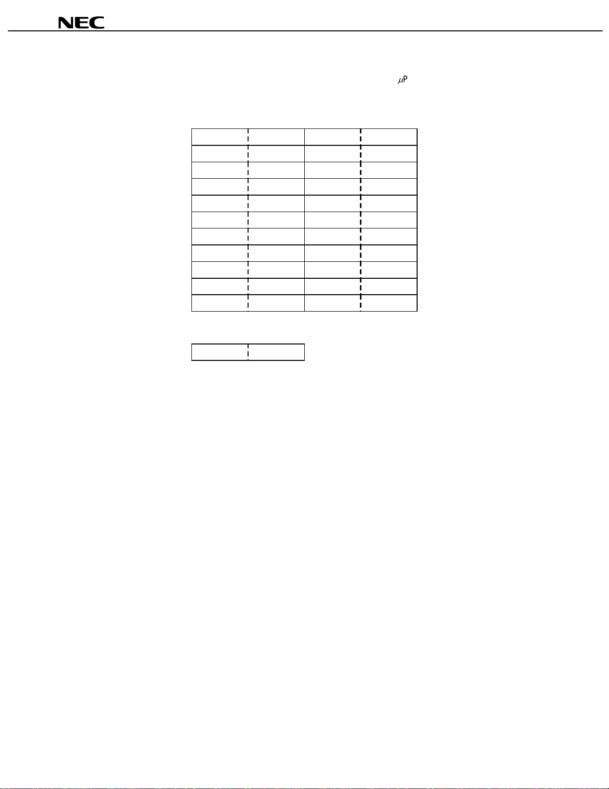
Pin Function
Symbol Pin Name Pin No Description
IN
D
OUT
D
STB Strobe 9 Initializes serial interface at the rising or falling edge of the
CLK Clock input 8 Reads serial data at the rising edge, and outputs data at the
OSC Oscillator pin 44 Connect resistor to this pin to determine the oscillation frequency
Seg1/KS1 to
6
6
/KS
Seg
Seg7 to Seg
Grid1 to Grid
11
6
Seg12/Grid11 to
16
7
/Grid
Seg
LED1 to LED
KEY1 to KEY
SW1 to SW
DD
V
SS
V
EE
V
4
4
4
Data input 6 Input serial data at rising edge of shift clock, starting from the low
order bit.
Data output 5 Output serial data at the falling edge of the shift clock, starting
from low order bit. This is N-ch open-drain output pin.
PD16312. It then waits for reception of a command. Data input
after STB has fallen is processed as a command. While
command data is processed, current processing is stopped, and
the serial interface is initialized. While STB is high, CLK is
ignored.
falling edge.
to this pin.
High-voltage output 15 to 20 Segment output pins (Dual function as key source)
High-voltage output
21 to 25 Segment output pins
(segment)
High-voltage output (grid) 37 to 32 Grid output pins
High-voltage output
26, 28 to 31
These pins are selectable for segment or grid driving.
(segment/grid)
LED output 42 to 39 CMOS output. +20 mA max.
Key data input 10 to 13 Data input to these pins is latched at the end of the display cycle.
Switch input 1 to 4 These pins constitute a 4-bit general-purpose input port.
Logic power 14, 38 5 V 10 %
Logic ground 7, 43 Connect this pin to system GND.
Pull-down level 27 VDD 35 V max.
4
Page 5
PD16312
Display RAM Address and Display Mode
The display RAM stores the data transmitted from an external device to the PD16312 through the serial interface,
and is assigned addresses as follows, in 8 bits unit:
Seg
0
b
1
00H
02H
04H
06H
08H
0AH
0CH
0EH
10H
12H
14H
xxH
L
L
L
L
L
L
L
L
L
L
L
L
Seg
b3b
4
00H
02H
04H
06H
08H
0AH
0CH
0EH
10H
12H
14H
4
xxH
Lower 4 bits Higher 4 bits
8
Seg
U
U
U
U
U
U
U
U
U
U
U
U
01H
03H
05H
07H
09H
0BH
0DH
0FH
11H
13H
15H
7
b
Seg
L
L
L
L
L
L
L
L
L
L
L
12
01H
03H
05H
07H
09H
0BH
0DH
0FH
11H
13H
15H
U
U
U
U
U
U
U
U
U
U
U
Seg
16
1
DIG
2
DIG
3
DIG
4
DIG
5
DIG
6
DIG
7
DIG
8
DIG
9
DIG
10
DIG
11
DIG
5
Page 6
PD16312
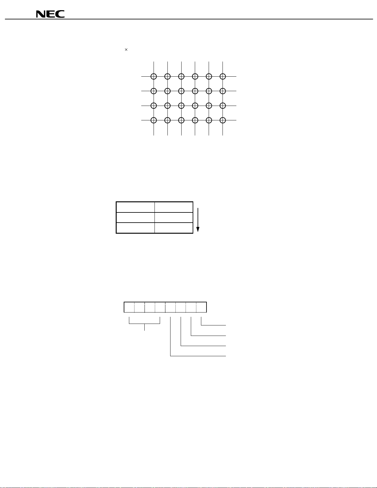
Key Matrix and Key-Input Data Storage RAM
The key matrix is made up of a 6 4 matrix, as shown below.
KEY
1
KEY
2
KEY
3
KEY
4
1
2
3
4
5
6
/KS
/KS
/KS
/KS
/KS
1
Seg
2
Seg
3
Seg
4
Seg
5
Seg
/KS
6
Seg
The data of each key is stored as illustrated below, and is read with the read command, starting from the least
significant bit.
KEY1…KEY4KEY1…KEY
4
Seg1/KS
Seg3/KS
Seg5/KS
1
3
5
Seg2/KS
Seg4/KS
Seg6/KS
2
4
6
Reading sequence
b0------------b3 b4------------b7
LED Port
Data is written to the LED port with the write command, starting from the least port’s least significant bit. When a
bit of this port is 0, the corresponding LED lights; when the bit is 1, the LED truns off. The data of bits 5 through 8 are
ignored.
MSB
−−−−b3 b2 b1 b0
Don't care
LSB
LED1
LED2
LED3
LED4
On power application, all LEDs are unlit.
6
Page 7

PD16312
SW Data
SW data is read with the read command, starting from the least significant bit. Bits 5 through 8 of the SW data are
0.
MSB
0 0 0 0 b3 b2 b1 b0
LSB
SW1
SW2
SW3
SW4
Commands
Commands set the display mode and status of the FIP driver.
The first 1 byte input to the PD16312 through the D
IN
pin after the STB pin has fallen is regarded as a command.
If STB is set high while commands/data are transmitted, serial communication is initialized, and the
commands/data being transmitted are invalid (however, the commands/data previously transmitted remain valid).
(1) Display mode setting commands
These commands initialize the PD16312 and select the number of segments and the number of grids (1/4 to
1/11 duty, 11 segments to 16 segments).
When these commands are executed, the display is forcibly turned off, and key scanning is also stopped. To
resume display, the display command “ON” must be executed. If the same mode is selected, however, nothing
happens.
MSB
00−−−b2 b1 b0
Irrelevant
LSB
Display mode settings
000
001
010
011
100
101
110
111
On power application, the 11-digit, 11-segment mode is selected.
: 4 digits, 16 segments
: 5 digits, 16 segments
: 6 digits, 16 segments
: 7 digits, 15 segments
: 8 digits, 14 segments
: 9 digits, 13 segments
: 10 digits, 12 segments
: 11 digits, 11 segments
7
Page 8

(2) Data setting commands
These commands set data write and data read modes.
PD16312
MSB
01−−b3 b2 b1 b0
Irrelevant
LSB
Data write and read mode settings
00
: Write data to display memory
01
: Write data to LED port
10
: Read key data
11
: Read SW data
Address increment mode settings (display memory)
01: Increments address after data has been written
: Fixes address.
Test mode settings
01: Normal operation
: Test mode
On power application, the normal operation and address increment modes are set.
(3) Address setting commands
These commands set an address of the display memory.
MSB
11−b4 b3 b2 b1 b0
LSB
Address (00H - 15H)
If address 16H or higher is set, data is ignored, until a valid address is set.
On power application, the address is set to 00H.
8
Page 9

(4) Display control commands
PD16312
MSB
10−−b3 b2 b1 b0
Irrelevant
LSB
Dimming quantity settings
000
: Set pulse width to 1/16.
001
: Set pulse width to 2/16.
010
: Set pulse width to 4/16.
011
: Set pulse width to 10/16.
100
: Set pulse width to 11/16.
101
: Set pulse width to 12/16.
110
: Set pulse width to 13/16.
111
: Set pulse width to 14/16.
Turns on/off display.
01: Display off (key scan continues
: Display on
On power application, the 1/16 pulse width is set and the display is turned off.
On power application, key scanning is stopped.
Note
Note
)
9
Page 10

Key Scanning and Display Timing
T
DISP
= 500 s
µ
Key scan data
PD16312
SEG output DIG1
G
1
DIG2 DIG3
DIGn 1 5 6342
1/16
T
G
2
G
3
G
n
DISP
1 frame = T
DISP
× (n + 1)
One cycle of key scanning consists of one frame, and data in a 6 4 matrix is stored in RAM.
DIG1
10
Page 11

Serial Communication Format
Reception (command/data write)
STB
PD16312
If data continues
D
CLK
IN
b0 b1 b2 b6 b7
123 78
Transmission (data read)
STB
D
IN
CLK 123456 12345678
D
OUT
Because the D
b0 b1 b2 b3 b4 b5
A data read command is set. Data is read.
OUT
pin is an N-ch, open-drain output pin, be sure to connect an external pull-up resistor to this pin
b6 b7
(1 k to 10 k).
When data is read, a wait time t
Note
WAIT
of 1 s is necessary since the rising of the eighth clock that has set the
command, until the falling of the first clock that has read the data.
t
WAIT
Note
b0 b1 b2 b3 b4 b5
11
Page 12

PD16312
ABSOLUTE MAXIMUM RATINGS (Ta = 25
C, VSS = 0 V)
PARAMETER SYMBOL RATINGS UNIT
Logic Supply Voltage V
Driver Supply Voltage V
Logic Input Voltage V
FIP Driver Output Voltage V
LED Driver Output Current I
FIP Driver Output Current I
Power Dissipation P
Operating Ambient temperature T
Storage Temperature T
Derate at 6.4 mW/C at T
Note
DD
EE
I1
O2
O1
O2
D
opt
stg
a
= 25 C or higher.
VDD +0.5 to VDD 40 V
VEE 0.5 to VDD +0.5 V
RECOMMENDED OPERATING RANGE (Ta =
PARAMETER SYMBOL MIN. TYP. MAX. UNIT TEST CONDITIONS
0.5 to +7.0 V
DD
0.5 to V
+0.5 V
+25 mA
40 (grid)
15 (segment)
Note
800
40 to +85
65 to +150
20 to 70
C, VSS = 0 V)
mA
mW
C
C
Logic Supply Voltage V
High-Level Input Voltage V
Low-Level Input Voltage V
Driver Supply Votlage V
Maximum power consumption P
DD
IH
IL
EE
MAX
. = FIP driver dissipation + RL dissipation + LED driver dissipation + dynamic
4.5 5 5.5 V
DD
0.7 V
0 0.3 V
0V
DD
V
DD
DD
35 V
V
V
power consumption
Where segment current = 3 mA, grid current = 15 mA, and LED current = 20 mA,
FIP driver dissipation = number of segments 6 + number of grids/(number of grids + 1) 30 (mW)
RL dissipation = (VDD VEE)2/50 (number of segments + 1) (mW)
LED driver dissipation = number of LEDs 20 (mW)
Dynamic power consumption = VDD 5 (mW)
Example
Where VEE = 25 V, VDD = 5 V, and in 16-segment and 6-digit modes,
FIP driver dissipation = 16 6 + 6/7 30 = 122
RL dissipation = 302/50 17 = 306
LED driver dissipation = 4 20 = 80
Dynamic power consumption = 5 5 = 25
Total 553 mW
12
Page 13

PD16312
ELECTRICAL CHARACTERISTICS (Ta =
PARAMETER SYMBOL MIN. TYP. MAX. UNIT TEST CONDITIONS
High-Level Output Voltage V
Low-Level Output Voltage V
Low-Level Output Voltage V
High-Level Output Current I
High-Level Output Current I
Driver Leakage Current I
Output Pull-Down Resistor R
Input Current I
High-Level Input Voltage V
Low-Level Input Voltage V
Hysteresis Voltage V
Dynamic Current Consumption I
OH1
OL1
OL2
OH21
OH22
OLEAK
L
I
IH
IL
H
DDdyn
SWITCHING CHARACTERISTICS (Ta =
20 to +70
DD
0.9 V
3mAV
15 mA V
50 100 150 K
DD
0.7 V
C, VDD = 4.5 to 5.5 V, VSS = 0 V, VEE = VDD
1
4
V LED
1 V LED1 LED4, I
0.4 V D
OUT
, I
O
= VDD 2 V, Seg1 to Seg
O
= VDD 2 V, Grid1 to Grid
Seg12/ Grid11 to Seg
10
1
AV
Driver output
AV
O
= VDD 35 V, driver off
I
= VDD or V
V
DD
0.3 V
V
LED
OL2
= 4 mA
OH1
, I
OL1
SS
= 1 mA
= 20 mA
16/
0.35 V CLK, DIN, STB
5 mA Under no load, display off
20 to +70
C, VDD = 4.5 to 5.5 V, VEE =
30 V)
Grid
35 V)
11
6
7
PARAMETER SYMBOL MIN. TYP. MAX. UNIT TEST CONDITIONS
Oscillation Frequency t
Propagation Delay Time t
Rise Time t
Fall Time t
Maximum Clock Frequency f
Input Capacitance C
TIMING CONDITIONS (Ta =
20 to 70
PARAMETER SYMBOL MIN. TYP. MAX. UNIT TEST CONDITIONS
Clock Pule Width PW
Strobe Pulse Width PW
Data Setup Time t
Data Hold Time t
Clock-Strobe Time t
Wait Time t
OSC
PLZ
PZL
t
TZH1
TZH2
t
THZ
max.
I
CLK
STB
SETUP
HOLD
CLK-STB
WAIT
350 500 650 kHz R = 51 k
300 ns CLK D
100 ns CL = 15 pF, RL = 10 k
2
0.5
120
sCL = 300 pF Seg1 to Seg
s Grid1 to Grid6,
sCL = 300 pF, Segn, Grid
1 MHz Duty = 50 %
15 pF
C, VDD = 4.5 to 5.5 V)
400 ns
1
100 ns
100 ns
1
1
s
s CLK STB
s
OUT
CLK CLK
Seg
Seg
Note
12
/Grid11 to
16
/Grid
n
11
7
Refer to page 11.
Note
13
Page 14

Switching Characteristic Waveforms
f
OSC
OSC
50 %
STB
PD16312
PWSTB
CLK
DIN
DOUT
Sn/Gn
PWCLK PWCLK
tSETUP tHOLD
90 %
10 %
tCLK-STB
tPZL
tTHZ tTZH
tPLZ
14
Page 15

Applications
Updating display memory by incrementing address
STB
CLK
D
IN
Command 2 Command 3 Data 1 Data n Command 4Command 1
Command 1:sets display mode
Command 2:sets data
Command 3:sets address
Data 1 to n: transfers display data (22 bytes max.)
Command 4:controls diplay
PD16312
Updating specific address
STB
CLK
D
IN
Command 1:sets data
Command 2:sets address
Data: display data
Command 2 Data Command 2 DataCommand 1
15
Page 16

PD16312
RECOMMENDED SOLDERING CONDITIONS
The following conditions (see table below) must be met when soldering this product. Please consult with our sales
offices in cae other soldering process is used, or in case soldering is done under different conditions.
PC16312GB-3B4
Soldering process Soldering conditions Symbol
Infrared ray reflow Peak package’s surface temperature: 235 C or below,
Reflow time: 30 seconds or below (210 C or higher),
Number of reflow process: 2, Exposure limit*: None
VPS Peak package’s surface temperature: 215 C or below,
Reflow time: 40 seconds or below (200 C or higher),
Number of reflow process: 2, Exposure limit*: None
Wave soldering Solder temperature: 260 C or below,
Flow time: 10 seconds or below
Number of flow process: 1, Exposure limit*: None
Partial heating method Terminal temperature: 300 C or below,
Flow time 10 seconds or below,
Exposure limit*: None
Exposure limit before soldering after dry-pack package is opened.
*
Storage conditions: 25 C and relative humidity at 65 % or less.
Do not apply more than a single process at once, except for “Partial heating method”.
Note
IR35-00-2
VP15-00-2
WS60-00-1
16
Page 17

44 PIN PLASTIC QFP ( 10)
A
B
PPPP
PD16312
34
33
23
22
C D
44
1
11
12
F
G
H
M
I
J
K
P
N
NOTE
Each lead centerline is located within 0.15 mm (0.006 inch) of
its true position (T.P.) at maximum material condition.
M
L
detail of lead end
S
13.6±0.4
10.0±0.2
10.0±0.2
+0.10
–0.05
R
Q
ITEM MILLIMETERS INCHES
A
B
C
D 13.6±0.4 0.535
F 1.0 0.039
G 1.0 0.039
H 0.35±0.10 0.014
I 0.15 0.006
J 0.8 (T.P.) 0.031 (T.P)
K 1.8±0.2 0.071
L 0.8±0.2 0.031
M 0.15 0.006
N 0.10 0.004
P 2.7 0.106
Q 0.1±0.1 0.004±0.004
R 5˚±5˚ 5˚±5˚
S 3.0 MAX. 0.119 MAX.
+0.017
0.535
–0.016
+0.008
0.394
–0.009
+0.008
0.394
–0.009
+0.017
–0.016
+0.004
–0.005
+0.008
–0.009
+0.009
–0.008
+0.004
–0.003
P44GB-80-3B4-3
17
Page 18

[MEMO]
PD16312
18
Page 19

[MEMO]
PD16312
19
Page 20

PD16312
FIPTM is a trademark of NEC Corporation.
No part of this document may be copied or reproduced in any form or by any means without the prior written
consent of NEC Corporation. NEC Corporation assumes no responsibility for any errors which may appear in this
document.
NEC Corporation does not assume any liability for infringement of patents, copyrights or other intellectual
property rights of third parties by or arising from use of a device described herein or any other liability arising
from use of such device. No license, either express, implied or otherwise, is granted under any patents,
copyrights or other intellectual property rights of NEC Corporation or others.
While NEC Corporation has been making continuous effort to enhance the reliability of its semiconductor devices,
the possibility of defects cannot be eliminated entirely. To minimize risks of damage or injury to persons or
property arising from a defect in an NEC semiconductor device, customers must incorporate sufficient safety
measures in its design, such as redundancy, fire-containment, and anti-failure features.
NEC devices are classified into the following three quality grades:
"Standard", "Special", and "Specific". The Specific quality grade applies only to devices developed based on
a customer designated "quality assurance program" for a specific application. The recommended applications
of a device depend on its quality grade, as indicated below. Customers must check the quality grade of each
device before using it in a particular application.
Standard: Computers, office equipment, communications equipment, test and measurement equipment,
audio and visual equipment, home electronic appliances, machine tools, personal electronic
equipment and industrial robots
Special: Transportation equipment (automobiles, trains, ships, etc.), traffic control systems, anti-disaster
systems, anti-crime systems, safety equipment and medical equipment (not specifically designed
for life support)
Specific: Aircrafts, aerospace equipment, submersible repeaters, nuclear reactor control systems, life
support systems or medical equipment for life support, etc.
The quality grade of NEC devices is "Standard" unless otherwise specified in NEC's Data Sheets or Data Books.
If customers intend to use NEC devices for applications other than those specified for Standard quality grade,
they should contact an NEC sales representative in advance.
Anti-radioactive design is not implemented in this product.
M4 96. 5
 Loading...