

Page 1
DATA SHEET
BIPOLAR ANALOG INTEGRATED CI RCUIT
µ
µ
PC8163TB
µµ
SILICON MMIC 2.0 GHz FREQUENCY UP-CONVERTER
FOR CELLULAR TELEPHONE
DESCRIPTION
The µPC8163TB is a silicon monolithic integrated circuit designed as frequency up-converter for cellular telephone
transmitter stage. The µPC8163TB has improved intermodulation performance and smaller package.
The µPC8163TB is manufactured using NEC’s 20 GHz fT NESATTMlll silicon bipolar process. This process uses
silicon nitride passivation film and gold electrodes. These materials can protect chip surface from external pollution
and prevent corrosion/migration. Thus, this IC has excellent performance, uniformity and reliability.
FEATURES
• Recommended operating frequency : f
• Supply voltage : V
• High-density surface mounting : 6-pin super minimold package
• Higher IP
• Minimized carrier leakage : Due to double balanced mixer
3
RFout
= 0.8 GHz to 2.0 GHz, f
CC
= 2.7 to 3.3 V
: OIP3 = +9.5 dBm @ f
RFout
IFin
= 50 MHz to 300 MHz
= 830 MHz
APPLICATIONS
• Digital cellular phones
ORDERING INFORMATION
Part Number Package Supplying Form
µ
PC8163TB-E3 6-pin super minimold
Remark
To order evaluation samples, please contact your local NEC sales office.
(Part number for sample order:
PC8163TB)
µ
Embossed tape 8 mm wide.
Pin 1, 2, 3 face to tape perf oration side.
Qty 3 kp/reel
The information in this document is subject to change without notice. Before using this document, please
confirm that this is the latest version.
Not all devices/types available in every country. Please check with local NEC representative for
availability and additional information.
Document No. P13636EJ2V0DS00 (2nd edition)
Date Published June 1999 N CP(K)
Printed in Japan
Caution Electro-static sensitive device
The mark shows major revised points.
1998, 1999©
Page 2
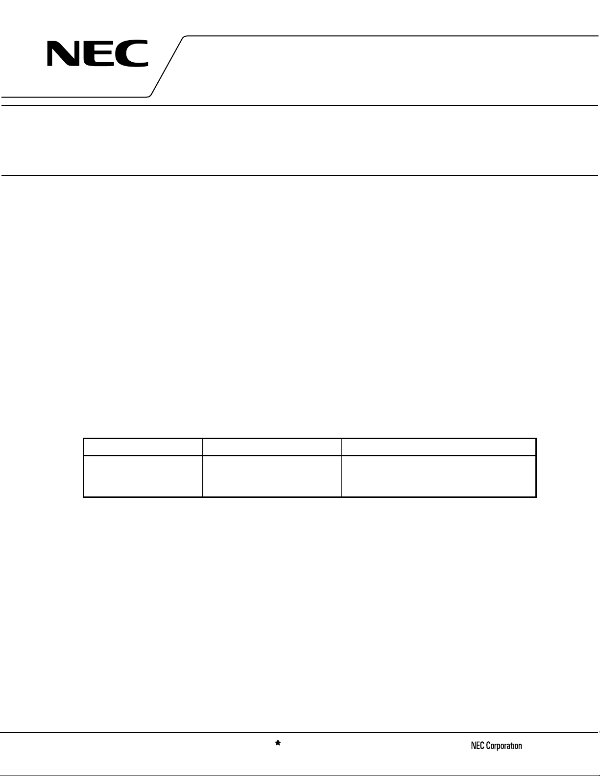
PIN CONNECTIONS
(Top View)
3
µµµµ
PC8163TB
(Bottom View)
4
4
3
Pin No. Pin Name
1 IFinput
2GND
2
1
C2Y
5
5
6
6
SERIES PRODUCTS (TA = +25°C, VCC = V
Type Part No. VCC (V)
3
High IP
Low Power ConsumptionµPC8109TB
Higher IP
3
PC8106TB
µ
PC8163TB
µ
RFout
= 3.0 V, ZL = ZS = 50
CC
I
(mA)
2.7 to
5.5
2.7 to
5.5
2.7 to
3.3
9 9 7 –2 –4 +5.5 +2.0
5 6 4 –5.5 –7.5 +1.5 –1.0
16.5 9 5.5 0.5 –2 +9.5 +6.0
CG1
(dB)
2
1
)
ΩΩΩΩ
CG2
(dB)
O(sat)
P
(dBm)
3 LOinput
4GND
5V
6 RFoutput
O(sat)
1
P
2
(dBm)
CC
OIP31
(dBm)
OIP32
(dBm)
Caution The above table lists the typical performance of each model. See ELECTRICAL CHARACTERISTICS for
the test conditions.
BLOCK DIAGRAM (FOR THE
PC8163TB)
µµµµ
LOinput
GND
IFinput
(Top View)
GND
V
CC
RFoutput
2
Data Sheet P13636EJ2V0DS00
Page 3
µµµµ
PC8163TB
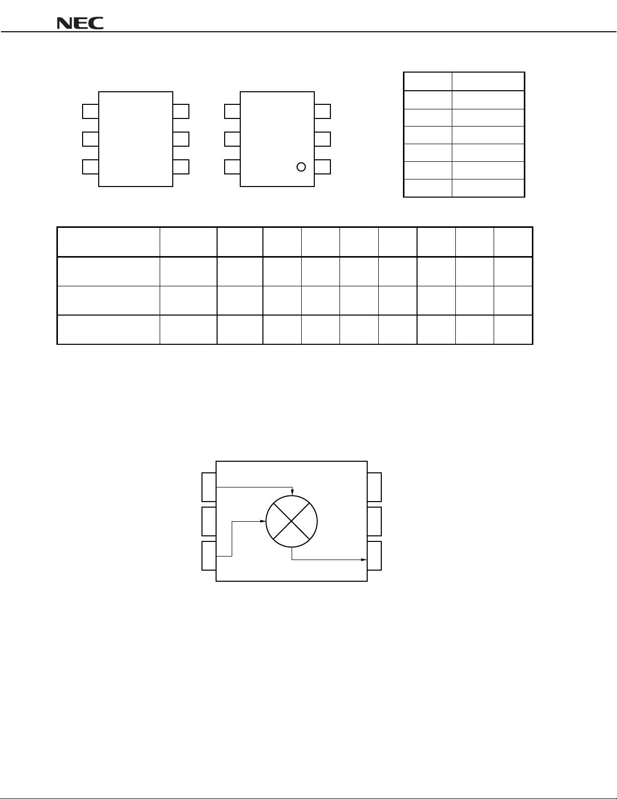
SYSTEM APPLICATION EXAMPLES (SCHEMATICS OF IC LOCATION IN THE SYSTEM)
RX
TX
SW
PA
VCO
µ
PC8163TB
÷N PLL
Phase
shifter
0˚
90˚
DEMO.
PLL
I
Q
I
Q
Data Sheet P13636EJ2V0DS00
3
Page 4
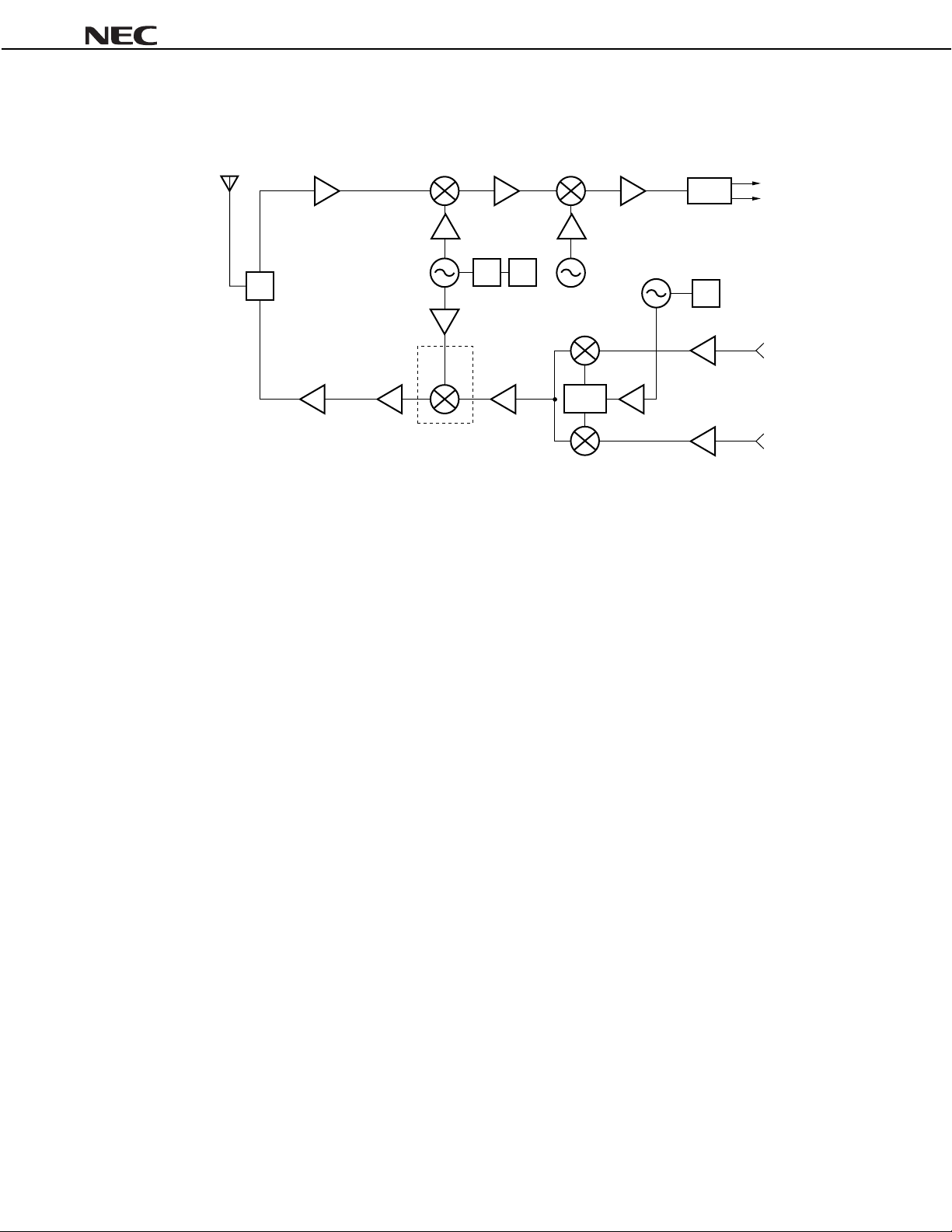
PIN EXPLANATION
µµµµ
PC8163TB
Pin
No.
1 IFinput
2
4
3 LOinput
5VCC2.7 to 3.3
6 RFoutput Same
Pin
Name
GND 0
Applied
Voltage
V
bias as
CC
V
through
external
inductor
Pin
Voltage
Note
V
1.2
2.1 Local input pin. Recommendable input level
This pin is IF input to doubl e bal anced mixer
(DBM). The input is designed as hi gh
impedance. The circuit contributes to
suppress spurious signal . Also this
symmetrical ci rcuit can keep specified
performance insensitive to process-condition
distribution. For above reason, double
balanced mixer is adopted.
GND pin. Ground pattern on the board
should be formed as wide as poss i bl e.
Track Length should be kept as short as
possible to minimiz e ground i m pedance.
is –10 to 0 dBm.
Supply voltage pin.
This pin is RF output from DB M . This pin is
designed as open collector. Due to the high
impedance output, this pi n should be
externally equipped with LC mat c hi ng circuit
to next stage.
Function and Explanation Equivalent Circuit
5
6
3
1
2
Each pin voltage is measured with V
Note
CC
= V
RFout
= 3.0 V.
4
Data Sheet P13636EJ2V0DS00
Page 5
ABSOLUTE MAXIMUM RATINGS
Parameter Symbol Test Conditions Rating Unit
µµµµ
PC8163TB
Supply Voltage V
Power Dissipation of Package P
Operating Ambient Temperature T
Storage Temperature T
Maximum Input Power P
CC
D
A
stg
in
RECOMMENDED OPERATING CONDITIONS
Parameter Symbol Test Conditions MIN. TYP. MAX. Unit
Supply Voltage V
Operating Ambient Temperature T
Local Input Level P
RF Output Frequency f
IF Input Frequency f
CC
A
LOin
RFout
IFin
ELECTRICAL CHARACTERISTICS
(TA = +25
C, VCC = V
°°°°
RFout
= 3.0 V, f
Parameter Symbol Conditions MIN. TYP. MAX. Unit
IFin
= 150 MHz, P
TA = +25°C, Pin 5 and 6 3.6 V
Mounted on double-sided copperclad 50 × 50 × 1.6
200 mW
mm epoxy glass PWB
A
= +85°C
T
40 to +85 °C
−
55 to +150 °C
−
+10 dB m
The same voltage should be applied
2.7 3.0 3.3 V
to pin 5 and 6
40 +25 +85 ° C
−
Zs = 50 Ω (without matching) –10 –5 0 dBm
With external matching c i rcuit 0.8 – 2.0 GHz
50 – 300 MHz
LOin
= –5 dBm)
Circuit Current I
Conversion Gain 1 CG1 f
Conversion Gain 2 CG2 f
Maximum RF Output Power 1 P
Maximum RF Output Power 2 P
CC
O(sat)
1f
O(sat)
2f
No Signal 11.5 16.5 23 mA
RFout
= 830 MHz, P
RFout
= 1.9 GHz, P
RFout
= 830 MHz, P
RFout
= 1.9 GHz, P
IFin
= –20 dBm 6 9 12 dB
IFin
= –20 dBm 2.5 5.5 8.5 dB
IFin
= 0 dBm –1.5 0.5 – dBm
IFin
= 0 dBm –4.5 –2 – dBm
OTHER CHARACTERISTICS, FOR REFERENCE PURPOSES ONLY
(TA = +25
C, VCC = V
°°°°
RFout
= 3.0 V, P
Parameter Symbol Conditions Data Unit
Point
Intercept Point
SSB Noise Figure SSB NF f
LOin
= –5 dBm)
IFin
IIP3 1f
IIP
OIP3 1f
OIP
f
1 = 150.0 MHz
IFin
f
3
2
3
2
2 = 150.4 MHz
IFin
f
1 = 150.0 MHz
IFin
f
2 = 150.4 MHz
RFout
= 830 MHz, f
IFin
= 150 MHz 12.5 dB
RFout
= 830 MHz 0.5Input Third Order Distortion Int ercept
RFout
= 1.9 GHz 0.5
f
RFout
= 830 MHz +9.5Output Third-Order Distortion
RFout
= 1.9 GHz +6.0
f
dBm
dBm
Data Sheet P13636EJ2V0DS00
5
Page 6

µµµµ
PC8163TB
V
50 Ω
CC
RFout
10 000
pF
= 830 MHz)
RF = 830 MHz matched
1 000 pF
10 nH
6
5
4
RFoutput
CC
V
GND
IFinput
GND
LOinput
100 pF1 pF1 000 pF
1
2
100 pF
3
TEST CIRCUIT 1 (f
Spectrum Analyzer
ILLUSTRATION OF TEST CIRCUIT 1 ASSEMBLED ON EVALUATION BOARD
IF
RF
1 000 pF
OUT
1 000 pF
1 pF
10 nH
1
10 nH
IN
100 pF
Signal Generator
50 Ω
Signal Generator
50 Ω
Loin
= –5 dBm
P
EVALUATION BOARD CHARACTERS
(1) 35
m thick double-sided copper clad 35 × 42 × 0.4 mm polyimide board
µ
(2) Back side: GND pattern
(3) Solder plated patterns
{
(4)
ATTENTION
: Through holes
{
Test circuit or print pattern in this sheet is for testing IC characteristics.
In the case of actual system application, external circuits including print pattern and matching circuit
constant of output port should be designed in accordance with IC’s S parameters and environmental
components.
PC8163TB
µ
10 000 pF
100 pF
LO
IN
6
Data Sheet P13636EJ2V0DS00
Page 7

µµµµ
PC8163TB
50 Ω
CC
V
RFout
10 000
pF
= 1.9 GHz)
RF = 1.9 GHz matched
1 000 pF
2.5 pF
100 nH
6
5
4
RFoutput
CC
V
GND
IFinput
GND
LOinput
100 pF Strip Line1 000 pF
1
2
100 pF
3
TEST CIRCUIT 2 (f
Spectrum Analyzer
ILLUSTRATION OF TEST CIRCUIT 2 ASSEMBLED ON EVALUATION BOARD
2 pF
IN
RFOUT
1 000 pF
1 000 pF
0.5 pF
100 nH
1
IF
100 pF
100 pF
Signal Generator
50 Ω
Signal Generator
50 Ω
Loin
= –5 dBm
P
EVALUATION BOARD CHARACTERS
(1) 35
m thick double-sided copper clad 35 × 42 × 0.4 mm polyimide board
µ
(2) Back side: GND pattern
(3) Solder plated patterns
{
(4)
: Through holes
{
PC8163TB
µ
10 000 pF
100 pF
LOIN
100 pF
Data Sheet P13636EJ2V0DS00
7
Page 8

µµµµ
PC8163TB
TYPICAL CHARACTERISTICS (TA = +25
CIRCUIT CURRENT vs. SUPPLY VOLTAGE
25
no signals
20
(mA)
CC
15
10
Circuit Current I
5
0
01234
CC
Supply Voltage V
(V) Operating Ambient Temperature TA (°C)
C, unless otherwise specified VCC = V
°°°°
S-PARAMETER FOR MATCHED RF OUTPUT (VCC = V
RFout
(mA)
CC
Circuit Current I
= 3.0 V)
30
no signals
25
20
15
10
5
0
–60 –40 –20 0 20 40 60 80 100
with TEST CIRCUITS 1 and 2
−−−−
RFout
)
CIRCUIT CURRENT vs. OPERATING
AMBIENT TEMPERATURE
(monitored at RF connector on board)
• RF output matched at 830 MHz • RF output matched at 1.9 GHz
−−−−
CH1
PRm
Cor
Del
Hld
START 100.000 000 MHz STOP 3 000.000 000 MHz
CH1
PRm
Cor
Del
Hld
1 U FS 1; 53.422 Ω Ω Ω ΩS
11
[hp]
MARKER1
830 MHz
S
11
log MAG 10 dB/ REF 0 dB 1;–17.331 dB
[hp]
MARKER1
830 MHz
1
–14.973 12.807 pF
830.000 000 MHz
1
830.000 000 MHz
CH1
PRm
Cor
Del
Smo
Hld
START 100.000 000 MHz STOP 3 000.000 000 MHz
CH1
PRm
Cor
Del
Smo
Hld
1 U FS 2; 53.846S
11
[hp]
MARKER2
1.9 GHz
S
11
log MAG 10 dB/ REF 0 dB 2;–24.741 dB
[hp]
MARKER2
1.9 GHz
1
–3.7441 22.373 pF
1 900.000 000 MHz
2
1 900.000 000 MHz
2
1;–.5113 dB
830 MHz
START 100.000 000 MHz STOP 3 000.000 000 MHz
8
START 100.000 000 MHz STOP 3 000.000 000 MHz
Data Sheet P13636EJ2V0DS00
Page 9

µµµµ
PC8163TB
S-PARAMETERS FOR EACH PORT (VCC = V
RFout
= 3.0 V)
LO port RF port (no matching)
S
11
REF
1.0 Units
1
200.0 mUnits/
22.676 –77.055
hp
C
MARKER 1
1.0 GHz
D
MARKER 2
1.75 GHz
Z
Ω Ω Ω Ω
1
2
START 0.100000000 GHz
STOP 3.000000000 GHz
S
22
REF
1.0 Units
1
200.0 mUnits/
41.813 –196.16
hp
C
MARKER 1
850.0 MHz
D
MARKER 2
1.9 GHz
Z
START 0.100000000 GHz
STOP 3.000000000 GHz
1
2
IF port
S11
REF
1
hp
C
D
1.0 Units
200.0 mUnits/
463.8 –496.48
MARKER 1
150.0 GHz
Z
Ω Ω
START 0.050000000 GHz
STOP 1.000000000 GHz
1
Data Sheet P13636EJ2V0DS00
9
Page 10

CONVERSION GAIN vs. LO INPUT LEVEL CONVERSION GAIN vs. LO INPUT LEVEL
12
11
10
VCC = 3.3 V
9
8
7
6
5
VCC = 2.7 V
VCC = 3.0 V
4
10
8
VCC = 3.3 V
6
VCC = 3.0 V
4
2
VCC = 2.7 V
0
3
2
Conversion Gain CG (dB)
1
0
–1
–20 –15 –10 –5 0 5 10 15
fRFout = 830 MHz
f
IFin = 150 MHz
IFin = –20 dBm
P
–2
Conversion Gain CG (dB)
–4
–6
–20 –15 –10 –5 0 5 10 15
fRFout = 1.9 GHz
IFin = 150 MHz
f
IFin = –20 dBm
P
µµµµ
PC8163TB
LO Input Level P
LOin (dBm)
12
11
TA = –40 °C
10
9
8
7
6
TA = +25 °CTA = +85 °C
5
4
3
2
Conversion Gain CG (dB)
1
0
–1
–20 –15 –10 –5 5 10015
LO Input Level P
fRFout = 830 MHz
f
IFin = 150 MHz
IFin = –20 dBm
P
CC = 3.0 V
V
LOin (dBm)
LO Input Level P
LOin (dBm)
CONVERSION GAIN vs. LO INPUT LEVELCONVERSION GAIN vs. LO INPUT LEVEL
10
8
TA = –40 °C
6
4
2
TA = +25 °C
TA = +85 °C
0
–2
Conversion Gain CG (dB)
–4
–6
–20 –15 –10 –5 0 5 10 15
LO Input Level P
fRFout = 1.9 GHz
IFin = 150 MHz
f
IFin = –20 dBm
P
CC = 3.0 V
V
LOin (dBm)
10
Data Sheet P13636EJ2V0DS00
Page 11

µµµµ
PC8163TB
CONVERSION GAIN vs. IF INPUT FREQUENCY CONVERSION GAIN vs. IF INPUT FREQUENCY
12
10
V
CC
= 3.3 V
VCC = 3.0 V
12
10
8
VCC = 2.7 V
6
4
RFout
= 830 MHz
IFin
(MHz)
f
P
IFin
= –20 dBm
LOin
= –5 dBm
P
Conversion Gain CG (dB)
2
0
0
50 100 150 200 250 300
IF Input Frequency f
CONVERSION GAIN vs. IF INPUT FREQUENCY
12
10
8
TA = +25 °C
TA = –40 °C
T
A
= +85 °C
6
4
f
RFout
Conversion Gain CG (dB)
2
0
0 50 100 150 200 250 300
IF Input Frequency f
IFin
IFin
P
LOin
P
CC
V
(MHz)
= 830 MHz
= –20 dBm
= –5 dBm
= 3.0 V
8
VCC = 2.7 to 3.3 V
6
4
RFout
= 1.9 GHz
IFin
(MHz)
f
IFin
= –20 dBm
P
LOin
= –5 dBm
P
Conversion Gain CG (dB)
2
0
0 50 100 150 200 250 300
IF Input Frequency f
CONVERSION GAIN vs. IF INPUT FREQUENCY
12
10
8
A
= –40 °C
T
TA = +25 °C
6
4
Conversion Gain CG (dB)
2
0
0 50 100 150 200 250 300
TA = +85 °C
IF Input Frequency f
IFin
(MHz)
RFout
= 1.9 GHz
f
IFin
= –20 dBm
P
LOin
= –5 dBm
P
CC
= 3.0 V
V
Data Sheet P13636EJ2V0DS00
11
Page 12

µµµµ
PC8163TB
RF OUTPUT LEVEL vs. IF INPUT LEVEL
5
VCC = 3.3 V
0
–5
(dBm)
RFout
VCC = 3.0 V
–10
–15
–20
RF Output Level P
–25
–30
–20 –15–30 –25 –10
IF Input Level P
–5 0 5 10 15
IFin
RF OUTPUT LEVEL vs. IF INPUT LEVEL
5
TA = –40 °C
0
–5
(dBm)
RFout
–10
TA = +25 °C
–15
RF OUTPUT LEVEL vs. IF INPUT LEVEL
5
0
–5
VCC = 2.7 V
(dBm)
RFout
VCC = 3.0 V
–10
–15
–20
f
RFout
= 830 MHz
LOin
= 980 MHz
f
LOin
= –5 dBm
P
RF Output Level P
–25
–30
–30 –25 –20 –15 –10 –
(dBm) IF Input Level P
RF OUTPUT LEVEL vs. IF INPUT LEVEL
5
0
TA = +85 °C
–5
(dBm)
RFout
–10
–15
VCC = 3.3 V
VCC = 2.7 V
f
RFout
= 1.9 GHz
LOin
= 1.75 GHz
f
LOin
= –5 dBm
P
50 51015
IFin
(dBm)
TA = –40 °C
TA = +85 °C
TA = +85 °C
–20
RF Output Level P
–25
–30
–30 –25 –20 –15
–10
–5 0 5
IF Input Level P
RF OUTPUT LEVEL OF EACH TONE
3
vs. IF INPUT LEVEL
AND IM
10
VCC = 3.3 V
(dBm)
3
(dBm)
RFout
–10
–20
0
P
RFout
VCC = 3.3 V
–30
–40
–50
IM
–60
–70
–80
Third Order Intermodulation Distortion IM
RF Output Level of Each Tone P
–90
3
f
RFout
IFin
f
f
IFin
f
LOin
LOin
P
–30 –20 –10 0 10
IF Input Level P
IFin
f
RFout
= 830 MHz
LOin
= 980 MHz
f
LOin
= –5 dBm
P
CC
= 3.0 V
V
10 15
IFin
(dBm)
VCC = 3.0 V
VCC = 2.7 V
VCC = 3.0 V
VCC = 2.7 V
= 830 MHz
1 = 150 MHz
2 = 150.4 MHz
= 980 MHz
= –5 dBm
(dBm)
–20
RF Output Level P
–25
–30
–30 –25 –20 –15 –10
IF Input Level P
–5 0 5 10 15
IFin
RF OUTPUT LEVEL OF EACH TONE
AND IM3 vs. IF INPUT LEVEL
10
(dBm)
3
(dBm)
RFout
–10
–20
–30
–40
0
VCC = 2.7 V
P
RFout
VCC = 3.3 V
VCC = 3.0 V
VCC = 3.3 V
–50
IM
–60
–70
–80
RF Output Level of Each Tone P
Third Order Intermodulation Distortion IM
–90
3
f
RFout
IFin
1 = 150 MHz
f
f
IFin
2 = 150.4 MHz
f
LOin
LOin
P
–30 –20 –10 0 10
IF Input Level P
IFin
f
RFout
= 1.9 GHz
f
LOin
= 1.75 GHz
LOin
= –5 dBm
P
CC
= 3.0 V
V
(dBm)
VCC = 3.0 V
VCC = 2.7 V
= 1.9 GHz
= 1.75 GHz
= –5 dBm
(dBm)
12
Data Sheet P13636EJ2V0DS00
Page 13

µµµµ
PC8163TB
LO LEAKAGE AT IF PIN vs. LO INPUT FREQUENCY
0
f
RFout
= 830 MHz
P
LOin
(dBm)
–10
if
= –5 dBm
–20
VCC = 2.7 V
–30
–40
LO Leakage at IF Pin LO
–50
600 800 1000 1200
VCC = 3.0 V
LO Input Frequency f
CC
V
LOin
(MHz) LO Input Frequency f
LO LEAKAGE AT RF PIN vs. LO INPUT FREQUENCY
0
RFout
= 830 MHz
f
P
LOin
(dBm)
rf
–10
= –5 dBm
–20
VCC = 2.7 V
–30
VCC = 3.0 V
= 3.3 V
LO LEAKAGE AT IF PIN vs. LO INPUT FREQUENCY
0
f
RFout
= 1.9 GHz
P
LOin
(dBm)
–10
if
= –5 dBm
–20
VCC = 2.7 V
–30
LOin
V
(MHz)
–40
LO Leakage at IF Pin LO
–50
1600 1800 2000 2200
LO LEAKGE AT RF PIN vs. LO INPUT FREQUENCY
0
f
RFout
= 1.9 GHz
P
LOin
(dBm)
rf
–10
= –5 dBm
V
CC
= 2.7 V
–20
CC
–30
V
= 3.0 V
VCC = 3.3 V
VCC = 3.0 V
CC
= 3.3 V
–40
LO Leakage at RF Pin LO
600 800 1000 1200
LO Input Frequency f
VCC = 3.3 V
LOin
(MHz) LO Input Frequency f
–40
LO Leakage at RF Pin LO
–50–50
1600 1800 2000 2200
LOin
(MHz)
Data Sheet P13636EJ2V0DS00
13
Page 14

PACKAGE DIMENSIONS
6 pin super minimold (Unit: mm)
µµµµ
PC8163TB
2.1±0.1
1.25±0.1
+0.1
0.2
–0
0.65 0.65
1.3
2.0±0.2
0.1 MIN.
0.7
0.9±0.1
0.15
+0.1
–0
0 to 0.1
14
Data Sheet P13636EJ2V0DS00
Page 15

µµµµ
PC8163TB
NOTE ON CORRECT USE
(1) Observe precautions for handling because of electrostatic sensitive devices.
(2) Form a ground pattern as wide as possible to keep the minimum ground impedance (to prevent undesired
oscillation).
(3) Keep the track length of the ground pins as short as possible.
(4) Connect a bypass capacitor (example: 1 000 pF) to the VCC pin.
RECOMMENDED SOLDERING CONDITIONS
This product should be soldered under the following recommended conditions. For soldering methods and
conditions other than those recommended below, contact your NEC sales representative.
Soldering Method Soldering Condi tions Recommended Condition Symbol
Infrared Reflow Package peak temperature: 235 °C or below
Time: 30 seconds or less (at 210 °C)
Count: 3, Exposure limi t: None
VPS Package peak temperature: 215 ° C or bel ow
Time: 40 seconds or less (at 200 °C)
Count: 3, Exposure limi t: None
Wave Soldering Soldering bath temperature: 260 °C or below
Time: 10 seconds or less
Count: 1, Exposure limi t: None
Partial Heating Pin temperature: 300 °C
Time: 3 seconds or less (per side of device)
Exposure limit: None
After opening the dry pack, keep it in a place below 25 °C and 65 % RH for the allowable storage period.
Note
Note
Note
Note
Note
IR35-00-3
VP15-00-3
WS60-00-1
–
Caution Do not use different soldering methods together (except for partial heating).
For details of recommended soldering conditions for surface mounting, refer to information document
SEMICONDUCTOR DEVICE MOUNTING TECHNOLOGY MANUAL (C10535E).
Data Sheet P13636EJ2V0DS00
15
Page 16

µµµµ
PC8163TB
NESAT (NEC Silicon Advanced Technology) is a trademark of NEC Corporation.
• The information in this document is subject to change without notice. Before using this document, please
confirm that this is the latest version.
• No part of this document may be copied or reproduced in any form or by any means without the prior written
consent of NEC Corporation. NEC Corporation assumes no responsibility for any errors which may appear in
this document.
• NEC Corporation does not assume any liability for infringement of patents, copyrights or other intellectual property
rights of third parties by or arising from use of a device described herein or any other liability arising from use
of such device. No license, either express, implied or otherwise, is granted under any patents, copyrights or other
intellectual property rights of NEC Corporation or others.
• Descriptions of circuits, software, and other related information in this document are provided for illustrative
purposes in semiconductor product operation and application examples. The incorporation of these circuits,
software, and information in the design of the customer's equipment shall be done under the full responsibility
of the customer. NEC Corporation assumes no responsibility for any losses incurred by the customer or third
parties arising from the use of these circuits, software, and information.
• While NEC Corporation has been making continuous effort to enhance the reliability of its semiconductor devices,
the possibility of defects cannot be eliminated entirely. To minimize risks of damage or injury to persons or
property arising from a defect in an NEC semiconductor device, customers must incorporate sufficient safety
measures in its design, such as redundancy, fire-containment, and anti-failure features.
• NEC devices are classified into the following three quality grades:
"Standard", "Special", and "Specific". The Specific quality grade applies only to devices developed based on a
customer designated "quality assurance program" for a specific application. The recommended applications of
a device depend on its quality grade, as indicated below. Customers must check the quality grade of each device
before using it in a particular application.
Standard: Computers, office equipment, communications equipment, test and measurement equipment,
audio and visual equipment, home electronic appliances, machine tools, personal electronic
equipment and industrial robots
Special: Transportation equipment (automobiles, trains, ships, etc.), traffic control systems, anti-disaster
systems, anti-crime systems, safety equipment and medical equipment (not specifically designed
for life support)
Specific: Aircraft, aerospace equipment, submersible repeaters, nuclear reactor control systems, life
support systems or medical equipment for life support, etc.
The quality grade of NEC devices is "Standard" unless otherwise specified in NEC's Data Sheets or Data Books.
If customers intend to use NEC devices for applications other than those specified for Standard quality grade,
they should contact an NEC sales representative in advance.
M7 98. 8
 Loading...