

Page 1
DATA SHEET
DATA SHEET
BIPOLAR ANALOG INTEGRATED CI RCUIT
µµµµ
PC8129GR
UP CONVERTER WITH AGC FUNCTION + QUADRATURE MODULATOR IC
FOR DIGITAL MOBILE COMMUNICATION SYSTEMS
DESCRIPTION
The µPC8129GR is a silicon monolithic integrated circuit designed as indirect quadrature modulator for digital
mobile communication systems. This modulator consists of 0.8 GHz to 1.9 GHz up-converter and 100 MHz to 400
MHz quadrature modulator which are packaged in 20 pin SSOP. The device has power save function and can
operate 2.7 to 5.5 V supply voltage, therefore, it can contribute to make RF block small, high performance and low
power consumption.
FEATURES
• High linearity up converter is incorporated; P
• Wide operating frequency range. Up converter; f
Modulator ; f
• External IF filter can be applied between modulator output and up converter input terminal.
• Low phase difference due to digital phase shifter is adopted.
• Supply voltage: VCC = 2.7 to 5.5 V
• Equipped with power save function.
• 20 pin SSOP suitable for high density surface mounting.
RFout
= –5 dBm TYP./@f
RFout
= 800 MHz to 1900 MHz
LO1in
= 200 MHz to 800 MHz
MODout
f
= 100 MHz to 400 MHz, f
RFout
= 900 MHz
I/Q
= DC to 10 MHz
APPLICATIONS
• Digital cellular phones (ex. GSM etc…)
• Digital cordless phones
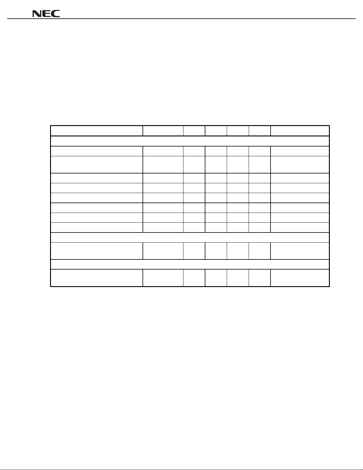
ORDERING INFORMATION
PART NUMBER PACKAGE SUPPLYING FORM
µ
PC8129GR-E1 20 pin plastic SSOP
(225 mil)
To order evaluation samples, please contact your local NEC sales office. (Part number for sample order:
*
PC8129GR)
µ
Caution electro-static sensitive device
The information in this document is subject to change without notice. Before using this document, please
confirm that this is the latest version.
Not all devices/types available in every country. Please check with local NEC representative for
availability and additional information.
Embossed tape 12 mm wide. QTY 2.5 kp/Reel.
Pins 1 through 10 are in pull-out direction.
Document No. P12781EJ2V0DS00 (2nd edition)
Date Published October 1999 N CP(K)
Printed in Japan
The mark shows major revised points.
©
1997, 1999
Page 2
INTERNAL BLOCK DIAGRAM AND PIN CONNECTIONS
µµµµ
PC8129GR
Up-Con in
Up-Con inb
MODout
Qb
LO1 in
LO1 inb
GND
1
2
3
I
4
Ib
5
6
Q
7
8
9
10
90deg. Phase
Shifter ( 2)
Reg.
20
19
18
17
16
15
14
13
12
11
VCC (MOD)
V
CC
(Up-con)
RFout
GND
V
PS
V
AGC
GND
LO2 in
LO2 inb
GND
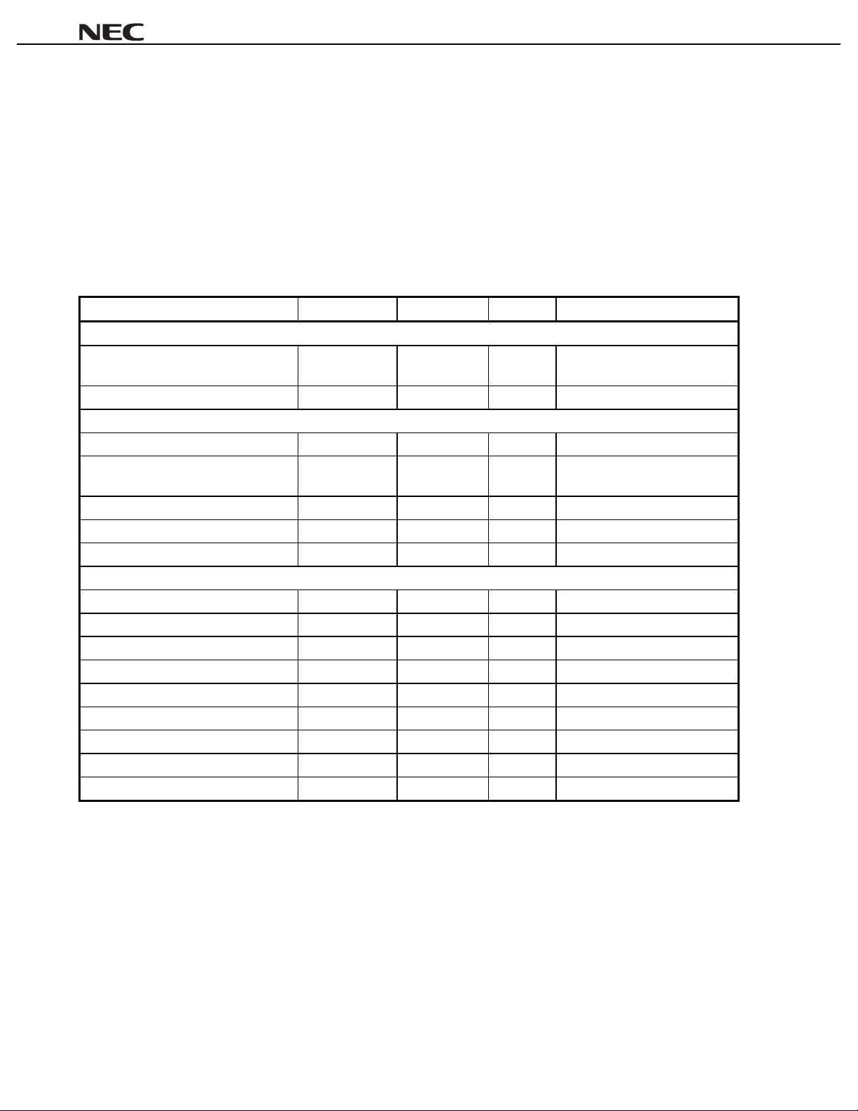
QUADRATURE MODULATOR SERIES PRODUCT
CC
Part Number Functions
PC8101GR 150 MHz Quad.Mod
µ
PC8104GR RF Up-Converter + IF
µ
I
(mA)
15/@2.7 V
28/@3.0 V
Quad.Mod
PC8105GR 400 MHz Quad.Mod
µ
PC8110GR 1 GHz Direct Quad.Mod
µ
PC8125GR RF Up-Converter + IF
µ
16/@3.0 V
24/@3.0 V
36/@3.0 V
Quad.Mod + AGC
PC8126GR 915 to 960 915 to 960
µ
PC8126K
µ
PC8129GR
µ
900 MHz Direct Quad.Mod
with Offset-Mixer
2LO IF Quad. Mod+RF
×
35/@3.0 V
28/@3.0 V
Up-Converter
µ
PC8139GR-7JH
PC8158K RF Up-Converter + IF
µ
Transceiver IC
(1.9 GHz Indirect Quad.
Mod + RX-IF + IF VCO)
TX: 32.5
RX: 4.8
/@3.0 V
28/@3.0 V
Quad.Mod + AGC
LO1in
f
(MHz)
100 to 300 50 to 150
MODout
f
(MHz)
100 to 400
RF Mixer
RFout
f
External F/F CT-2 etc.
900 to 1 900
100 to 400 External
800 to 1 000 External
220 to 270
1 800 to 2 000
889 to 960 889 to 960
200 to 800 100 to 400
220 to 270
100 to 300
800 to 1 900
1 800 to 2 000
800 to 1 500
(MHz)
Phase
Shifter
Doubler
+ F/F
F/F
CR
Package Application
20-pin
SSOP (225 mil)
Digital Comm.
16-pin
SSOP (225 mil)
20-pin
SSOP (225 mil)
PDC800 MHz, etc.
PHS
PDC800 MHz
28-pin QFN
20-pin
SSOP (225 mil)
30-pin
GSM,
DCS1800, etc.
PHS
TSSOP (225 mil)
28-pin QFN
PDC800 M/1.5 G
2
Data Sheet P12781EJ2V0DS00
Page 3
APPLICATION EXAMPLE
[GSM]
SUB ANT
µµµµ
PC8129GR
MAIN ANT
TX
SW
SW
RX
LNA 1st MIX
PA
SW
AGC
1st. LO
PLL1 PLL2
MODout
= f
LO
/2
(F/F)
φ
2nd MIX
2nd. LO
0 °
90 °
PC8129GR
µ
DEMO.
LO
f
I
Q
I
Q
Data Sheet P12781EJ2V0DS00
3
Page 4
ABSOLUTE MAXIMUM RATINGS
PARAMETER SYMBOL RATING UNIT CONDITION
µµµµ
PC8129GR
Supply Voltage V
Power Save Voltage V
AGC Control Voltage V
CC
PS
AGC
6.0 V TA = +25 °C
6.0 V
6.0 V
IQ DC Offset Voltage IQ (DC) 4.0 V
Power Dissipation P
Operating Ambient Temperature T
Storage Temperature T
Mounted on double sided copper clad 50 × 50 × 1.6 mm epoxy glass PWB.
Note
D
A
stg
430 mW
–40 to +85 °C
–55 to +150 °C
RECOMMENDED OPERATING CONDITIONS
PARAMETER SYMBOL MIN. TYP. MAX. UNIT CONDITIONS
Supply Voltage V
Operating Ambient Temperature T
Up Converter RF Frequency f
Up Converter Input Freq. f
Modulator Output Frequency f
LO1 Input Frequency f
LO1 Input Level P
LO2 Input Frequency f
LO2 Input Level P
I/Q Input Frequency f
I/Q Input Amplitude V
CC
A
RFout
UPCONin
MODout
LO1in
LO1in
LO2in
LO2in
I/Qin
I/Qin
2.7 3.0 5.5 V
–40 +25 +85 °C
800 1900 MHz
100 400 MHz
200 800 MHz
–15 –10 –5 dB m
800 1800 MHz
–15 –10 –5 dB m
DC 10 M Hz
600 mV
A
= +85 °C
T
P-P
Single ended Input
Note
4
Data Sheet P12781EJ2V0DS00
Page 5
ELECTRICAL CHARACTERISTICS (1)
Conditions (unless otherwise specified):
TA = +25 °C, VCC = 3 V, VPS = 3 V, RPS = 1 kΩ, V
AGC
= 3 V, R
I/Q DC = 1.5 V (Vbias(I) = Vbias(Ib) = Vbias (Q) = Vbias (Qb) = 1.5 V)
I/Qin
f
= 67.7 kHz, V
I/Qin
= 500 mV
P-P
(single ended input, Ib = Qb = 0 mV
Modulation Pattern: <0000>
LO1in
f
= 500 MHz, P
LO2in
f
= 1150 MHz, P
UPCONin
f
RFout
f
MODout
= f
= 900 MHz – f
PARAMETER SYMBOL MIN. TYP. MAX. UNIT TEST CONDITIONS
UP CONVERTER + QUADRATURE MODULATOR TOTAL
Total Circuit Current I
Total Circuit Current at Power S ave
Mode
Total Output Power P
Local Oscillator Carrier Leakage LoL –40 –26.5 dBc f
Image Rejection (Side Band Leak ) ImR –30 –26.5 dBc
AGC Gain Control Rang GCR 28 40 dB V
Power Save Rise Time TPS(rise) 2.0 5.0
Power Save Fall Time TPS(fall) 2.0 5.0
UP CONVERTER BLOCK
Circuit Current at Power Save Mode I
QUADRATURE MODULATOR BLOCK
Circuit Current at Power Save Mode I
= f
LO1in
= –10 dBm
LO2in
= –10 dBm
LO1in
/2 + f
I/Qin
I/Qin
= 250 MHz + f
CC(TOTAL)
CC(PS)TOTAL1
I
(Up con.)
(MOD)
RFout
CC(PS)
CC(PS)
I/Qin
20 28 37 mA No input signal
–8 –5 –2 dBm
AGC
= 10 k
0.6 10
Ω
P-P
5.0
5.0
)
AVPS ≤ 0.5 V
µ
sVPS(Low) → VPS(High)
µ
sVPS(High) → VPS(Low)
µ
AVPS ≤ 0.5 V
µ
AVPS ≤ 0.5 V
µ
µµµµ
PC8129GR
LoL
LO2
= f
AGC
LO1
– f
/2
= 2.5 V to 0 V
Data Sheet P12781EJ2V0DS00
5
Page 6
STANDARD CHARACTERISTICS FOR REFERENCE (1)
Conditions (unless otherwise specified):
TA = +25 °C, VCC = 3 V, VPS = 3 V, RPS = 1 kΩ, V
AGC
= 3 V, R
I/Q DC = 1.5 V (Vbias(I) = Vbias(Ib) = Vbias (Q) = Vbias (Qb) = 1.5 V)
I/Qin
f
= 67.7 kHz, P
I/Qin
= 500 mV
P-P
(single ended input, Ib = Qb = 0 mV
Modulation Pattern: <0000>
LO1in
f
= 500 MHz, P
LO2in
f
= 1150 MHz, P
UPCONin
f
RFout
f
MODout
= f
= 900 MHz – f
PARAMETER SYMBOL REFERENCE UNIT TEST CONDITIONS
UP CONVERTER + QUADRATURE MODULATOR TOTAL
Total Circuit Current at Power-S ave
Mode
Phase Error
UP CONVERTER BLOCK
UP Con. Circuit Current I
UP Con. Circuit Current at Power-Save
Mode
Conversion Gain CG 12 dB P
Maximum Output Power P
Output 3rd Order Intercept Point OIP
QUADRATURE MODULATOR BLOCK
MOD. Circuit Current I
Output Power P
LO1 Carrier Leakage LoL –40 dBc f
Image Rejection (Side Band Leak ) ImR –30 dBc
I/Q 3rd Order Intermodulation Dis tortion IM
I/Q Input Impedance Z
IQ Bias Current I
LO1 Input VSWR VSWR
Output Noise Floor –133 dB c /Hz
= f
LO1in
= –10 dBm
LO2in
= –10 dBm
LO1in
/2 + f
I/Qin
I/Qin
= 250 MHz + f
CC(PS)TOTAL2
I
CC(PS)UpCon
I
I/Qin
∆φ
CC(UpCon)
RF(sat)
3
CC(MOD)
MODout
3I/Q
I/Q
I/Q
(Lo1)
AGC
= 10 k
Ω
P-P
)
60
AVPS ≤ 0.5 V, V
µ
1.8 deg. (rms) MOD Pattern: PN9
14 mA No input signal
60
AVPS ≤ 0.5 V, V
µ
–1.5 dBm P
+6 dBm f
14 mA No input signal
–16.5 dBm
–50 dBc
200 k
5
Ω
A I, Ib, Q, Qb to GND (each)
µ
1.2 : 1 –
AGC
AGC
UPCONin
= –20 dBm
UPCONin
= –4 dBm
UPCONin
= 250.0 MHz/250.2 MHz
LoL
LO1
= f
/2
I to Ib, Q to Qb
f = ±20 MHz
∆
µµµµ
PC8129GR
= 0 V
= 0 V
6
Data Sheet P12781EJ2V0DS00
Page 7
STANDARD CHARACTERISTICS FOR REFERENCE (2)
Conditions (unless otherwise specified):
TA = +25 °C, VCC = 3 V, VPS = 3 V, RPS = 1 kΩ, V
AGC
= 3 V, R
I/Q DC = 1.5 V (Vbias(I) = Vbias(Ib) = Vbias (Q) = Vbias (Qb) = 1.5 V)
I/Qin
f
= 67.7 kHz, P
I/Qin
= 500 mV
P-P
(single ended input, Ib = Qb = 0 mV
Modulation Pattern: <0000>
LO1in
f
= 500 MHz, P
LO2in
f
= 1650 MHz, P
UPCONin
f
RFout
f
MODout
= f
= 1900 MHz + f
PARAMETER SYMBOL REFERENCE UNIT TEST CONDITIONS
UP CONVERTER + QUADRATURE MODULATOR TOTAL
Total Output Power P
Local Oscillator Carrier Leakage LoL –40 dBc f
Image Rejection (Side Band Leak ) ImR –30 dB c
AGC Gain Control Rang GCR 45 dB V
Phase Error
UP CONVERTER BLOCK
Conversion Gain CG 5 dB P
Maximum Output Power P
Output Intercept Point OIP
= f
LO1in
= –10 dBm
LO2in
= –10 dBm
LO1in
/2 + f
I/Qin
I/Qin
= 250 MHz + f
I/Qin
RFout
∆φ
RF(sat)
3
AGC
= 10 k
Ω
P-P
–12 dBm
1.8 deg. (rms) MOD Pattern: PN9
–7 dBm P
–1 dBm f
µµµµ
PC8129GR
)
LoL
LO2
= f
AGC
UPCONin
UPCONin
UPCONin
LO1
+ f
/2
= 2.5 V to 0 V
= –20 dBm
= –4 dBm
= 250.0 MHz/250.2 MHz
Data Sheet P12781EJ2V0DS00
7
Page 8
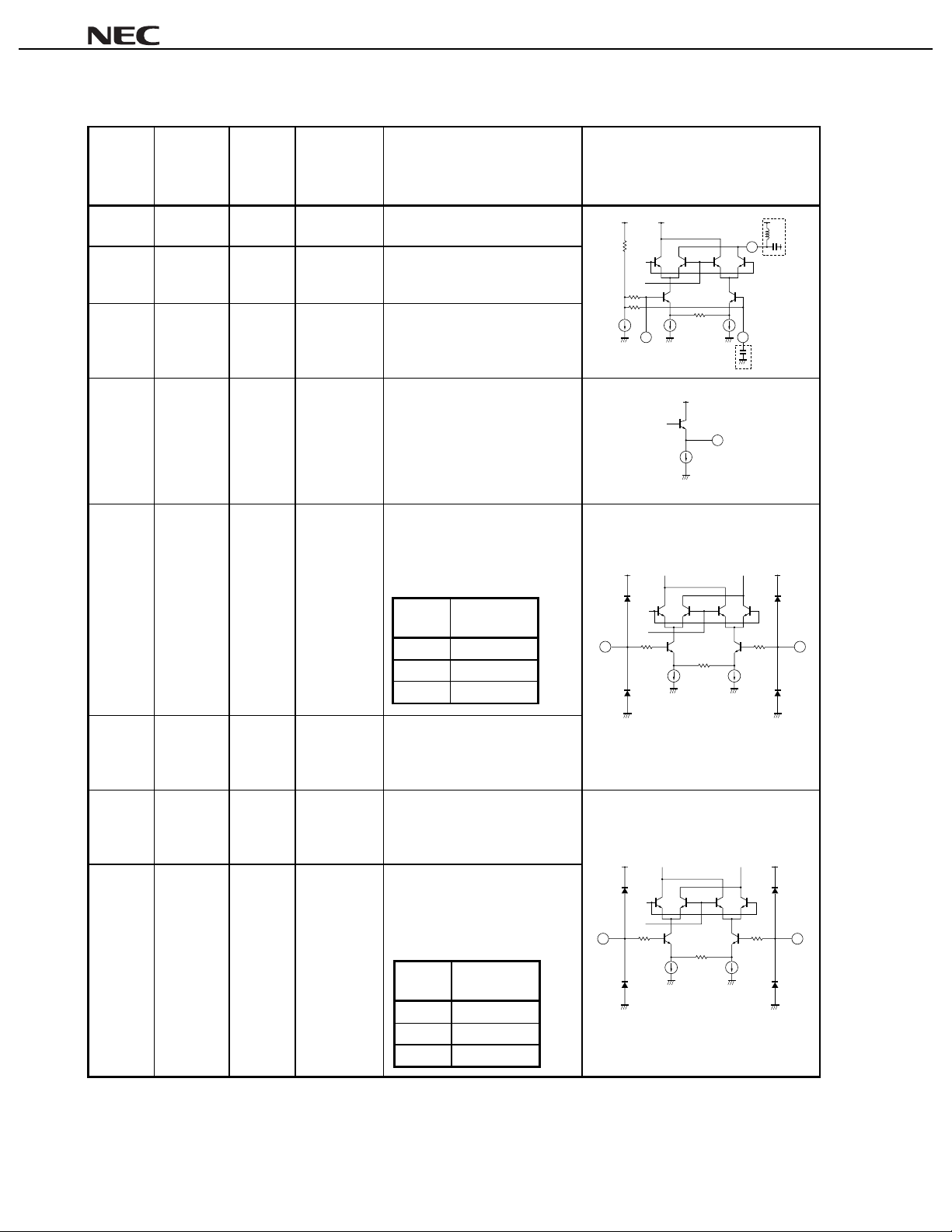
PIN EXPLANATION
µµµµ
PC8129GR
Pin
Voltage
Description Equivalent Circuit
Typ. (V)
CC
@V
= 3 V
CC
– RF output from Up-Converter.
Pin No. Symbol
18 RFout V
Supply
Voltage
(V)
This pin is open collect or out put.
1 UpCon in – 2.2 IF input for Up-converte r.
This pin is high impedance
input.
2 UpCon inb – 2.2 Bypass of IF input .
Grounded through external
capacitor.
3 MODout – 1.9 Output from modulator.
This is emitter follower output.
4IV
CC
/2 – Input for I signal. This input
impedance is about 200 kΩ.
Relations between amplitude
CC
and V
/2 bias of input signal
are following.
CC
/2
(V)
1.5
Signal Level
(mV
≤
≤
1000
≤
V
1.35
≥
≥
1.75
≥
P-P
400
600
18
1 2
3
Note
)
4 5
5IbV
CC
/2 – Input for I signal. This input
impedance is about 200 kΩ.
CC
V
/2 biased DC signal should
be input.
6QbV
CC
/2 – Input for Q signal. This i nput
impedance is about 200 k
CC
/2 biased DC signal should
V
Ω
be input.
7QV
CC
/2 – Input for Q signal. This i nput
impedance is about 200 kΩ.
Relations between amplitude
CC
and V
/2 bias of input signal
are following.
In the case of that I/Q input signals are single ended.
Note
VCC/2
(V)
1.35
≥
≥
1.75
≥
1.5
Signal Level
P-P
(mV
)
400
≤
600
≤
1000
≤
Note
Of course, I/Q signal inputs can be used either single endedly or differentially with proper terminations.
67
8
Data Sheet P12781EJ2V0DS00
Page 9
PIN EXPLANATION
µµµµ
PC8129GR
Pin
Voltage
Typ. (V)
CC
@V
Description Equivalent Circuit
= 3 V
Pin No. Symbol
Supply
Voltage
(V)
8 LO1in – 0 Lo1 input for phase shifter.
This input impedance is 50
matched internally.
9 LO1in b – 2.3 Bypass of Lo1 input.
This pin is grounded through
internal capacitor.
10
11
GND for
Modulator
0 – Connect to the ground with
minimum inductance.
Track length should be kept as
short as possible.
12 LO2in b – 1. 9 Bypass of Lo2 input.
Grounded through external
capacitor.
13 LO2i n – 1.9 Lo2 input of Up-converter.
This pin is high impedance input.
14
17
GND for
Up-con.
0 – Connect to the ground with
minimum inductance.
Track length should be kept as
short as possible.
15 V
AGC
0 to V
CC
– Input for AGC amplifier.
Total Output Power can be
controlled by changing input
voltage.
And as external series resistance
AGC
(R
) connecting, a slope of
AGC curve can be changed by
AGC
16 Power
Save
0 to V
the resistance (R
CC
– Power save control pin can be
controlled ON/OFF state with
bias as follows;
Ω
8
50 Ω
9
13
12
).
16
19 VCC for
Upconverter
20 VCC for
Modulator
: Externally
VPS (V) STATE
2 to VCCON (Active Mode)
0 to 0.5 OFF (Sleep Mode)
2.7 to 5.5 – Supply voltage pin for Upconverter.
2.7 to 5.5 – Supply voltage pin for modulator.
Internal regulator can be kept
stable condition of suppl y bias
against the variable
temperature or V
Data Sheet P12781EJ2V0DS00
CC
.
9
Page 10

µµµµ
STANDARD TYPICAL CHARACTERISTICS <Modulator + Up-Converter Total at 900 MHz>
PC8129GR
Test Circuit 1, TA = +25 °C, VCC = 3 V, VPS = 3 V, RPS = 1 kΩ, V
AGC
= 3 V, R
I/Q DC = 1.5 V (Vbias(I) = Vbias(Ib) = Vbias(Q) = Vbias(Qb) = 1.5 V)
I/Qin
f
= 67.7 kHz, V
Modulation Pattern: All Zero <0000>, f
LO2in
f
= 1150 MHz, P
RFout
f
= 900 MHz – f
40
30
20
- Total Circuit Current - mA
10
CC
I
0
0123456
I/Qin
= 500 mV
LO2in
I/Qin
ICC (TOTAL) vs V
No input signal
VCC - Supply Voltage - V
P-P
(single ended input, Ib = Qb = 0 mV
LO1in
= 500 MHz, P
= –10 dBm, f
UPCONin
= f
MODout
, Unless Otherwise Specified
CC
= f
LO1in
LO1in
/2 + f
= –10 dBm
I/Qin
AGC
= 10 k
Ω
P-P
)
= 250 MHz + f
I/Qin
ICC (TOTAL) vs V
PS
30
20
10
- Total Circuit Current - mA
CC
I
0
0123
TA = +25 °C
:
T
A
= +85 °C
:
T
A
= –40 °C
:
No input signal
VPS - Power Save Control Voltage - V
ICC (TOTAL) vs T
No input signal
30
20
10
- Total Circuit Current - mA
CC
I
0
–40 –20 0 +20 +40 +60 +80
TA - Operating Ambient Temperature - °C
A
ICC (PS) TOTAL vs T
A
µ
No input signal
Vps = 0.5 V
30
20
10
- Total Circuit Current at Power Save Mode - A
CC
0
I
–40 –20 0 +20 +40 +60 +80
TA - Operating Ambient Temperature - °C
10
Data Sheet P12781EJ2V0DS00
Page 11

µµµµ
PC8129GR
µ
ICC (PS) TOTAL2 vs T
150
A
No input signal
Vps = 0.5 V
125
V
AGC
= 0 V
100
75
50
25
- Total Circuit Current at Power Save Mode - A
CC
I
0
–20 0 +20 +40 +60 +80
–40
TA - Operating Ambient Temperature - °C
I
CC
µ
(PS) TOTAL2 vs V
150
CC
No input signal
Vps = 0.5 V
125
V
AGC
= 0 V
ICC (PS) TOTAL1 vs V
CC
µ
No input signal
Vps = 0.5 V
2
1
- Total Circuit Current at Power Save Mode - A
CC
I
0
0246
VCC - Supply Voltage - V
100
75
50
25
- Total Circuit Current at Power Save Mode - A
CC
I
0
0246
VCC - Supply Voltage - V
P
RFout
, LoL, ImR, IM
0
3I/Q
P
vs V
RFout
CC
–20
ImR
–10
–20
- Total Output Power - dBm
RFout
P
–30
LoL
IM
3I/Q
–30
–40
–50
P
RFout
, LoL, ImR, IM
0
P
–10
–20
- Total Output Power - dBm
RFout
P
LoL
RFout
ImR
IM
3I/Q
3I/Q
vs T
A
–20
–30
–40
0123456
VCC - Supply Voltage - V
Data Sheet P12781EJ2V0DS00
- I/Q 3rd Order Intermodulation Distortion - dBc
3I/Q
LoL - Local Oscillator Carrier Leakage - dBc
ImR - Image Rejection - dBc
IM
–40 –20 0 +20 +40 +60 +80
TA - Operating Ambient Temperature - °C
–50
- I/Q 3rd Order Intermodulation Distortion - dBc
3I/Q
LoL - Local Oscillator Carrier Leakage - dBc
ImR - Image Rejection - dBc
IM
11
Page 12

P
RFout
, LoL, ImR, IM
3I/Q
vs V
I/Qin
P
RFout
, LoL, ImR, IM
3I/Q
vs P
µµµµ
PC8129GR
LO1in
0
–10
–20
LoL
ImR
P
RFout
–30
- Total Output Power - dBm
RFout
–40
P
IM
3I/Q
100 500 1000 2000
V
I/Qin
- I/Q Input Amplitude - mVp-p
P
RFout
0
–10
vs P
LO2in
–20
–30
–20
–30
–40
–50
–60
LoL - Local Oscillator Carrier Leakage - dBc
ImR - Image Rejection - dBc
–70
–40
- I/Q 3rd Order Intermodulation Distortion - dBc
- I/Q 3rd Order Intermodulation Distortion - dBc
–50
3I/O
3I/O
LoL - Local Oscillator Carrier Leakage - dBc
ImR - Image Rejection - dBc
IM
IM
–30 –20 –10 0 +10
7
MOD Pattern: PN9
6
5
4
RFout
P
P
LO1in
- LO1 Input Level - dBm
vs V
∆Φ
ImR
I/Qin
IM
3I/Q
LoL
0
–10
–20
- Total Output Power - dBm
RFout
P
–30
–20
- Total Output Power - dBm
–30
RFout
P
–40
–40 –20 –10 0–30
P
LO2in
- LO2 Input Level - dBm
P
RFout
+10
0
–10
–20
–30
T
A
–40
- Total Output Power - dBm
–50
RFout
P
–60
= +85 °C
+25 °C
–40 °C
vs V
AGC
3
2
∆Φ
- Phase Error - deg. (rms.)
1
0
100 500 1000
V
I/Qin
- I/Q Input Amplitude - mV
P
RFout
0
–10
–20
–30
–40
- Total Output Power - dBm
RFout
P
–50
= 2.7 V
CC
V
= 3 V
CC
V
GCR
= 40.5 dB
(V
CC
= 2.7 V)
vs V
GCR
= 40.8 dB
CC
= 3 V)
(V
AGC
P-P
= 5.5 V
CC
V
GCR
= 41.7 dB
(V
CC
= 5.5 V)
–70
12
0231
V
AGC
- AGC Control Voltage - V
–60
0231456
Data Sheet P12781EJ2V0DS00
V
AGC
- AGC Control Voltage - V
Page 13

+10
–10
µµµµ
PC8129GR
P
RFout
vs V
AGC
µ
PC8129GR
REF 0.0 dBm
10 dB/
POWER SAVE RESPONSE
ATT 10dB
0
–20
–30
–40
- Total Output Power - dBm
RFout
P
–50
–60
0
= 80 kΩ, SLOPE = 53 dB/V
AGC
R
123
V
AGC
- AGC Control Voltage - V
GCR =
39.8 dB
= 10 kΩ, SLOPE = 143 dB/V
AGC
R
RBW
3 MHz
VBW
3 MHz
SWP
µ
50 s
CENTER 900.0677 MHz SPAN 0 Hz
TYPICAL SINE WAVE MODULATION OUTPUT SPECTRUM TYPICAL GMSK MODULATION OUTPUT SPECTRUM
µ
PC8129GR
REF 0.0 dBm
10 dB/
ATT 10 dB
1
µ
PC8129GR
REF –10.0 dBm
10 dB/
ATT 0 dB
A write B view
MARKER
899.200 MHz
–77.25 dB
3
4
ADJ BS
135 kHz
2
DL –10.0 dBm
1
3 4
2
5 6
RBW 3 kHz
VBW 10 kHz
SWP 1.0 s
CENTER 900.0000 MHz SPAN 500 KHz
Multi Marker List
No.1:
No.2:
No.3:
No.4:
***
899.9323 MHz
900.0000 MHz
900.0677 MHz
900.2031 MHz
***
–4.80 dBm
–48.02 dBc
–29.88 dBc
–42.41 dBc
TYPICAL SINE WAVE MODULATION OUTPUT SPECTRUM
3
f
LO1in
2
(= 3fIF)
ATT 10 dB
f
LO2in
2 f
LO1in
(= 4fIF)
5
f
LO1in
2
(=
IF
)
5f
MARKER
900 MHz
–4.67 dBm
µ
PC8129GR
REF 0.0 dBm
10 dB/
RBW 300 kHz
VBW 300 kHz
SWP 5.0 s
1
f
LO1in
2
(= fIF)
f
LO1in
(= 2fIF)
START 0 Hz STOP 2.460 GHz
RBW 3 kHz
VBW 10 kHz
SWP 5.0 s
CENTER 900. 000 MHz SPAN 2.000 MHz
No.1:
No.2:
No.3:
No.4:
No.5:
No.6:
TYPICAL SINE WAVE MODULATION OUTPUT SPECTRUM
∆:
Multi Marker List
***
899.200 MHz
899.400 MHz
899.600 MHz
900.400 MHz
900.600 MHz
900.800 MHz
***
–77.25 dB
–76.50 dB
–68.00 dB
–68.25 dB
–77.50 dB
–77.50 dB
(IN BAND)
µ
PC8129GR
REF 0.0 dBm
10 dB/
MKR 900 MHz
RBW 300 kHz
VBW 300 kHz
SWP 5.0 s
750 MHz
–43.6 dBm
800 MHz
–49.5 dBm
CENTER 900.0 MHz SPAN 400.0 MHz
ATT 10 dB
850 MHz
–56.6 dBm
950 MHz
–68.2 dBm
1000 MHz
–53.0 dBm
MARKER
900 MHz
–4.68 dBm
1050 MHz
–59.4 dBm
Data Sheet P12781EJ2V0DS00
13
Page 14

µµµµ
TYPICAL SINE WAVE MODULATION OUTPUT SPECTRUM
(IN BAND)
TYPICAL SINE WAVE MODULATION OUTPUT SPECTRUM
(IN BAND)
TYPICAL SINE WAVE MODULATION OUTPUT SPECTRUM
(IN BAND)
ATT 10 dB
RBW 300 kHz
VBW 300 kHz
SWP 5.0 s
CENTER 920.0 MHz SPAN 200.0 MHz
PC8129GR
REF 0.0 dBm
10 dB/
µ
MARKER
880.0 MHz
–4.64 dBm
870 MHz
–55.7 dBm
890 MHz
–63.0 dBm
1000 MHz
–54.8 dBm
1010 MHz
–57.6 dBm
f
LO1in
= 500 MHz
(f
MODout
= 250 MHz
+ f
I/Q
)
f
LO2
= 1130 MHz
f
RFout
= 880 MHz
ATT 10 dB
RBW 300 kHz
VBW 300 kHz
SWP 5.0 s
CENTER 920.0 MHz SPAN 200.0 MHz
PC8129GR
REF 0.0 dBm
10 dB/
µ
MARKER
900 MHz
–4.66 dBm
850 MHz
–56.2 dBm
950 MHz
–65.5 dBm
1000 MHz
–53.0 dBm
MKR 900 MHz
ATT 10 dB
RBW 300 kHz
VBW 300 kHz
SWP 5.0 s
CENTER 920.0 MHz SPAN 200.0 MHz
PC8129GR
REF 0.0 dBm
10 dB/
µ
MARKER
900 MHz
–7.41 dBm
f
LO1in
= 500 MHz
(f
MODout
= 250 MHz
+ f
I/Qin
)
f
LO2in
= 1210 MHz
f
RFout
= 960 MHz
– f
I/Qin
MKR 900 MHz
880 MHz
–59.9 dBm
920 MHz
–51.5 dBm
1000 MHz
–49.9 dBm
PC8129GR
14
Data Sheet P12781EJ2V0DS00
Page 15

µµµµ
PC8129GR
STANDARD TYPICAL CHARACTERISTICS <Modulator + Up-Converter Total at 1900 MHz>
Test Circuit 2, TA = +25 °C, VCC = 3 V, VPS = 3 V, RPS = 1 kΩ, V
AGC
= 3 V, R
I/Q DC = 1.5 V (Vbias(I) = Vbias(Ib) = Vbias(Q) = Vbias(Qb) = 1.5 V)
I/Qin
f
= 67.7 kHz, V
Modulation Pattern: All Zero <0000>, f
LO2in
f
= 500 MHz, P
RFout
f
= 1900 MHz + f
0
–10
–20
–30
–40
–50
- Total Output Power - dBm
RFout
P
–60
–70
0
I/Qin
= 500 mV
LO2in
= –10 dBm, f
I/Qin
, Unless Otherwise Specified
P
RFout
P-P
(single ended input, Ib = Qb = 0 mV
LO1in
= 500 MHz, P
vs V
UPCONin
AGC
= f
MODout
GCR =
= 80 kΩ, SLOPE = 59 dB/V
AGC
R
AGC
R
= 10 kΩ, SLOPE = 154 dB/V
45.4 dB
123
V
AGC
- AGC Control Voltage - V
= f
LO1in
LO1in
= –10 dBm
I/Qin
/2 + f
AGC
= 10 k
Ω
P-P
)
= 250 MHz + f
I/Qin
P
RFout
0
–10
–20
–30
- Total Output Power - dBm
–40
RFout
P
100 500 1000 2000
V
I/Qin
- I/Q Input Amplitude - mV
vs V
I/Qin
P-P
P
RFout
vs P
LO1in
0
–10
–20
- Total Output Power - dBm
RFout
P
–30
–30 –20 –10 0 +10
P
LO1in
- LO1 Input Level - dBm
P
RFout
0
–10
–20
- Total Output Power - dBm
RFout
P
–30
–40 –30 –10 0 +10–20
P
LO2in
- LO2 Input Level - dBm
vs P
LO2in
Data Sheet P12781EJ2V0DS00
15
Page 16

µµµµ
PC8129GR
TYPICAL SINE WAVE MODULATION OUTPUT SPECTRUM
µ
PC8129GR
REF 0.0 dBm
10 dB/
ATT 10 dB
1
7
MOD Pattern: PN9
6
Φ vs V
∆
I/Qin
5
3
4
4
2
3
2
Φ - Phase Error - deg. (rms)∆
1
0
100
V
I/Qin
- I/Q Input Amplitude - mVp-p
500 1000 2000
RBW 3 kHz
VBW 10 kHz
SWP 1.0 s
CENTER 1.9000000 GHz SPAN 500 kHz
Multi Marker List
No.1:
No.2:
No.3:
No.4:
***
1.9000677 GHz
1.9000000 GHz
1.8999323 GHz
1.8997969 GHz
***
–12.13 dBm
–39.30 dBc
–28.98 dBc
–41.30 dBc
TYPICAL GMSK MODULATION OUTPUT SPECTRUM TYPICAL SINE WAVE MODULATION OUTPUT SPECTRUM
3
f
2
(= 3fIF)
LO1in
ATT 10 dB
2 f
LO1in
(= 4fIF)
5
f
2
(= 5fIF)
LO2in
f
LO1in
7
3 f
LO1in
f
LO1in
2
(= 6fIF)
(= 7fIF)
µ
PC8129GR
REF –10.0 dBm
10 dB/
MKR
1.899200 GHz
DL –10.0 dBm
ATT 0 dB
A write B view
MARKER
1. 899200 GHz
–74. 75 dB
µ
PC8129GR
REF 0.0 dBm
10 dB/
MKR 1.900 GHz
1
fLO1in
2
(= fIF)
fLO1in
(= 2fIF)
3
2
1
546
MARKER
1.900 GHz
–11. 67 dBm
4 f
LO1in
(= 8fIF)
RBW 3 kHz
VBW 10 kHz
SWP 5.0 s
CENTER 1.900000 GHz SPAN 2. 000 MHz
No.1:
No.2:
No.3:
No.4:
No.5:
No.6:
TYPICAL SINE WAVE MODULATION OUTPUT SPECTRUM
∆:
Multi Marker List
***
1.899200 GHz
1.899400 GHz
1.899600 GHz
1.900400 GHz
1.900600 GHz
1.900800 GHz
***
–74.75 dB
–74.50 dB
–64.75 dB
–66.50 dB
–74.25 dB
–74.75 dB
(IN BAND)
µ
PC8129GR
REF 0.0 dBm
10 dB/
ATT 10 dB
1
2
7
6
5
***
–11.71 dBm
–24.07 dBm
–64.52 dBm
–63.37 dBm
–61.09 dBm
–59.39 dBm
–31.62 dBm
RBW 300 kHz
VBW 300 kHz
SWP 5.0 s
4
3
CENTER 1.9000 GHz SPAN 600 MHz
Multi Marker List
***
No.1:
1.900 GHz
No.2:
1.650 GHz
No.3:
1.750 GHz
No.4:
1.800 GHz
No.5:
2.000 GHz
No.6:
2.050 GHz
No.7:
2.150 GHz
RBW 300 kHz
VBW 300 kHz
SWP 5.0 s
START 0 Hz STOP 2.500 GHz
TYPICAL SINE WAVE MODULATION OUTPUT SPECTRUM
(IN BAND)
µ
PC8129GR
REF 0.0 dBm
10 dB/
f
RFout
= 1.71 GHz
+ f
f
LO2in
= 1.46 GHz
I/Qin
ATT 10 dB
1
6
4
2
5
7
3
RBW 300 kHz
VBW 300 kHz
SWP 5.0 s
CENTER 1.7950 GHz SPAN 600 MHz
Multi Marker List
No.1:
No.2:
No.3:
No.4:
No.5:
No.6:
No.7:
***
1.710 GHz
1.670 GHz
1.750 GHz
1.920 GHz
1.940 GHz
1.960 GHz
2.000 GHz
***
–15.16 dBm
–61.50 dBm
–67.84 dBm
–46.33 dBm
–58.68 dBm
–27.94 dBm
–62.11 dBm
16
Data Sheet P12781EJ2V0DS00
Page 17

µµµµ
TYPICAL SINE WAVE MODULATION OUTPUT SPECTRUM
(IN BAND)
TYPICAL SINE WAVE MODULATION OUTPUT SPECTRUM
(IN BAND)
2
5
6
ATT 10 dB
RBW 300 kHz
VBW 300 kHz
SWP 5.0 s
CENTER 1.7950 GHz SPAN 600 MHz
PC8129GR
REF 0.0 dBm
10 dB/
µ
No.1:
No.2:
No.3:
No.4:
No.5:
No.6:
No.7:
1.795 GHz
1.545 GHz
1.590 GHz
1.750 GHz
1.840 GHz
2.000 GHz
2.045 GHz
–14.21 dBm
–24.47 dBm
–65.96 dBm
–66.40 dBm
–60.91 dBm
–61.79 dBm
–28.73 dBm
***
Multi Marker List
***
f
RFout
= 1.795 GHz
+ f
I/Qin
f
LO2in
= 1.545 GHz
1
2
3
4
5
6
ATT 10 dB
RBW 300 kHz
VBW 300 kHz
SWP 5.0 s
CENTER 1.7950 GHz SPAN 600 MHz
PC8129GR
REF 0.0 dBm
10 dB/
µ
No.1:
No.2:
No.3:
No.4:
No.5:
No.6:
1.880 GHz
1.630 GHz
1.750 GHz
1.760 GHz
2.000 GHz
2.010 GHz
–12.32 dBm
–23.47 dBm
–64.08 dBm
–63.19 dBm
–61.05 dBm
–60.25 dBm
***
Multi Marker List
***
f
RFout
= 1.88 GHz
+ f
I/Qin
f
LO2in
= 1.63 GHz
1
3 4
7
PC8129GR
Data Sheet P12781EJ2V0DS00
17
Page 18

STANDARD TYPICAL CHARACTERISTICS <Up-Converter Block>
µµµµ
PC8129GR
TA = +25 °C, VCC = 3.0 V, VPS = 3.0 V, f
Test Circuit 1 (f
Test Circuit 2 (f
RFout
RFout
f
UpConin
LO2in
f
0
RFout
f
= 900 MHz, f
= 1900 MHz, f
P
RFout
= 250.0/250.2 MHz
= 1.15 GHz
= 899.8/900.0 MHz
–10
–20
P
RFout
–30
–40
–50
- Output Power - dBm
RFout
–60
P
–70
- 3rd Order Intermoduration Distortion - dBm
3
IM
–50
–40 –30 –20 –10 0
P
UPCONin
- Up-Converter Input Level - dBm
LO2in
, IM3, vs P
IM
CG vs P
= 1150 MHz) or
LO2in
UpConin
3
LO2in
UPCONin
= 250 MHz, P
UPCONin
= –20 dBm
= 1650 MHz), Unless Otherwise Specified
f
OIP
3
= +5.8 dBm
- Output Power - dBm
RFout
P
UpConin
LO2in
= 1.65 GHz
f
0
RFout
= 1.9000/1.9002 GHz
f
–10
–20
–30
–40
–50
–60
–70
- 3rd Order Intermoduration Distortion - dBm
3
–80
IM
–50
P
UPCONin
P
RFout
, IM3, vs P
= 250.0/250.2 MHz
RFout
P
IM
UpConin
3
OIP
= –1.3 dBm
–40 –30 –20 –10 0
- Up-Converter Input Level - dBm
3
15
10
5
f
RFout
LO2in
f
CG - Conversion Gain - dB
0
–40 –30 –20 –10 0
P
LO2in
- LO2 Input Level - dBm
f
RFout
= 900 MHz
LO2in
= 1.15 GHz
f
= 1.9 GHz
= 1.65 GHz
18
Data Sheet P12781EJ2V0DS00
Page 19

STANDARD TYPICAL CHARACTERISTICS <Modulator Block>
Test Circuit 1 or 2, TA = +25 °C, VCC = 3 V, VPS = 3 V
I/Q DC = 1.5 V (Vbias(I) = Vbias(Ib) = Vbias(Q) = Vbias(Qb) = 1.5 V)
I/Qin
f
= 67.7 kHz, V
Modulation Pattern: All Zero <0000>, f
MODout
f
+10
= f
LO1in
/2 + f
I/Qin
= 500 mV
I/Qin
= 250 MHz + f
P
MODout
P-P
(single ended input, Ib = Qb = 0 mV
vs V
LO1in
= 500 MHz, P
I/Qin
, Unless Otherwise Specified
I/Qin
LO1in
P-P
= –10 dBm
+10
)
P
MODout
vs P
µµµµ
PC8129GR
LO1in
0
–10
–20
–30
- Moduration Output Power - dBm
–40
MODout
P
–50
100 200 500 20001000
V
I/Qin
- I/Q Input Amplitude - mV
P
MODout
, LoL, ImR, IM
0
–10
–20
P
RFout
LoL
3I/Q
vs f
LO1in
P-P
–20
–30
0
–10
–20
–30
- Moduration Output Power - dBm
–40
MODout
P
–50
–40
–30 –20 –10 0
P
LO1in
- LO1 Input Level - dBm
vs V
∆Φ
I/Qin
3
MOD Pattern: PN9
2
–30
ImR
–40
- Moduration Output Power - dBm
–50
MODout
P
IM
3I/Q
100 200 500 2000
f
LO1in
- LO1 Input Frequency - MHz
–40
–50
–60
1000 200
–70
Data Sheet P12781EJ2V0DS00
- I/Q 3rd Order Intermodulation Distortion - dBc
3I/Q
LoL - Local Oscillator Carrier Leakage - dBc
ImR - Image Rejection - dBc
IM
- Phase Error - deg. (rms.)∆Φ
1
100 500 1000 2000
V
I/Qin
- I/Q Input Amplitude - mV
P-P
19
Page 20

7
MOD Pattern: PN9
6
5
∆
Φ vs f
LO1in
µµµµ
PC8129GR
TYPICAL SINE WAVE MODULATION OUTPUT SPECTRUM
PC8129GR
µ
REF 0.0 dBm
10 dB/
ATT 10 dB
1
4
3
2
∆
Φ - Phase Error - deg. (rms.)
1
0
100
200 500
f
LO1in
- LO1 Input Frequency - MHz
1000 2000
RBW 3 kHz
VBW 10 kHz
SWP 1.0 s
3
2
4
CENTER 250.0000 MHz SPAN 500 kMHz
No.1:
No.2:
No.3:
No.4:
Multi Marker List
***
250.0677 MHz
250.0000 MHz
249.9323 MHz
249.7969 MHz
***
–16.37 dBm
–39.49 dBc
–31.07 dBc
–58.80 dBc
20
Data Sheet P12781EJ2V0DS00
Page 21

µµµµ
PC8129GR
LO1 INPUT (Pin8) IMPEDANCE
V
CC
= VPS = 3 V
CH1 S11 1 U FS 2: 47.998 Ω 0.8066 Ω 256.76 pH
MARKER 2
500 MHz
2
3
1
START 100.000 000 MHz STOP 1 000.000 000 MHz
500.000 000 MHz
MARKER
1:
200 MHz
2:
500 MHz
3:
800 MHz
Up-Con. INPUT (Pin1) IMPEDANCE
V
CC
= VPS = 3 V
11 1 U FS 2: 101.78 Ω –387.03 Ω 1.6449 pF
CH1 S
MARKER 2
250 MHz
250. 000 000 MHz
MOD OUTPUT (Pin3) IMPEDANCE
VCC = VPS = 3 V
22 1 U FS 2: 31.195 Ω 14.908 Ω 9.4909 nH
CH1 S
MARKER 2
250 MHz
2
3
1
START 50.000 000 MHz STOP 500.000 000 MHz
250.000 000 MHz
MARKER
1:
2:
3:
100 MHz
250 MHz
400 MHz
LO2 INPUT (Pin13) IMPEDANCE
VCC = VPS = 3 V
CH1 S
11 1 U FS 1: 22.379 Ω –93.543 Ω 1.8905 pF
MARKER 1
900 MHz
900.000 000 MHz
2
1
3
MARKER
1:
100 MHz
2:
250 MHz
3:
400 MHz
START 50.000 000 MHz STOP 500.000 000 MHz
RF OUTPUT (Pin18) IMPEDANCE
V
CC
= VPS = 3 V
CH1 S
22 1 U FS 1: 18.953 Ω –158.83 Ω 1.1134 pF
MARKER 1
900 MHz
START 800.000 000 MHz STOP 2 000.000 000 MHz
900.000 000 MHz
Connect to inductor
(L
between pin18 and
pin19
1
2
3
2
= 100 nH)
MARKER
1:
2:
3:
900 MHz
1150 MHz
1900 MHz
3
START 800.000 000 MHz STOP 2 000.000 000 MHz
1
2
MARKER
1:
900 MHz
2:
1150 MHz
3:
1900 MHz
Data Sheet P12781EJ2V0DS00
21
Page 22

µµµµ
PC8129GR
TEST CIRCUIT 1 (In the case of f
100 pF
1000 pF
1000 pF
(Open)
I(DC), V
Ib(DC)
Qb(DC)
Q(DC), V
LO1in
Notes 1.
100 pF
Iin
10 nF
10 nF
Qin
100 pF
50 Ω matching circuit at f
In the case of using NEC’s evaluation board.
50 Ω matching circuit at f
2.
In the case of using NEC’s evaluation board.
RFout
= 900 MHz Band)
1
Up-Con. in
2
Up-Con. inb
3
MODout
4
I
5
Ib
6
Qb
7
Q
8
LO1in
9
LO1inb
10
GND
LO2in
= 1150 MHz.
RFout
= 900 MHz.
VCC(MOD.)
V
CC
(UP-CON.)
RFout
GND
V
V
AGC
GND
LO2in
LO2inb
GND
V
CC
84 nH
10 nF
10 nF
V
f
RFout
CC
20
19
1000 pF
1000 pF
ZL = 50 Ω
18
15 nH
6 pF
17
RPS = 1 kΩ
PS
16
R
AGC
= 10 kΩ
15
14
Note 1
ZL = 50 Ω
Note 2
10 nF
100 pF
10 nF
Vps
V
AGC
LO2in
13
6.8 nH
4 pF
100 pF
12
100 pF
11
22
Data Sheet P12781EJ2V0DS00
Page 23

µµµµ
PC8129GR
TEST CIRCUIT 2 (In the case of f
100 pF
1000 pF
1000 pF
(Open)
10
I(DC), V
Ib(DC)
Qb(DC)
Q(DC), V
LO1in
Notes 1.
100 pF
Iin
10 nF
10 nF
Qin
100 pF
50 Ω matching circuit at f
In the case of using NEC’s evaluation board.
50 Ω matching circuit at f
2.
In the case of using NEC’s evaluation board.
RFout
= 1900 MHz Band)
1
Up-Con. in
2
Up-Con. inb
3
MODout
4
I
5
Ib
6
Qb
7
Q
8
LO1in
9
LO1inb
GND
LO2in
= 1650 MHz.
RFout
= 1900 MHz.
VCC(MOD.)
CC
(UP-CON.)
V
RFout
GND
V
V
AGC
GND
LO2in
LO2inb
GND
V
CC
68 nH
Note 2
10 nF
10 nF
100 pF
10 nF
10 nF
100 pF
V
CC
f
RFout
Vps
V
AGC
LO2in
20
19
18
17
16
PS
15
14
13
12
11
1000 pF
1000 pF
ZL = 50 Ω
3 pF
RPS = 1 kΩ
R
ZL = 50 Ω
2 pF
100 pF
AGC
= 10 kΩ
Note 1
Data Sheet P12781EJ2V0DS00
23
Page 24

EXAMPLE OF TEST CIRCUIT 1 ASSEMBLED ON EVALUATION BOARD
)
I/Qin
= 250 MHz + f
MODout
(f
= 900 MHz
= 1150 MHz
LO2in
RFout
f
f
= 500 MHz
LO1in
f
C = 10 nF
µµµµ
PC8129GR
AGC
V
PS
V
CC
V
C = 10 nF C = 10 nF C = 10 nF
C = 100 pF
C = 4 pF
AGC
R
= 10 kΩ
= 1 kΩ
PS
R
C = 100 pF
C = 6 pF
L =
84 nH
L = 6.8 nH
L = 15 nH
C = 1000 pF
C = 100 pF
C = 1000 pF
C = 1000 pF
C = 100 pF
C = 100 pF
C = 100 pF
C = 10 nF C = 10 nF
C = 10 nF
Ib Qb
Notes 1.
Double-sided patterning with 35
GND pattern on backside.
2.
Solder coating over patterns.
3.
4. ,
indicate through-holes.
m thick copper on 50 × 50 × 0.4 mm polyimide board.
µ
NOTICE The test circuits and board pattern on data sheet are for performance evaluation use only. In the
case of actual design-in, matching circuit should be determined using S-parameter of desired
frequency in accordance to actual mounting pattern.
24
Data Sheet P12781EJ2V0DS00
Page 25

EXAMPLE OF TEST CIRCUIT 2 ASSEMBLED ON EVALUATION BOARD
)
I/Qin
I/Qin
= 250 MHz + f
MODout
(f
= 1.9 GHz + f
= 1.65 GHz
LO2in
RFout
f
f
= 500 MHz
LO1in
f
µµµµ
PC8129GR
C = 10 nF
AGC
V
PS
V
CC
V
C = 10 nF C = 10 nF C = 10 nF
C = 100 pF
AGC
R
= 1 kΩ
PS
R
C = 3 pF
C = 100 pF
C = 2 pF
= 10 kΩ
L = 68 nH
C =
1000 pF
C = 100 pF
C = 1000 pF
C = 100 pF
C = 100 pF
C = 100 pF
C = 1000 pF C = 1000 pF
C = 10 nF
Ib Qb
Notes 1.
Double-sided patterning with 35
GND pattern on backside.
2.
Solder coating over patterns.
3.
4. ,
indicate through-holes.
m thick copper on polyimide board.
µ
NOTICE The test circuits and board pattern on data sheet are for performance evaluation use only. In the
case of actual design-in, matching circuit should be determined using S-parameter of desired
frequency in accordance to actual mounting pattern.
Data Sheet P12781EJ2V0DS00
25
Page 26

PACKAGE DIMENSIONS
20 PIN PLASTIC SSOP (225 mil) (UNIT: mm)
µµµµ
PC8129GR
20
110
6.7 ± 0.3
1.8 MAX.
1.5 ± 0.1
11
detail of lead end
3˚
6.4 ± 0.2
4.4 ± 0.1
+7˚
–3˚
1.0 ± 0.2
NOTE
0.5 ± 0.2
0.15
+0.10
–0.05
0.1 ± 0.1
0.65
0.22
+0.10
–0.05
0.10
0.15
M
0.575 MAX.
Each lead centerline is located within 0.10 mm of its true position (T.P.) at maximum material condition.
26
Data Sheet P12781EJ2V0DS00
Page 27

µµµµ
PC8129GR
NOTE ON CORRECT USE
(1) Observe precautions for handling because of electrostatic sensitive devices.
(2) Form a ground pattern as widely as possible to minimize ground impedance (to prevent undesired oscillation).
(3) Keep the track length of the ground pins as short as possible.
(4) Connect a bypass capacitor (e.x. 1000 pF) to the VCC pin.
RECOMMENDED SOLDERING CONDITIONS
This product should be soldered in the following recommended conditions. Other soldering method and
conditions than the recommended conditions are to be consulted with sales representatives.
PC8129GR
µµµµ
Soldering process Soldering conditions Symbol
Infrared ray reflow Peak package’s surface temperat ure: 235 °C or below,
Reflow time: 30 seconds or bel ow (210 °C or higher)
Number of reflow process: 2, Exposure limit
VPS Peak package’s surface temperature: 215 °C or below,
Reflow time: 40 seconds or bel ow (200 °C or higher)
Number of reflow process: 2, Exposure limit
Wave soldering Solder temperature: 260 °C or below,
Flow time: 10 seconds or below,
Number of flow process: 1, Exposure limit
Partial heating method Terminal temperature: 300 °C or bel ow,
Flow time: 3 seconds/pi n or bel ow,
Exposure limit
Exposure limit before soldering after dry-pack package is opened.
Note
Note
: None
Note
Note
Note
: None
: None
: None
Storage conditions: 25 °C and relative humidity at 65 % or less.
Caution Apply only a single process at once, except for “Partial heating method”.
For details of recommended soldering conditions for surface mounting, refer to information
document SEMICONDUCTOR DEVICE MOUNTING TECHNOLOGY MANUAL (C10535E).
IR35-00-2
VP15-00-2
WS60-00-1
Data Sheet P12781EJ2V0DS00
27
Page 28

µµµµ
PC8129GR
• The information in this document is subject to change without notice. Before using this document, please
confirm that this is the latest version.
• No part of this document may be copied or reproduced in any form or by any means without the prior written
consent of NEC Corporation. NEC Corporation assumes no responsibility for any errors which may appear in
this document.
• NEC Corporation does not assume any liability for infringement of patents, copyrights or other intellectual property
rights of third parties by or arising from use of a device described herein or any other liability arising from use
of such device. No license, either express, implied or otherwise, is granted under any patents, copyrights or other
intellectual property rights of NEC Corporation or others.
• Descriptions of circuits, software, and other related information in this document are provided for illustrative
purposes in semiconductor product operation and application examples. The incorporation of these circuits,
software, and information in the design of the customer's equipment shall be done under the full responsibility
of the customer. NEC Corporation assumes no responsibility for any losses incurred by the customer or third
parties arising from the use of these circuits, software, and information.
• While NEC Corporation has been making continuous effort to enhance the reliability of its semiconductor devices,
the possibility of defects cannot be eliminated entirely. To minimize risks of damage or injury to persons or
property arising from a defect in an NEC semiconductor device, customers must incorporate sufficient safety
measures in its design, such as redundancy, fire-containment, and anti-failure features.
• NEC devices are classified into the following three quality grades:
"Standard", "Special", and "Specific". The Specific quality grade applies only to devices developed based on a
customer designated "quality assurance program" for a specific application. The recommended applications of
a device depend on its quality grade, as indicated below. Customers must check the quality grade of each device
before using it in a particular application.
Standard: Computers, office equipment, communications equipment, test and measurement equipment,
audio and visual equipment, home electronic appliances, machine tools, personal electronic
equipment and industrial robots
Special: Transportation equipment (automobiles, trains, ships, etc.), traffic control systems, anti-disaster
systems, anti-crime systems, safety equipment and medical equipment (not specifically designed
for life support)
Specific: Aircraft, aerospace equipment, submersible repeaters, nuclear reactor control systems, life
support systems or medical equipment for life support, etc.
The quality grade of NEC devices is "Standard" unless otherwise specified in NEC's Data Sheets or Data Books.
If customers intend to use NEC devices for applications other than those specified for Standard quality grade,
they should contact an NEC sales representative in advance.
M7 98. 8
 Loading...