

Page 1
DATA SHEET
BIPOLAR ANALOG INTEGRATED CIRCUIT
µ
PC8102T
RF AMPLIFIER IC FOR 150 MHz TO 330 MHz PAGER SYSTEM
DESCRIPTION
µ
PC8102T is a silicon monolisic integrated circuit designed as RF amplifier for 150 MHz to 330 MHz pager system.
Due to 1 V supply voltage, this IC is suitable for low voltage pager system. The package is a 6 pin mini mold suitable
for high-density surface mounting.
This IC is manufactured using NEC’s 20 GHz f
nitride passivation film and gold electrodes. These materials contribute excellent DC, AC performance. Thus, this
process is utilized for 1 V voltage IC.
T NESAT
TM
III silicon bipolar process. This process uses silicon
FEATURES
• 1 V supply voltage: VCC = 0.9 V to 2.0 V
• Low noise figure: 2.3 dBTYP. @ fin = 150 MHz (with external matching circuit to optimize NF)
• Low current consumption: I
• Gain available frequency: fRF = 150 MHz to 330 MHz (with external matching circuit)
• High-density surface mounting: 6 pin mini mold
CC = 0.5 mATYP. @ VCC = 1.0 V
ORDERING INFORMATION
PART NUMBER PACKAGE MARKING SUPPLYING FORM
µ
PC8102T-E3 6 pin mini mold C2B Embossed tape 8 mm wide. Pin 1, 2, 3 face to
perforation side of tape. QTY 3 kp/Reel
* For evaluation sample order, please contact your local NEC sales office.
(Order number: µPC8102T).
PIN CONNECTIONS
(Top View) (Bottom View)
3
2
1
4
5
C2B
6
4
5
6
3
2
1
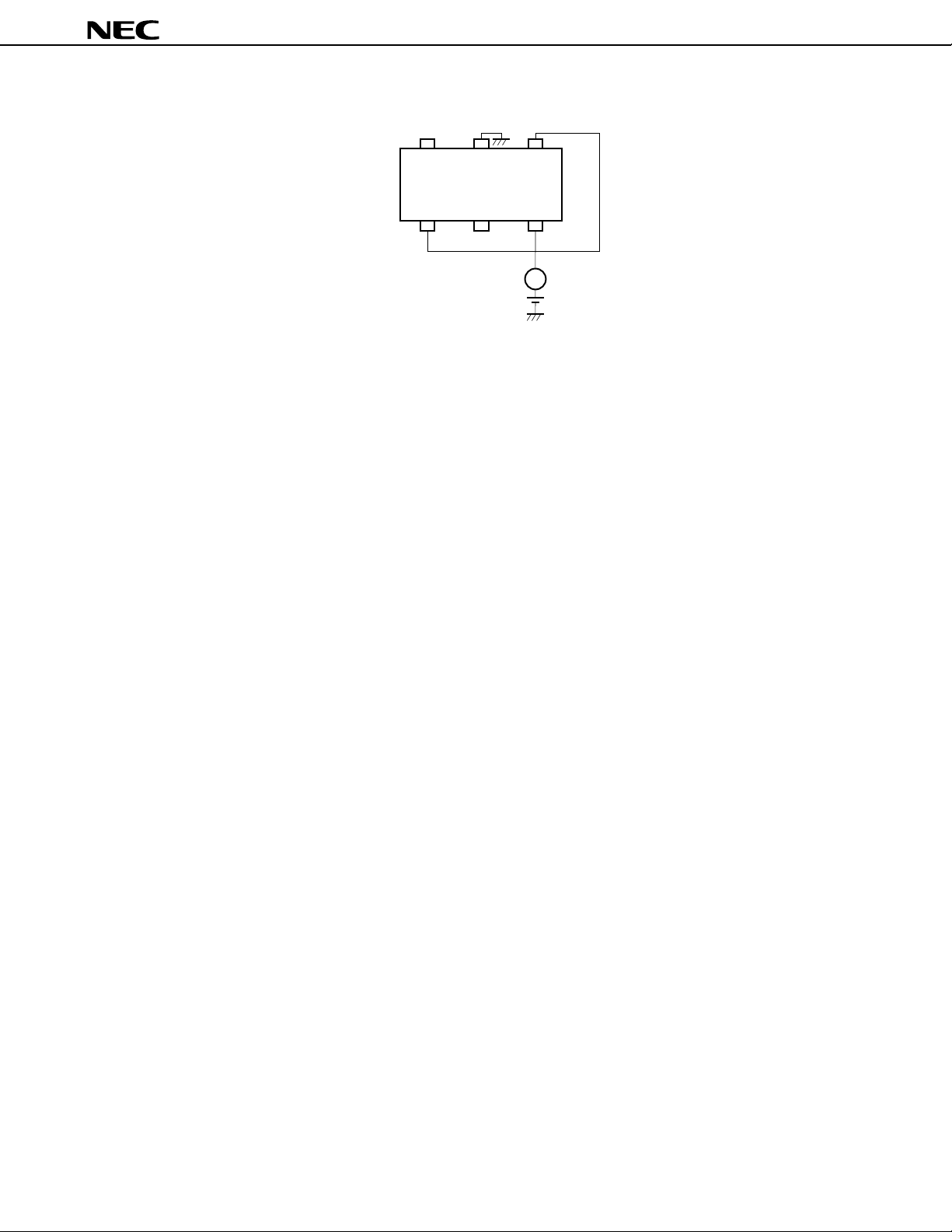
1: INPUT
2: GND
3: OUTPUT
4: V
CC
5: C1
6: C2
Document No. P11501EJ2V0DS00
(Previous No. ID-3534)
Date Published May 1996 P
Printed in Japan
Caution Electro-static sensitive devices
©
1996
Page 2
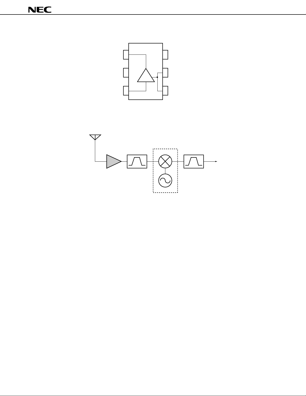
INTERNAL BLOCK DIAGRAM
µ
PC8102T
3
2
1
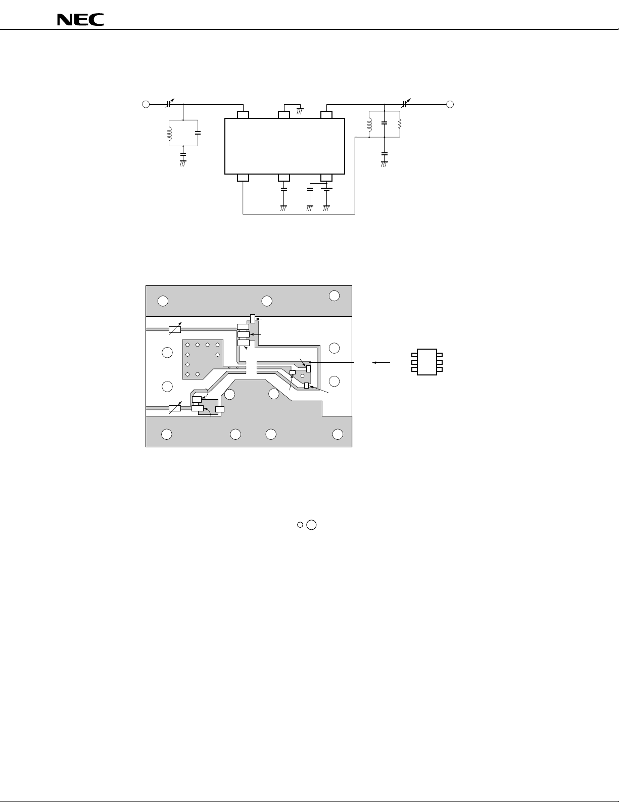
SYSTEM APPLICATION EXAMPLE AS PAGER
150 MHz to 330 MHz
µ
PC8102T BPF
µ
PC8103T
4
5
6
BPF
IF
2
Page 3
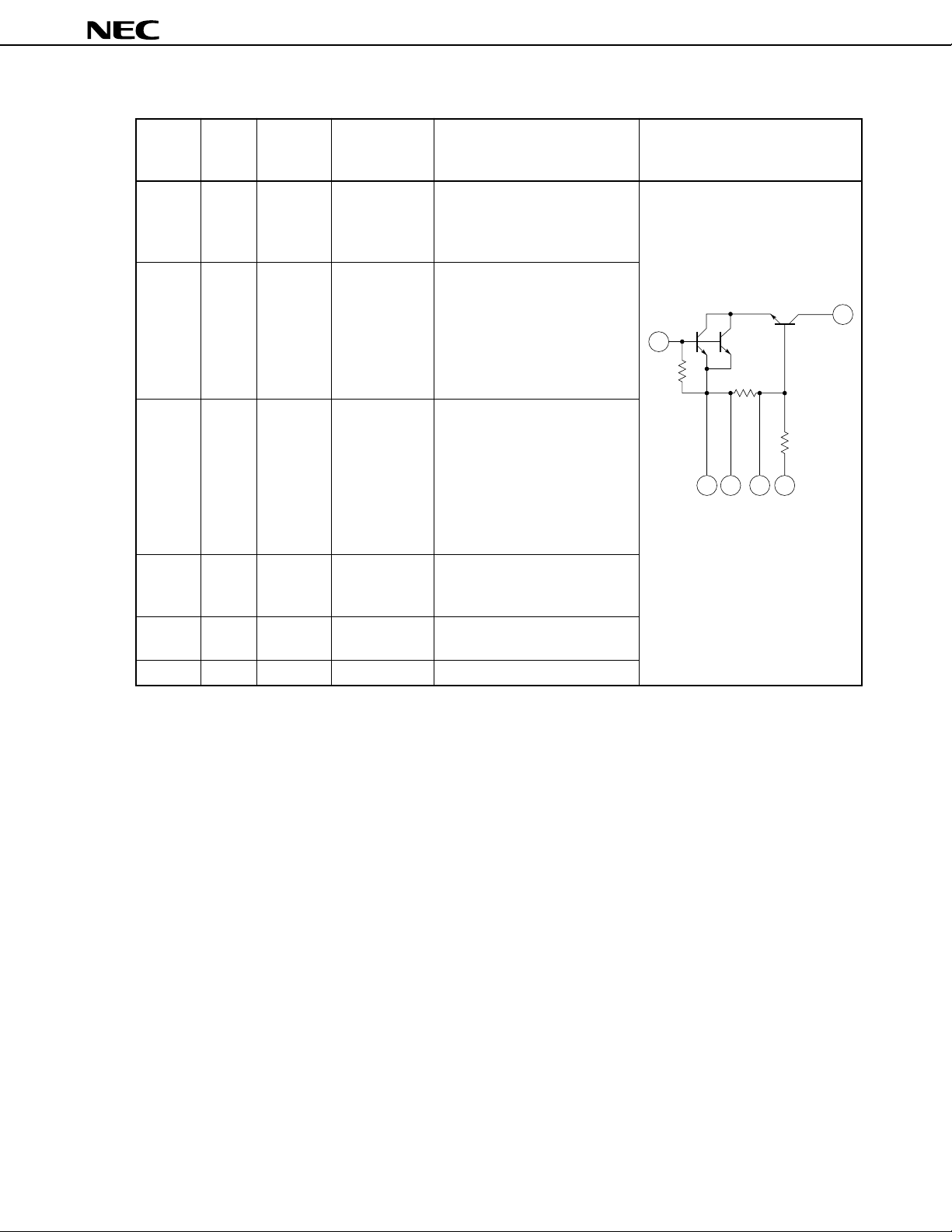
PIN EXPLANATION
1
26 54
3
µ
PC8102T
SUPPLY
PIN NO. NAME VOLTAGE
(V)
1 INPUT — 0.75 RF signal input pin. This pin
2 GND 0 — This ground pin must be
3 OUTPUT — Amplified signal output pin.
4VCC 0.9 to 2.0 — Supply voltage pin. Connect
5 C1 — 0.88 Ground with capacitance pin (eg
6 C2 — 0.85 AC ground pin for output
C2 pin
voltage
must be
applied
through
external
matching
inductor
PIN VOLTAGE
(V)
FUNCTION AND APPLICATION EQUIVALENT CIRCUIT
should be externally equipped
with matching circuit in accordance with desired frequency.
connected to the system ground
with minimum inductance.
Ground pattern on the board
should be formed as wide as
possible. Track length should
be kept as short as possible.
This pin should be externally
equipped with matching circuit
in accordance with desired
frequency.
bypass capacitor (eg 1000 pF)
to minimize ground impedance.
1000 pF).
Note Pin voltage values are described at VCC = 1 V.
3
Page 4
µ
PC8102T
ABSOLUTE MAXIMUM RATINGS
PARAMETER SYMBOL CONDITION RATINGS UNIT
Supply Voltage VCC TA = +25 ˚C 2.2 V
Power Dissipation PD Mounted on 50 × 50 × 1.6 mm double copper 280 mW
clad epoxy glass PWB at TA = +85 ˚C
Operating Temperature Topt –40 to +85 ˚C
Storage Temperature Tstg –55 to +150 ˚C
RECOMMENDED OPERATING CONDITIONS
PARAMETER SYMBOL MIN. TYP. MAX. UNIT
Supply Voltage VCC 0.9 1.0 2.0 V
Operating Temperature Topt –40 +25 +85 ˚C
Operating Frequency fopt 150 330 MHz
Electric characteristic (TA = +25 ˚C, VCC = 1.0 V, ZS = ZL = 50
PARAMETER SYMBOL TEST CONDITIONS
Circuit Current ICC No input signal, TEST CIRCUIT 1 0.30 0.5 0.65 mA
Power Gain GP f = 280 MHz, TEST CIRCUIT 3 10.0 13.5 16.5 dB
Output 3rd order OIP3 f1 = 150.000 MHz, f2 = 150.025 MHz — –5 — dBm
intercept point TEST CIRCUIT 2
ΩΩ
Ω)
ΩΩ
µ
PC8102T
MIN. TYP. MAX.
Note External matching circuits should be attached to input and output pins.
Standared characteristics for reference (Sample: I
PARAMETER SYMBOL CONDITIONS Reference value UNIT
matched with 50 Ω
Power Gain 1 GP1 f = 150 MHz, TEST CIRCUIT 2 20.6 dB
Noise Figure 1 NF1 3.6 dB
Power Gain 2 GP2 f = 280 MHz, TEST CIRCUIT 3 14.7 dB
Noise Figure 2 NF2 4.0 dB
Power Gain 3 GP3 f = 330 MHz, TEST CIRCUIT 5 14.5 dB
Noise Figure 3 NF3 4.1 dB
matched to optimize NF
Power Gain 4 GP4 f = 150 MHz, TEST CIRCUIT 2 19.4 dB
Noise Figure 4 NF4 2.3 dB
Power Gain 5 GP5 f = 280 MHz, TEST CIRCUIT 4 14.0 dB
Noise Figure 5 NF5 2.9 dB
Power Gain 6 GP6 f = 330 MHz, TEST CIRCUIT 6 11.6 dB
Noise Figure 6 NF6 3.1 dB
CC = 0.55 mA, Condition: TA = +25 ˚C, VCC = 1.0 V)
UNIT
4
Page 5
TEST CIRCUIT 1
123
IN GND OUT
µ
PC8102T
C2 C1 V
654
CC
A
5
Page 6
µ
PC8102T
TEST CIRCUIT 2 (150 MHz) <Matched with 50
(Note)
7.5 pF
68 nH
10 pF
1 000 pF
ΩΩ
Ω or matched to optimize NF>
ΩΩ
213
IN
C2
1 000 pF
GND OUT
CCC1
564
1 000
pF
V
84 nH
7.5 pF
10
47 kΩ
pF
1 000 pF
(Note)
Note Matching can be adjusted with trimmer condenser.
ILLUSTRATION OF THE TEST CIRCUIT 2 ASSEMBLED ON EVALUATION BOARD
47k
1 000 pF
84 nH
Ω
1 000 pF
1 000 pF
8102/07
1 000 pF
3
V
CC
2
C2B
1
Mounting direction
OUT
10 pF
7.5pF
10 pF
7.5pF
IN
1 000 pF
68 nH
4
5
6
Note
(*1) 35 × 42 × 0.4 mm double copper clad polyimide board
(*2) Back side: GND pattern
(*3) Solder plated on pattern
: Through holes
(*4)
6
Page 7

µ
C2B
3
2
1
4
5
6
1 000 pF
Mounting direction
1 000 pF
VCC
OUT
IN
PC8102/07
TYPE2
µ
PC8102T
IN
C2
1 000 pF
ΩΩ
Ω>
ΩΩ
213
GND OUT
C1
564
1 000
pF
23 nH
V
CC
2 pF
10
47 kΩ
pF
1 000 pF
TEST CIRCUIT 3 (280 MHz) <Matched with 50
0.5 pF
5 pF
23 nH
2 pF
0.5 pF
1 000 pF
ILLUSTRATION OF THE TEST CIRCUIT 3 ASSEMBLED ON EVALUATION BOARD
OUT
47 kΩ
1 000 pF
0.5 pF
2 pF
10 pF
23 nH
2 pF
0.5 pF
1 000 pF
23 nH
IN
5 pF
Note
(*1) 35 × 42 × 0.4 mm double copper clad polyimide board
(*2) Solder plated on pattern
: Through holes
(*3)
7
Page 8

TEST CIRCUIT 4 (280 MHz) <Matched to optimize NF>
27 nH
10 pF
IN
213
GND OUT
23 nH
10
pF
2 pF
47 kΩ
µ
PC8102T
2 pF
1 000 pF
C2
1 000 pF
V
C1
564
1 000
pF
CC
1 000 pF
ILLUSTRATION OF THE TEST CIRCUIT 4 ASSEMBLED ON EVALUATION BOARD
1 000 pF
1 000 pF
IN
µ
PC8102/07
TYPE2
OUT
VCC
3
2
1
C2B
Mounting direction
4
5
6
OUT
47 kΩ
1 000 pF
2 pF
10 pF
23 nH
2 pF
0.5 pF
1 000 pF
27 nH
IN
10 pF
Note
(*1) 35 × 42 × 0.4 mm double copper clad polyimide board
(*2) Solder plated on pattern
: Through holes
(*3)
8
Page 9

µ
C2B
3
2
1
4
5
6
1 000 pF
Mounting direction
1 000 pF
VCC
OUT
IN
PC8102/07
TYPE2
µ
PC8102T
IN
C2
1 000 pF
ΩΩ
Ω>
ΩΩ
213
GND OUT
564
1 000
pF
23 nH
VCCC1
1.5 pF
5
47 kΩ
pF
1 000 pF
TEST CIRCUIT 5 (330 MHz) <Matched with 50
6 pF
17 nH
3 pF
1 000 pF
ILLUSTRATION ON THE TEST CIRCUIT 5 ASSEMBLED ON EVALUATION BOARD
OUT
1.5 pF
47 kΩ
1 000 pF
6 pF
5 pF
23 nH
3 pF
1 000 pF
17 nH
IN
Note
(*1) 35 × 42 × 0.4 mm double copper clad polyimide board
(*2) Solder plated on pattern
: Through holes
(*3)
9
Page 10

TEST CIRCUIT 6 (330 MHz) <Matched to optimize NF>
µ
PC8102T
23 nH
10 pF
3 pF
1 000 pF
IN
C2
1 000 pF
213
GND OUT
C1
564
1 000
pF
23 nH
V
CC
2 pF
6
47 kΩ
pF
1 000 pF
ILLUSTRATION ON THE TEST CIRCUIT 6 ASSEMBLED ON EVALUATION BOARD
1 000 pF
1 000 pF
IN
µ
PC8102/07
TYPE2
OUT
VCC
3
2
1
C2B
Mounting direction
4
5
6
OUT
47 kΩ
1 000 pF
10 pF
2 pF
6 pF
23 nH
3 pF
1 000 pF
23 nH
IN
Note
(*1) 35 × 42 × 0.4 mm double copper clad polyimide board
(*2) Solder plated on pattern
: Through holes
(*3)
10
Page 11

CHARACTERISTICS (TA = +25 ˚C unless otherwise specified)
TA = +85˚C
TA = –40˚C
CIRCUIT CURRENT vs. SUPPLY VOLTAGE
5
4
3
2
1
0.5 1.0 1.5 2.0 2.5
0
V
CC
- SUPPLY VOLTAGE - V
I
CC
- CURCUIT CURRENT - mA
TA = +25˚C
– TEST CIRCUIT 1 –
µ
PC8102T
– TEST CIRCUIT 2 (matched with 50
ΩΩ
Ω) –
ΩΩ
150 MHz VCC = 1.0 V , ICC = 0.55 mA NF = 3.55 dB
CH1 S
11
C2
1 U FS 1: 54.377
MARKER 1
150 MHz
–5.166
Ω
205.30 nH
Ω
150.000 000 MHz
CH1 S
C2
12
log MAG 10 dB/ REF 0 dB 1: –41.406 dB
150.000 000 MHz
MARKER 1
150 MHz
1
1
CENTER 150.000 000 MHz SPAN 200.000 000 MHz
CH1
O21log MAG 10 dB/ REF 0 dB 1: 20.543 dB
C2
MARKER 1
150 MHz
150.000 000 MHz
1
CENTER 150.000 000 MHz SPAN 200.000 000 MHz
CH1 S
22
1 U FS 1: 47.934
C2
0.7613Ω826.93 pH
Ω
150.000 000 MHz
MARKER 1
150 MHz
1
CENTER 150.000 000 MHz
SPAN 200.000 000 MHz
CENTER 150.000 000 MHz SPAN 200.000 000 MHz
11
Page 12

– TEST CIRCUIT 2 (matched to optimize NF) –
150 MHz VCC = 1.0 V , ICC = 0.55 mA NF = 2.25 dB
11
CH1 S
1 U FS 1: 76.062
73.316
Ω
77.791 nH
Ω
150.000 000 MHz
CH1 S
12
log MAG 10 dB/ REF 0 dB 1: –43.251 dB
150.000 000 MHz
µ
PC8102T
C2
1
CENTER 150.000 000 MHz SPAN 200.000 000 MHz
CH1
S21log MAG 10 dB/ REF 0 dB 1: 19.418 dB
C2
150.000 000 MHz
1
C2
1
CENTER 150.000 000 MHz SPAN 200.000 000 MHz
22
CH1 S
C2
1 U FS 1: 53.445
– 1.0137Ω1.0467 nF
Ω
150.000 000 MHz
1
CENTER 150.000 000 MHz
SPAN 200.000 000 MHz
CENTER 150.000 000 MHz SPAN 200.000 000 MHz
12
Page 13

µ
PC8102T
– TEST CIRCUIT 3 (matched with 50
ΩΩ
Ω) –
ΩΩ
280 MHz VCC = 1.0 V , ICC = 0.55 mA NF = 4.0 dB
11 1 U FS 1: 84.699
CH1 S
C2
De1
–2.8789
Ω
197.44 pF
Ω
280.000 000 MHz
1
CENTER 280.000 000 MHz SPAN 200.000 000 MHz
CH1 S21 log MAG 10 dB/ REF 0 dB 1: 14.748 dB
280.000 000 MHz
C2
De1
1
CH1 S12 log MAG 10 dB/ REF 0 dB 1: –32.145 dB
C2
De1
260.000 000 MHz
1
CENTER 260.000 000 MHz SPAN 200.000 000 MHz
CH1 S
22 1 U FS 1: 51.172
C2
De1
4.5469
Ω
2.5845 nH
Ω
280.000 000 MHz
CENTER 280.000 000 MHz SPAN 200.000 000 MHz
1
CENTER 280.000 000 MHz SPAN 200.000 000 MHz
13
Page 14

– TEST CIRCUIT 4 (matched to optimize NF) –
µ
PC8102T
V
CC
75.09
280.000 000 MHz
CH1 S
C2
De1
11
1 U FS 1: 81.02
280 MHz
Ω
1
CENTER 280.000 000 MHz SPAN 200.000 000 MHz
21
CH1 S
C2
De1
log MAG 10 dB/ REF 0 dB 1: 14.087 dB
280.000 000 MHz
1
= 1.0 V , ICC = 0.55 mA
12
Ω
42.682 nH
CH1 S
C2
De1
CENTER 280.000 000 MHz SPAN 200.000 000 MHz
CH1 S
C2
De1
TA = 25 ˚C
log MAG 10 dB/ REF 0 dB 1: –33.561 dB
NF = 2.93 dB
280.000 000 MHz
1
22
1 U FS 1: 56.415
–6.4043Ω67.633 pF
Ω
280.000 000 MHz
1
CENTER 280.000 000 MHz SPAN 200.000 000 MHz
CENTER 280.000 000 MHz SPAN 200.000 000 MHz
14
Page 15

µ
PC8102T
– TEST CIRCUIT 5 (matched with 50
330 MHz
11
CH1 S
C2
De1
CH1 S
C2
De1
1 U FS 1: 57.111
CENTER 330.000 000 MHz SPAN 200.000 000 MHz
21
log MAG 10 dB/ REF 0 dB 1: 14.479 dB
11.426
Ω
1
1
ΩΩ
Ω) –
ΩΩ
V
CC
= 1.0 V , ICC = 0.55 mA
5.5105 nH
Ω
330.000 000 MHz
330.000 000 MHz
12
CH1 S
C2
CH1 S
C2
De1
log MAG 10 dB/ REF 0 dB 1: –30.38 dB
CENTER 330.000 000 MHz
22
1 U FS 1: 60.922
NF = 4.1 dB
1
SPAN 200.000 000 MHz
Ω
– 91.797Ω5.2539 nF
330.000 000 MHz
330.000 000 MHz
CENTER 330.000 000 MHz SPAN 200.000 000 MHz
1
CENTER 330.000 000 MHz SPAN 200.000 000 MHz
15
Page 16

– TEST CIRCUIT 6 (matched to optimize NF) –
330 MHz VCC = 1.00 V , ICC = 0.55 mA NF = 3.14 dB
11
CH1 S
1 U FS 1: 157.77
–17.273Ω27.921 pF
Ω
330.000 000 MHz
CH1 S
12
log MAG 10 dB/ REF 0 dB 1: –30.649 dB
330.000 000 MHz
µ
PC8102T
C2
De1
1
CENTER 330.000 000 MHz SPAN 200.000 000 MHz
21
CH1 S
C2
De1
log MAG 10 dB/ REF 0 dB 1: 11.58 dB
330.000 000 MHz
1
C2
De1
1
CENTER 330.000 000 MHz SPAN 200.000 000 MHz
22
CH1 S
C2
De1
1 U FS 1: 47.793
–6.7441Ω71.512 pF
Ω
330.000 000 MHz
1
CENTER 330.000 000 MHz SPAN 200.000 000 MHz
CENTER 330.000 000 MHz SPAN 200.000 000 MHz
16
Page 17

– TEST CIRCUIT 2 –
IM
+10
0
–10
3
AND OUTPUT LEVEL vs. INPUT LEVEL (150 MHz)
µ
PC8102T
(dBm)
3
3rd order intermodulation distortion IM
–20
P
–30
–40
Output level Pout [dBm]
–50
–60
–70
–80
–70 –60 –50 –40 –30 –20 –10
INPUT LEVEL Pin [dBm]
OUT
IM
3
17
Page 18

6 PIN MINI MOLD PACKAGE DIMENSIONS (Unit: mm)
µ
PC8102T
+0.2
2.8 –0.3
+0.2
123
1.5 –0.1
654
0.95 0.95
2.9 ±0.2
+0.1
0.3 –0.05
1.9
0.8
+0.2
1.1 –0.1
0.13 ±0.1
0 to 0.1
18
Page 19

µ
PC8102T
NOTE ON CORRECT USE
(1) Observe precautions for handling because of electro-static sensitive devices.
(2) Form a ground pattern as wide as possible to minimize ground impedance (to prevent undesired oscillation).
(3) Keep the track length of the ground pins as short as possible.
(4) The bypass capacitor (eg 1 000 pF) should be attached to the V
CC pin.
(5) The matching circuit must be each attached to input and output pins.
RECOMMENDED SOLDERING CONDITIONS
This product should be soldered in the following recommended conditions. Other soldering methods and conditions
than the recommended conditions are to be consulted with our sales representatives.
µ
PC8102T
Soldering process Soldering conditions
Infrared ray reflow Package peak temperature: 235 ˚C, IR35-00-3
Hour: within 30 s. (more than 210 ˚C),
Time: 3 time, Limited days: no.*
VPS Package peak temperature: 215 ˚C, VP15-00-3
Hour: within 40 s. (more than 200 ˚C),
Time: 3 time, Limited days: no.*
Wave Soldering Soldering tub temperature: less than 260 ˚C, Hour: within 10 s. WS60-00-1
Time: 1 time, Limited days: no.*
Pin part heating Pin area temperature: less than 300 ˚C, Hour: within 3 s/pin.
Limited days: no.*
Recommended condition
symbol
* It is the storage days after opening a dry pack, the storage conditions are 25 ˚C, less than 65 % RH.
Note The combined use of soldering method is to be avoided (However, except the pin area heating method).
For details of recommended soldering conditions for surface mounting, refer to information document SEMICON-
DUCTOR DEVICE MOUNTING TECHNOLOGY MANUAL (C10535EJ7V0IF00).
19
Page 20

µ
PC8102T
No part of this document may be copied or reproduced in any form or by any means without the prior written
consent of NEC Corporation. NEC Corporation assumes no responsibility for any errors which may appear in this
document.
NEC Corporation does not assume any liability for infringement of patents, copyrights or other intellectual
property rights of third parties by or arising from use of a device described herein or any other liability arising
from use of such device. No license, either express, implied or otherwise, is granted under any patents,
copyrights or other intellectual property rights of NEC Corporation or others.
While NEC Corporation has been making continuous effort to enhance the reliability of its semiconductor devices,
the possibility of defects cannot be eliminated entirely. To minimize risks of damage or injury to persons or
property arising from a defect in an NEC semiconductor device, customer must incorporate sufficient safety
measures in its design, such as redundancy, fire-containment, and anti-failure features.
NEC devices are classified into the following three quality grades:
“Standard“, “Special“, and “Specific“. The Specific quality grade applies only to devices developed based on
a customer designated “quality assurance program“ for a specific application. The recommended applications
of a device depend on its quality grade, as indicated below. Customers must check the quality grade of each
device before using it in a particular application.
Standard: Computers, office equipment, communications equipment, test and measurement equipment,
audio and visual equipment, home electronic appliances, machine tools, personal electronic
equipment and industrial robots
Special: Transportation equipment (automobiles, trains, ships, etc.), traffic control systems, anti-disaster
systems, anti-crime systems, safety equipment and medical equipment (not specifically designed
for life support)
Specific: Aircrafts, aerospace equipment, submersible repeaters, nuclear reactor control systems, life
support systems or medical equipment for life support, etc.
The quality grade of NEC devices in “Standard“ unless otherwise specified in NEC's Data Sheets or Data Books.
If customers intend to use NEC devices for applications other than those specified for Standard quality grade,
they should contact NEC Sales Representative in advance.
Anti-radioactive design is not implemented in this product.
20
M4 94.11
 Loading...