

Page 1
DATA SHEET
BIPOLAR NALOG NTEGRATED IRCUIT
PC2726T
µµµµ
1.6 GHz DIFFERENTIAL WIDE BAND AMPLIFIER
SILICON BIPOLAR MONOLITHIC INTEGRATED CIRCUIT
DESCRIPTION
The µPC2726T is a silicon microwave monolithic integrated circuit designed for miniature differenctial amplifier.
This IC operates up to 1.6 GHz and therefore is suitable for BS tuner, mobile communication and measurement
equipment applications. This IC can also use as differential oscillator application.
The µPC27×× series is manufactured using NEC’s 20 GHz fT NESATTM III silicon bipolar process. This process
uses silicon nitride passivation film and gold metallization wirings. These materials can protect the chips from
external pollution and prevent corrosion and migration. Thus, this process can produce the ICs with excellent
performance, uniformity and reliability.
FEATURES
• Wide frequency respone − fU= 1.6 GHz @ −3 dB GP, VCC = 5 V
• Power gain − GP = 15 dB @ 5 V
• Low power consumption: 5 V, 15 mA TYP./2 V, 2.5 mA
• 6 pin mini mold for high-density surface mounting.
ORDERING INFORMATION
PART NUMBER PACKAGE SUPPLYING FORM
µ
PC2726T-E3 6 pin mini mold Embossed tape 8 mm wide. 3 kp/reel.
Pin 1, 2, 3 face to perforation side of the tape.
For evaluation sample order, please contact your local NEC sales office. (Part number:
*
µ
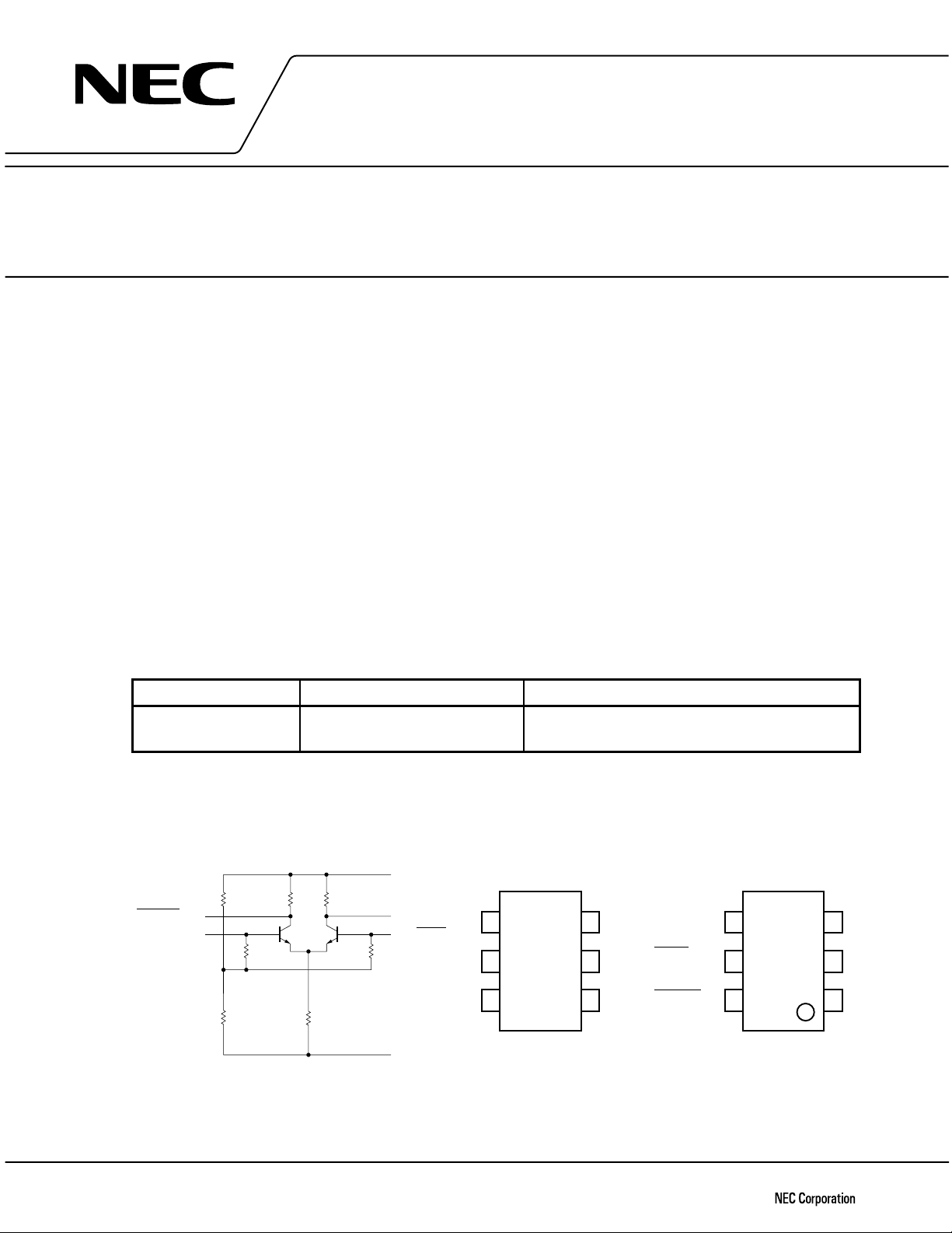
EQUIVALENT CIRCUIT PIN CONNECTIONS
VCC
RF OUT
RF IN
<4>
<6>
<5>
<3>
<1>
RF OUT
RF IN
3
2
1
(Top View)
C 1 P
4
5
6
1. INPUT
2. GND
3. OUTPUT
4. OUTPUT
5. V
CC
6. INPUT
4
5
6
PC2726T)
(Bottom View)
3
2
1
Document No. P10873EJ2V0DS00 (2nd edition)
(Previous No. IC-3125)
Date Published March 1997 N
Printed in Japan
GND<2>
Caution: Electro-static sensitive device
1994©
Page 2
ABSOLUTE MAXIMUM RATINGS
PPPP
PC2726T
Supply Voltage V
Power Dissipation of Package Allowance P
CC
6VT
D
280 mW Mounted on 50 u 50 u 1.6 mm
A
= +25 °C
epoxy glass
PWB at TA = +85 °C
opt
stg
in
40 to +85 °C
ð
55 to +150 °C
ð
0 dBm TA = +25 °C
Input Power P
Operating Temperature T
Storage Temperature T
RECOMMENDED OPERATING CONDITIONS
PARAMETERS SYMBOL MIN. TYP. MAX. UNIT
Supply Voltage V
Operating Temperature T
ELECTRICAL CHARACTERISTICS (TA = +25 °C, VCC = 5. V, ZL = ZS = 50
PARAMETERS SYMBOL MIN. TYP. MAX. UNIT TEST CONDITIONS
Circuit Current I
Power Gain G
Noise Figure NF 4.5 6.0 dB f = 400 MHz
Upper Limit Operating Frequency f
Isolation ISL 60 dB f = 400 MHz
Input Return Loss RL
Output Return Loss RL
Maximum Output Level P
CC
A
CC
P
U
out
O(sat)
4.5 5.0 5.5 V
ð40 +25 +85 °C
)
::::
8.0 11.5 15.0 mA No input signal
11.0 15 17.0 dB f = 400 MHz
1.0 1.6 GHz 3 dB down below flat gain at 0.4 GHz
in
2.0 dB f = 400 MHz
4.0 dB f = 400 MHz
ð5 ð2 dBm f = 400 MHz, Pin = ð10 dBm
STANDARD CHARACTERISTICS FOR REFERENCE (TA = +25 °C, ZL = ZS = 50
P
u
in
out
3
3
REFERENCE
VALUE
UNIT TEST CONDITIONS
2.5 mA VCC = 2 V, No input signal
4.5 dB VCC = 2 V, f = 400 MHz
2.4 GHz 3 dB down below flat gain at 0.4 GHz
1.0 dB VCC = 2 V, f = 400 MHz
4.0 dB VCC = 2 V, f = 400 MHz
ð14 dBm VCC = 2 V, f = 400 MHz, Pin = ð10 dBm
ð29 dBc VCC = 2 V, P
2
= 402 MHz
f
ð45 dBc VCC = 5 V, P
2
= 402 MHz
f
O(each)
= ð25 dBm, f1 = 400 MHz,
O(each)
= ð25 dBm, f1 = 400 MHz,
PARAMETERS SYMBOL
Circuit Current I
CC
Power Gain G
Noise Figure NF 5.1 dB VCC = 2 V, f = 400 MHz
Upper Limit Operating Frequency f
Isolation ISL 58 dB VCC = 2 V, f = 400 MHz
Input Return Loss RL
Output Return Loss RL
Maximum Output Power P
O(sat)
3rd Order Intermodulation Distortion IM
3rd Order Intermodulation Distortion IM
2
)
::::
Page 3
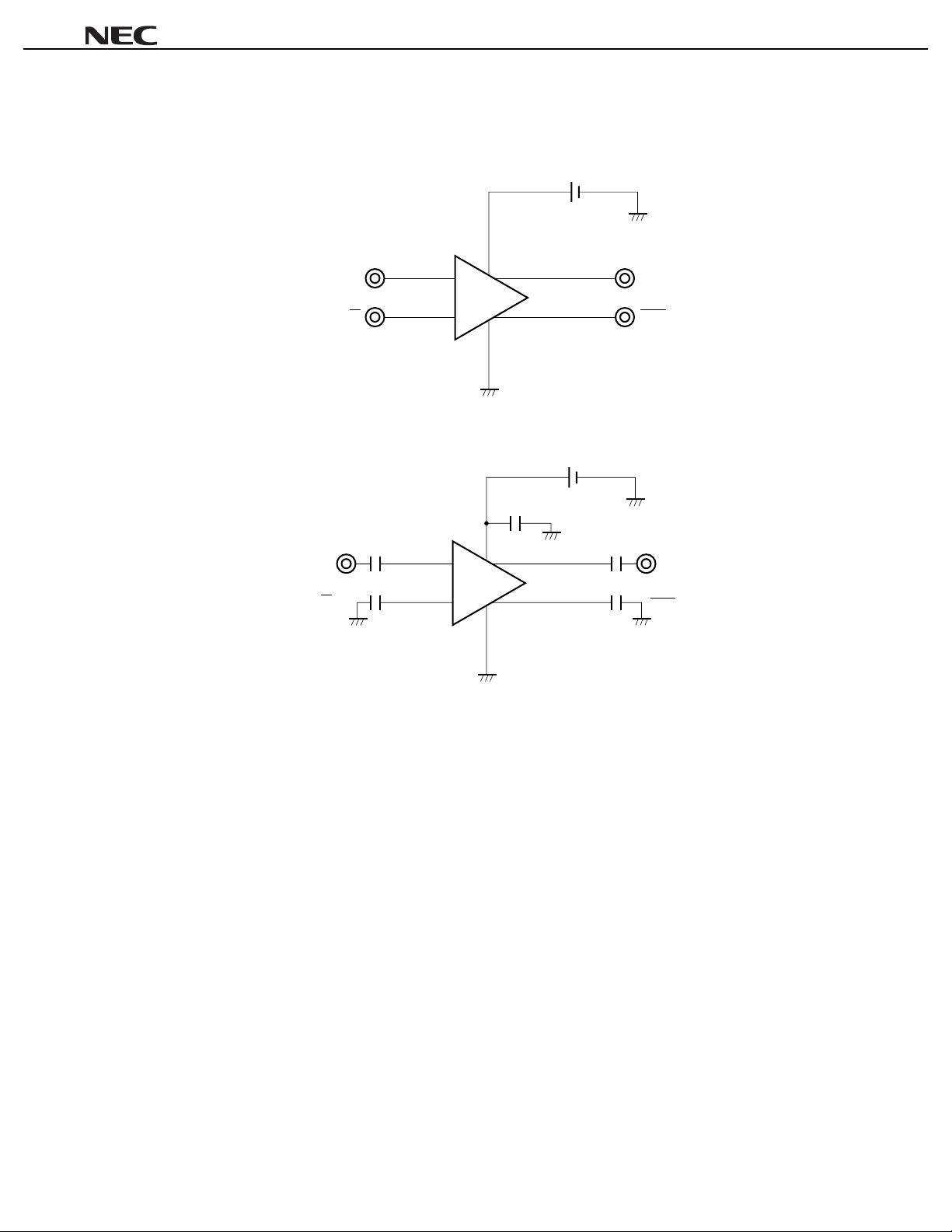
TEST CIRCUITS
DC Parameters
AC Parameters
V
CC
IN OUT
IN OUT
V
CC
5.0 V
5.0 V
PPPP
PC2726T
1 000 pF
CIN1 (1 000 pF)
IN OUT
IN
2 (1 000 pF)
C
IN
C
OUT
1 (1 000 pF)
OUT
2 (1 000 pF)
C
OUT
3
Page 4
PPPP
PC2726T
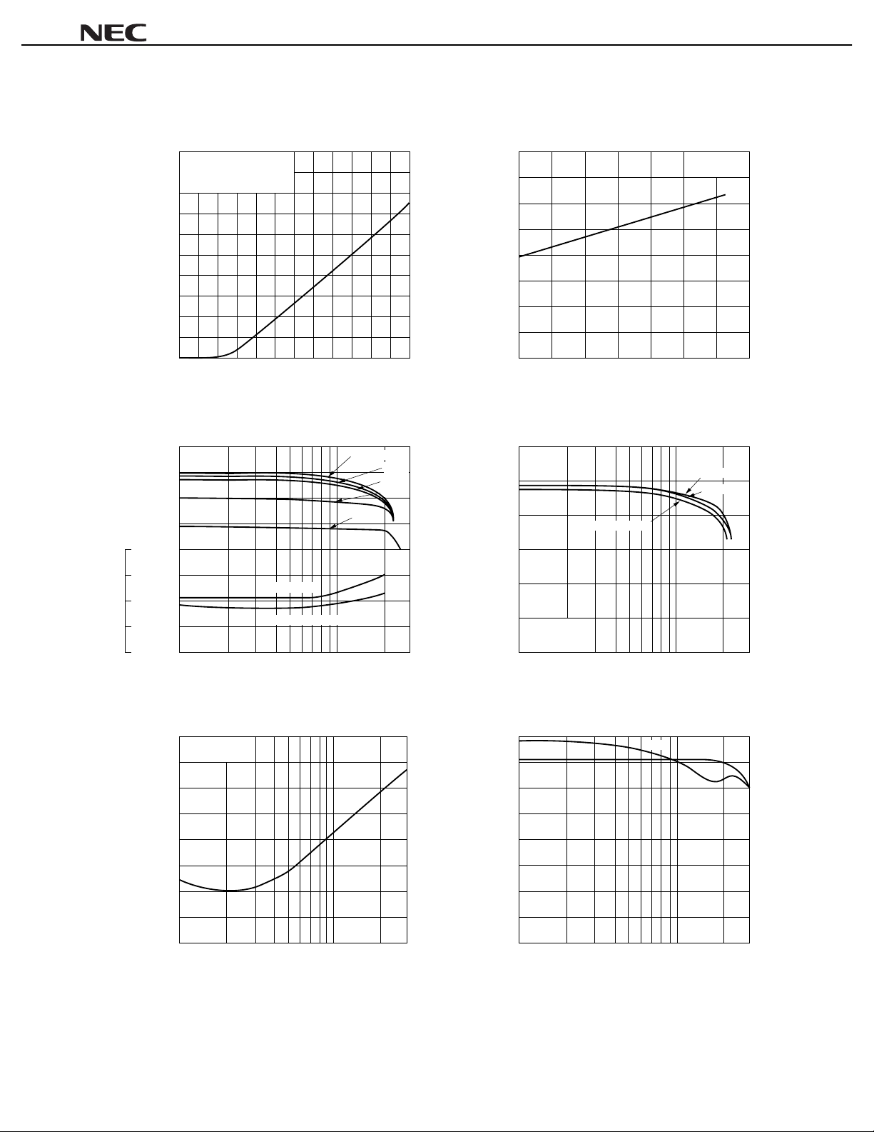
TYPICAL CHARACTERISTICS
CIRCUIT CURRENT vs. SUPPLY VOLTAGE
20
No input signals
18
16
14
12
10
8
6
– Circuit Current – mA
CC
I
4
2
– Power Gain – dB
P
G
9
02346
20
10
0
1
V
CC
– Supply Voltage – V
NOISE FIGURE, POWER GAIN vs.
FREQUENCY
P
G
(Unless otherwise specified T
5
VCC = 5.5 V
5.0 V
4.5 V
3.0 V
2.0 V
A
= +25 °C)
CIRCUIT CURRENT vs. OPERATING
TEMPERATURE
16
14
12
10
8
6
– Circuit Current – mA
4
CC
I
2
0
–20 20 60 100
opt
T
POWER GAIN vs. FREQUENCY
20
10
CC
V
0–40
40 80
– Operating Temperature – °C
VCC = +85 °C
= 5.0 V
–40 °C
+25 °C
7
NF
5
3
NF – Noise Figure – dB
1
0.1
0
VCC = 5.0 V
–20
–40
ISL – Isolation – dB
–60
–80
0.1
VCC = 2.0 V
VCC = 4.5 V - 5.5 V
0.3 1.0 3.0
f – Frequency – GHz
ISOLATION vs. FREQUENCY
0.3 1.0 3.0
f – Frequency – GHz
2.0
2.0
0
– Power Gain – dB
P
G
VCC = 5.0 V
–5
f – Frequency – GHz
RETURN LOSS vs. FREQUENCY
0
RL
out
–10
–20
– Output Return Loss – dB
–30
– Input Return Loss – dB
in
out
RL
RL
–40
0.1
f – Frequency – GHz
RL
RL
2.00.1
out
in
0.3 1.0 3.0
RL
in
0.3 1.0 2.0
4
Page 5

PPPP
PC2726T
10
f = 400 MHz
0
VCC = 5.5 V
VCC = 5.0 V
–10
–20
OUTPUT POWER vs. INPUT POWER
– Output Power – dBm
O
P
–30
–40
–50
–40 –30 –20
P
in
– Input Power – dBm
OUTPUT POWER vs. INPUT POWER
10
f = 1 GHz
0
VCC = 5.5 V
VCC = 5.0 V
VCC = 4.5 V
VCC = 2.0 V
–10
10
OUTPUT POWER vs. INPUT POWER
CC
= 5.0 V
0
–10
V
f = 400 MHz
T
A = +85 °C
T
A = +25 °C
TA = –40 °C
–20
– Output Power – dBm
O
P
–30
–40
0
–50
–40 –30 –20
P
in
– Input Power – dBm
–10
0
OUTPUT POWER vs. INPUT POWER
10
CC
= 5.0 V
V
0
–10
–20
– Output Power – dBm
O
P
–30
–40
–50
–40 –30 –20
P
in
– Input Power – dBm
SATURATED OUTPUT POWER vs.
FREQUENCY
0
–2
–4
VCC = 5.5 V
VCC = 5.0 V
–6
VCC = 4.5 V
–8
–10
–12
VCC = 2.0 V
–14
–16
– Saturated Output Power – dBm
O(sat)
–18
P
–20
0.1
0.2 3
0.5 1
f – Frequency – GHz
VCC = 4.5 V
VCC = 2.0 V
–10
–10
f = 400 MHz
–20
– Output Power – dBm
O
P
–30
f = 1 GHz
–40
0
–50
–40 –30 –20
P
in
– Input Power – dBm
–10
0
3rd ORDER INTERMODULATION DISTORTION
vs. OUTPUT POWER OF EACH TONE
60
f1 = 400 MHz
f
2
= 402 MHz
50
VCC = 5.5 V
VCC = 5.0 V
40
VCC = 4.5 V
30
VCC = 2.0 V
20
– 3rd Order Intermodulation Distortion – dBc
3
10
IM
2
–40 –20 –10
–30 0
P
O(each)
– Output Power of Each Tone – dBm
5
Page 6

S PARAMETER
S11-FREQUENCY
PPPP
PC2726T
0.13
0.12
0.11
0.39
100
0.9
0.8
0.7
0.5
0.6
0.7
0.8
REACTANCE COMPONENT
R
––––
(
)
Z
O
0.8
0.9
–110
–100
0.10
0.11
0.40
0.39
0.38
0.10
0.40
0.09
0.41
0.08
0.07
0.43
130
0.06
0.44
–150
0.05
O
140
P
0.4
M
CO
E
C
N
A
T
)
0.3
C
A
O
E
+JX
R
––––
(
E
V
Z
I
T
I
OS
P
0.1
0.2
T
N
E
N
O
P
)
OM
O
C
E
0.3
C
(
– JX
N
––––
A
T
C
A
E
R
0.4
–140
0.06
0.44
–130
000.07
0.43
0.05
0.45
R
O
T
A
R
0.04
E
0.46
150
N
E
G
D
R
0.03
A
S
0.47
E
W
0.2
E
O
R
T
G
S
E
H
D
T
0.02
G
0.48
N
I
N
T
E
N
L
0.1
E
E
I
V
C
A
F
0.01
0.49
W
F
E
O
C
0
N
0
0
O
I
T
C
E
L
F
E
R
0.01
0.1
0.49
F
O
E
L
G
N
0.02
A
0.48
0.2
–160
0.03
0.47
0.04
0.46
0.45
110
0.42
120
0.6
0.5
T
N
E
N
0.3
0.4
Z
IVE
T
A
G
NE
0.5
0.6
0.7
–120
0.08
0.42
0.09
0.41
0.14
0.37
90
1.0
0.2
0.4
0.2
0.9
1.0
0.2
0.4
0.2
1.0
–90
0.12
0.38
0.15
0.36
80
0.2
0.6
0.8
1.0
0.8
0.6
0.4
1.2
1.4
0.6
0.8
1.0
0.8
0.6
0.4
1.2
0.13
0.37
0.16
0.35
0.34
0.15
–70
0.35
0.17
0.33
0.18
0060
1.6
0.32
1.8
3.0
1.8
–60
1.6
0.16
0.34
0.19
50
0.31
2.0
4.0
2.0
0.17
0.33
0.20
40
0.30
0.21
3.0
0.29
30
0.22
4.0
0.28
20
6.0
0.23
0.27
10
10
0.24
0.26
20
50
0.25
0.25
0
20
10
5.0
–50
400 M
3.0
0.18
0.32
–40
0.19
50
100 M
6.0
4.0
–30
0.20
0.30
0.31
10
–20
50
20
–10
0.22
000.21
0.29
0.23
0.24
0.28
0.26
0.27
70
1.4
1.0
1.6
1.8
2.0
1 G
1.0
1.4
–80
0.04
0.36
S22-FREQUENCY
0.13
0.12
0.11
0.10
0.40
0.09
0.41
0.42
N
O
(
Z
IVE
T
0.5
–130
110
120
0.6
0.5
T
N
E
0.3
0.4
A
G
NE
0.6
0.7
–120
0.08
0.42
0.09
0.41
0.08
0.07
0.43
130
0.06
0.44
0.05
140
P
0.4
M
0.45
R
O
T
A
R
0.04
E
0.46
N
E
G
D
R
0.03
A
S
0.47
E
W
E
O
R
T
G
S
E
H
D
T
0.02
G
0.48
N
I
N
T
E
N
L
0.1
E
E
I
V
C
A
F
0.01
0.49
W
F
E
O
C
0
N
0
0
O
I
T
C
E
L
F
E
R
0.01
0.1
0.49
F
O
E
L
G
N
0.02
A
0.48
–160
0.03
0.47
0.04
0.46
CO
E
C
N
A
T
)
0.3
C
150
A
O
E
+JX
R
––––
(
E
V
Z
I
T
I
OS
P
0.2
0.1
0.2
T
0.2
N
E
N
O
P
)
OM
O
C
E
0.3
C
– JX
N
––––
–150
A
T
C
A
E
R
0.4
0.05
–140
0.45
0.06
0.44
000.07
0.43
0.38
0.39
100
0.9
0.8
0.7
0.5
0.6
0.7
0.8
REACTANCE COMPONENT
R
––––
(
)
Z
O
0.8
0.9
–110
–100
0.10
0.11
0.40
0.39
0.14
0.37
90
1.0
0.2
0.4
0.2
0.9
1.0
0.2
0.4
0.2
1.0
–90
0.12
0.38
0.15
0.36
80
0.2
0.6
0.8
1.0
0.8
0.6
0.4
1.2
1.4
0.6
0.8
1.0
0.8
0.6
0.4
1.2
0.13
0.37
0.16
0.35
0.34
0.15
–70
0.35
0.17
0.33
0.18
0060
1.6
0.32
2.0
4.0
100 M
400 M
1 G
2.0
0.17
50
0.33
0.19
0.31
0.20
40
0.30
0.21
3.0
0.29
30
0.22
4.0
0.28
20
6.0
0.23
0.27
10
10
0.24
0.26
20
50
0.25
0.25
0
20
10
5.0
50
50
0.24
0.26
20
–10
10
0.23
0.27
–20
0.22
6.0
0.28
4.0
000.21
–30
0.29
3.0
0.20
–40
0.30
0.19
0.31
–50
0.18
0.32
1.8
3.0
1.8
–60
1.6
0.16
0.34
70
1.4
1.0
1.6
1.8
2.0
1.0
1.4
–80
0.04
0.36
6
Page 7

ILLUSTRATION OF THE EVALUATION BOARD FOR TEST CIRCUIT
3.5 7 14 14
4 5.5 16.5 11
710411
16- 2.3
23 7.2 3
10.2
(8.8)
1.21.2 1
φφ
9- 0.8
PPPP
PC2726T
0.74
23 (6)
6
2.03
142.23°
0.29
51 3.8 11.2 5
4
0.74
9
12
7.23°
18.9
3.51
±0.02
2.06
±0.02
0.74
8
2
3.5
2.03
2.03
22
2.03
1.8
7.23
1
11
20.24
4
12.5 11.5 9
14 7 14
11.8
1.2
135°
22
2.03
8.24
1.52
42
1
1.8
2.03
2.03
±0.02
2.06
±0.02
2.06
±0.02
0.74
2.4
5.44
±0.02
18.16
9
35
14
Note
135°
1.51222
2.03(4.83)
2
2
22
2
7.28°
(1) 50 × 50 × 0.5 mm double copper clad polyimide board.
(2) Back side: GND pattern
(3) Solder plated on pattern
(4) : Through holes
45°
DETAIL LAYOUT t = 0.4
2.03
7
Page 8

EXAMPLE FOR SYSTEM APPLICATION
DBS tuner
< From ODU. >
PPPP
PC2726T
DETDC AMP
IF amp.
MIX.ATT RF amp.RF amp.1st IF input
Sound
Visual
µ
PC2723TµPC2726T FM DEMO
VCO
PLL
OP
LPF
8
Page 9

6 PINS MINI MOLD PACKAGE DIMENSIONS (Unit: mm)
+0.1
0.3
–0.05
123
–0.3
–0.1
+0.2
+0.2
1.5
2.8
65
4
0.13±0.1
0 to 0.1
PPPP
PC2726T
0.950.95
1.9
2.9±0.2
1.1
0.8
+0.2
–0.1
9
Page 10

PPPP
PC2726T
NOTE ON CORRECT USE
(1) Observe precautions for handling because of electro-static sensitive devices.
(2) Form a ground pattern as wide as possible to prevent an increase in ground impedance (which can cause
undesired oscillation).
(3) Keep the wiring length of the ground pins as short as possible.
(4) Connect a bypass capacitor (having, for example, a capacitance of 1 000 pF) to the VCC pin.
RECOMMENDED SOLDERING CONDITIONS
This product should be soldered in the following recommended conditions. Other soldering methods and
conditions than the recommended conditions are to be consulted with our sales representatives.
PC2726T
P
Soldering process Soldering conditions
Infrared ray reflow Package peak temperature: 235 °C,
Hour: within 30 s. (more than 210 °C),
Time: 3 times, Limited days; no.*
VPS Package peak temperature: 215 °C,
Hour: within 40 s. (more than 200 °C),
Time: 3 times, Limited days: no.*
Wave soldering Soldering tub temperature: less than 260 °C,
Hour: within 10 s.
Time: 1 time, Limited days: no.
Pin part heating Pin area temperature: less than 300 °C,
Hour: within 3 s.
Limited days: no.*
: It is the storage days after opening a dry pack, the storage conditions are 25 °C, less than 65 % RH.
*
Note 1.
The combined use of soldering method is to be avoided (However, except the pin area heating method).
Recommended condition
symbols
IR35-00-3
VP15-00-3
WS60-00-1
For details of recommended soldering conditions for surface mounting, refer to information document
SEMICONDUCTOR DEVICE MOUNTING TECHNOLOGY MANUAL (C10535E).
10
Page 11

[MEMO]
PPPP
PC2726T
11
Page 12

PPPP
PC2726T
The applicatoin circuit and circuit constants shown in this document are for reference only and may not be
employed for mass production of the application system.
No part of this document may be copied or reproduced in any form or by any means without the prior written
consent of NEC Corporation. NEC Corporation assumes no responsibility for any errors which may appear in this
document.
NEC Corporation does not assume any liability for infringement of patents, copyrights or other intellectual
property rights of third parties by or arising from use of a device described herein or any other liability arising
from use of such device. No license, either express, implied or otherwise, is granted under any patents,
copyrights or other intellectual property rights of NEC Corporation or others.
While NEC Corporation has been making continuous effort to enhance the reliability of its semiconductor devices,
the possibility of defects cannot be eliminated entirely. To minimize risks of damage or injury to persons or
property arising from a defect in an NEC semiconductor device, customers must incorporate sufficient safety
measures in its design, such as redundancy, fire-containment, and anti-failure features.
NEC devices are classified into the following three quality grades:
"Standard", "Special", and "Specific". The Specific quality grade applies only to devices developed based on
a customer designated "quality assurance program" for a specific application. The recommended applications
of a device depend on its quality grade, as indicated below. Customers must check the quality grade of each
device before using it in a particular application.
Standard: Computers, office equipment, communications equipment, test and measurement equipment,
audio and visual equipment, home electronic appliances, machine tools, personal electronic
equipment and industrial robots
Special: Transportation equipment (automobiles, trains, ships, etc.), traffic control systems, anti-disaster
systems, anti-crime systems, safety equipment and medical equipment (not specifically designed
for life support)
Specific: Aircrafts, aerospace equipment, submersible repeaters, nuclear reactor control systems, life
support systems or medical equipment for life support, etc.
The quality grade of NEC devices is "Standard" unless otherwise specified in NEC's Data Sheets or Data Books.
If customers intend to use NEC devices for applications other than those specified for Standard quality grade,
they should contact an NEC sales representative in advance.
Anti-radioactive design is not implemented in this product.
NESAT (NEC Silicon Advanced Technology) is a trademark of NEC Corporation.
M4 96. 5
 Loading...