

Page 1
Designed to reduce logic supply current, chip size, and system
cost, the UCN5833A/EP integrated circuits offer high-speed operation
for thermal printers. These devices can also be used to drive multiplexed LED displays or incandescent lamps within their 125 mA peak
output current rating. The combination of bipolar and MOS technologies gives BiMOS II smart power ICs an interface flexibility beyond the
reach of standard buffers and power driver circuits.
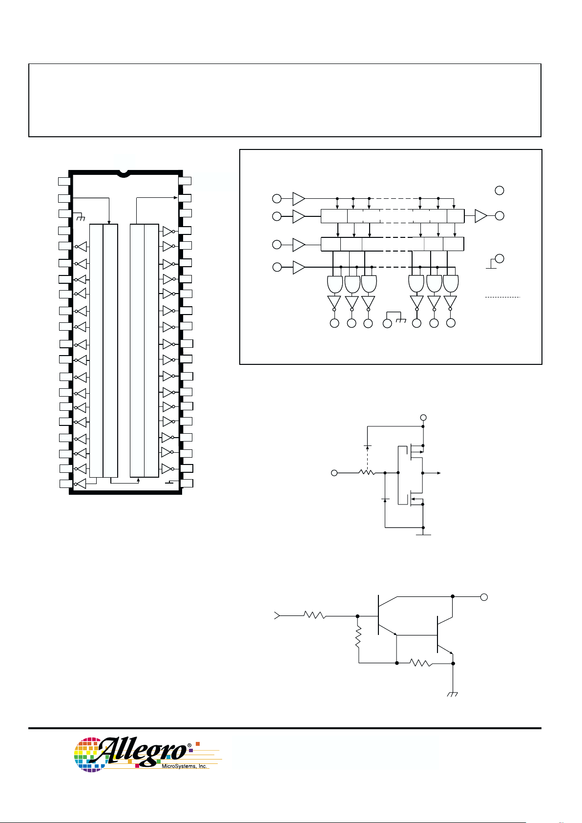
These 32-bit drivers have bipolar open-collector npn Darlington
outputs, a CMOS data latch for each of the drivers, a 32-bit CMOS
shift register, and CMOS control circuitry. The high-speed CMOS shift
registers and latches allow operation with most microprocessor-based
systems at data input rates above 3.3 MHz. Use of these drivers with
TTL may require input pull-up resistors to ensure an input logic high.
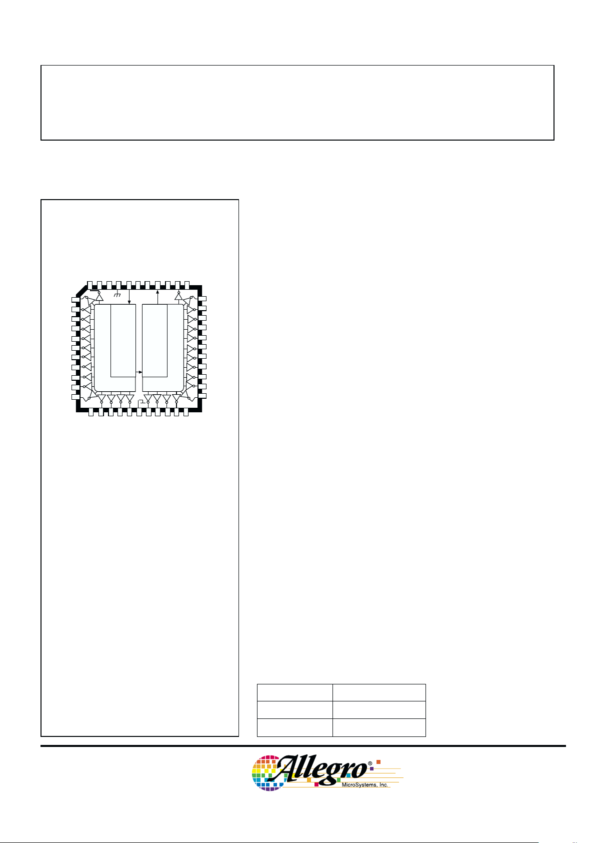
The UCN5833A is supplied in a 40-pin dual in-line plastic package
with 0.600" (15.24 mm) row spacing. At an ambient temperature of
+75°C, all outputs of the DlP-packaged device will sustain 50 mA
continuously. For high-density applications, the UCN5833EP is
available. This 44-lead plastic chip carrier (quad pack) is intended
for surface-mounting on solder lands with 0.050" (1.27 mm) centers.
CMOS serial data outputs permit cascading for applications requiring
additional drive lines.
FEATURES
■ To 3.3 MHz Data Input Rate
■ 30 V Minimum Output Breakdown
■ Darlington Current-Sink Outputs
■ Low-Power CMOS Logic and Latches
BiMOS II 32-BIT SERIAL-INPUT,
LATCHED DRIVER
UCN5833EP
ABSOLUTE MAXIMUM RATINGS
at +25°C Free-Air Temperature
Output Voltage, V
OUT
. . . . . . . . . . . 30 V
Logic Supply Voltage, V
DD
. . . . . . . 7.0 V
Input Voltage Range,
V
IN
. . . . . . . . . -0.3 V to V
DD
+ 0.3 V
Continuous Output Current,
l
OUT
(each output) . . . . . . . . . . 125 mA
Package Power Dissipation, P
D
(UCN5833A) . . . . . . . . . . . . . . . 3.5 W*
(UCN5833EP) . . . . . . . . . . . . . . 2.5 W*
Operating Temperature Range,
T
A
. . . . . . . . . . . . . . - 20°C to +85°C
Storage Temperature Range,
T
S
. . . . . . . . . . . . . -55°C to +150°C
* Derate linearly to 0 W at +150°C.
Caution: CMOS devices have input static protection
but are susceptible to damage when exposed to
extremely high static electrical charges.
Always order by complete part number:
Part Number Package
UCN5833A 40-Pin DIP
UCN5833EP 44-Lead PLCC
Dwg. No. A-13,049
1
4
5
6
18
1920212223
24
252627
28
40
41
42
43
44
2
3
7
8
9
10
11
12
13
14
15
16
17
OUT
2
OUT
3
OUT
4
OUT
5
OUT
6
OUT
7
OUT
8
OUT
9
OUT
OUT
10
OUT
11
12
OUTNCSTROBE1POWER GROUND
SERIAL DATA IN
LOGIC
SUPPLY
CLOCK
SERIAL DATA OUT
OUTPUT ENABLENCOUT
32
38
39
37
36
35
34
33
32
31
30
29
OUT
31
OUT
30
OUT
29
OUT
28
OUT
27
OUT
26
OUT
25
OUT
24
OUT
23
OUT
22
OUT
21
NC
OUT
13
OUT
14
OUT
15
OUT
16
LOGIC GROUND
OUT
17
OUT18OUT
19
OUT
20
NC
SUB
REGISTER
REGISTER
LATCHES
LATCHES
ST
CLK
OE
V
DD
Data Sheet
26185.16A*
5833
Page 2
5833
BiMOS II 32-BIT
SERIAL-INPUT,
LATCHED DRIVER
115 Northeast Cutoff, Box 15036
Worcester, Massachusetts 01615-0036 (508) 853-5000
V
CLK
DD
SERIAL
DATA I N
POWER
GROUND
STROBE
OUT
OUT
OUT
OUT
OUT
OUT
1
2
3
4
5
6
OUT
7
OUT
8
OUT
9
OUT
10
OUT
11
OUT
12
OUT
13
OUT
14
OUT
18
OUT
19
OUT
20
OUT
21
OUT
22
OUT
23
OUT
24
OUT
25
OUT
26
OUT
27
OUT
28
OUT
29
OUT
30
OUT
31
OUT
32
OUTPUT
ENABLE
LOGIC
SUPPLY
SERIAL
DATA O U T
LOGIC
GROUND
SUB
LOGIC
SUPPLY
40
39
38
37
34
35
36
31
32
33
30
22
29
28
27
26
25
24
23
21
1
2
3
4
7
6
5
10
9
8
11
12
12
14
15
16
17
18
19
20
ST
OUT
15
OUT
16
OUT
17
LATCHES
REGISTER
REGISTER
LATCHES
OE
Dwg. No. A-13,057
TYPICAL INPUT CIRCUIT
FUNCTIONAL BLOCK DIAGRAM
Dwg. No. A-13,048
Dwg. No. A-13,051
Dwg. No. A-13,050
TYPICAL OUTPUT DRIVER
UCN5833A
32-BIT SHIFT REGISTER
LATCHES
CLOCK
SERIAL
DATA I N
STROBE
OUTPUT
ENABLE
LOGIC
GROUND
V
DD
SERIAL DATA
OUT
SUB
MOS
BIPOLAR
OUT
OUT
OUT
OUT
OUT OUT
1
2
3
30
31
32
POWER
GROUND
IN
SUB
V
DD
OUT
115 Northeast Cutoff, Box 15036
Worcester, Massachusetts 01615-0036 (508) 853-5000
Copyright © 1986, 1995, Allegro MicroSystems, Inc.
CLOCK
Page 3
5833
BiMOS II 32-BIT
SERIAL-INPUT,
LATCHED DRIVER
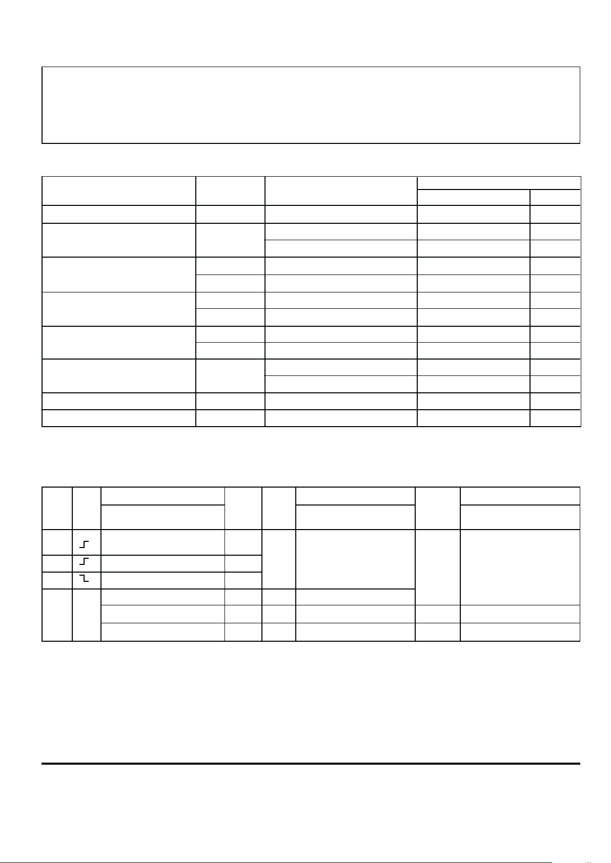
TRUTH TABLE
Serial Shift Register Contents Serial Latch Contents Output Output Contents
Data Clock Data Strobe Enable
Input Input I
1I2I3
... I
N-1IN
Output Input I1I2I3... I
N-1IN
Input I1I2I3... I
N-1
I
N
HHR
1R2
... R
N-2RN-1
R
N-1
LLR
1R2
... R
N-2RN-1
R
N-1
XR
1R2R3
... R
N-1RN
R
N
XXX...X X X L R1R2R3... R
N-1 RN
P1P2P3... P
N-1PN
P
N
HP1P2P3... P
N-1 PN
HP1P2P3... P
N-1
P
N
X X X ... X X L H H H ... H H
L = Low Logic Level H = High Logic Level X = Irrelevant P = Present State R = Previous State
ELECTRICAL CHARACTERISTICS at TA = +25°C, VDD = 5 V (unless otherwise noted).
Limits
Characteristic Symbol Test Conditions Min. Max. Units
Output Leakage Current I
CEX
V
OUT
= 30 V, TA = 70°C—10µA
Collector-Emitter V
CE(SAT)
l
OUT
= 50 mA — 1.2 V
l
OUT
= 100 mA — 1.7 V
Input Voltage V
IN(1)
3.5 5.3 V
V
IN(0)
-0.3 +0.8 V
Input Current l
IN(1)
VIN = 5.0 V — 1.0 µA
l
IN(0)
VIN = 0 V — -1.0 µA
Serial Output Voltage V
OUT(1)
I
OUT
= -200 µA 4.5 — V
V
OUT(0)
I
OUT
= 200 µA — 0.3 V
Supply Current l
DD
One output ON, l
OUT
= 100 mA — 1.0 mA
All outputs OFF — 50 µA
Output Rise Time t
r
l
OUT
= 100 mA, 10% to 90% — 500 ns
Output Fall Time t
f
l
OUT
= 100 mA, 90% to 10% — 500 ns
NOTE: Positive (negative) current is defined as going into (coming out of) the specified device pin.
Saturation Voltage
Page 4

5833
BiMOS II 32-BIT
SERIAL-INPUT,
LATCHED DRIVER
115 Northeast Cutoff, Box 15036
Worcester, Massachusetts 01615-0036 (508) 853-5000
TIMING CONDITIONS
(VDD = 5.0 V, Logic Levels are VDD and Ground)
A. Minimum Data Active Time Before Clock Pulse
(Data Set-Up Time) .......................................................................... 75 ns
B. Minimum Data Active Time After Clock Pulse
(Data Hold Time) ............................................................................. 75 ns
C. Minimum Data Pulse Width ................................................................ 150 ns
D. Minimum Clock Pulse Width ............................................................... 150 ns
E. Minimum Time Between Clock Activation and Strobe ....................... 300 ns
F. Minimum Strobe Pulse Width ............................................................. 100 ns
G. Typical Time Between Strobe Activation and
Output Transition ........................................................................... 500 ns
Dwg. No. A-12,276A
Serial Data present at the input is transferred to the shift register
on the logic “0” to logic “1” transition of the CLOCK input pulse. On
succeeding CLOCK pulses, the registers shift data information towards
the SERIAL DATA OUTPUT. The SERIAL DATA must appear at the
input prior to the rising edge of the CLOCK input waveform.
Information present at any register is transferred to its respective
latch when the STROBE is high (serial-to-parallel conversion). The
latches will continue to accept new data as long as the STROBE is
held high. Applications where the latches are bypassed (STROBE tied
high) will require that the OUTPUT ENABLE input be low during serial
data entry.
When the OUTPUT ENABLE input is low, all of the output buffers
are disabled (OFF) without affecting the information stored in the
latches or shift register. With the OUTPUT ENABLE input high, the
outputs are controlled by the state of the latches.
E F
CLOCK
DATA IN
STROBE
N
A D
B
C
G
OUTPUT
ENABLE
OUT
Page 5

5833
BiMOS II 32-BIT
SERIAL-INPUT,
LATCHED DRIVER
NOTES: 1. Exact body and lead configuration at vendor’s option within limits shown.
2. Lead spacing tolerance is non-cumulative.
3. Lead thickness is measured at seating plane or below.
UCN5833A
Dimensions in Inches
(controlling dimensions)
Dimensions in Millimeters
(for reference only)
40
14.73
12.32
1 2
3
6.35
MAX
1.77
0.77
0.39
MIN
0.558
0.356
0.381
0.204
15.24
BSC
Dwg. MA-003-40 mm
20
2.54
BSC
0.13
MIN
5.08
2.93
4
17.78
MAX
21
53.2
50.3
40
0.580
0.485
1 2
3
0.250
MAX
0.070
0.030
0.015
MIN
0.022
0.014
0.015
0.008
0.600
BSC
Dwg. MA-003-40 in
20
0.100
BSC
0.005
MIN
0.200
0.115
4
0.700
MAX
21
2.095
1.980
Page 6

5833
BiMOS II 32-BIT
SERIAL-INPUT,
LATCHED DRIVER
115 Northeast Cutoff, Box 15036
Worcester, Massachusetts 01615-0036 (508) 853-5000
UCN5833EP
Dimensions in Inches
(controlling dimensions)
Dimensions in Millimeters
(for reference only)
Dwg. MA-005-44A mm
17.65
17.40
0.51
MIN
4.57
4.20
17.65
17.40
16.662
16.510
1.27
BSC
0.812
0.661
144
0.533
0.331
INDEX AREA
2
28
29
39
40
6
7
17
18
16.662
16.510
8.10
7.39
8.10
7.39
18
28
Dwg. MA-005-44A in
0.020
MIN
0.050
BSC
144
0.021
0.013
INDEX AREA
2
6
7
17
29
39
40
0.695
0.685
0.032
0.026
0.319
0.291
0.319
0.291
0.180
0.165
0.695
0.685
0.656
0.650
0.656
0.650
NOTES: 1. Exact body and lead configuration at vendor’s option within limits shown.
2. Lead spacing tolerance is non-cumulative.
Page 7

5833
BiMOS II 32-BIT
SERIAL-INPUT,
LATCHED DRIVER
The products described here are manufactured under one or more
U.S. patents or U.S. patents pending.
Allegro MicroSystems, Inc. reserves the right to make, from time to
time, such departures from the detail specifications as may be required
to permit improvements in the performance, reliability, or
manufacturability of its products. Before placing an order, the user is
cautioned to verify that the information being relied upon is current.
Allegro products are not authorized for use as critical components
in life-support devices or systems without express written approval.
The information included herein is believed to be accurate and
reliable. However, Allegro MicroSystems, Inc. assumes no responsibility for its use; nor for any infringement of patents or other rights of
third parties which may result from its use.
Page 8

5833
BiMOS II 32-BIT
SERIAL-INPUT,
LATCHED DRIVER
115 Northeast Cutoff, Box 15036
Worcester, Massachusetts 01615-0036 (508) 853-5000
POWER
INTERFACE DRIVERS
Function Output Ratings* Part Number
†
SERIAL-INPUT LATCHED DRIVERS
8-Bit (saturated drivers) -120 mA 50 V‡ 5895
8-Bit 350 mA 50 V 5821
8-Bit 350 mA 80 V 5822
8-Bit 350 mA 50 V‡ 5841
8-Bit 350 mA 80 V‡ 5842
8-Bit (constant-current LED driver) 75 mA 17 V 6275
8-Bit (DMOS drivers) 250 mA 50 V 6595
8-Bit (DMOS drivers) 350 mA 50 V‡ 6A595
8-Bit (DMOS drivers) 100 mA 50 V 6B595
10-Bit (active pull-downs) -25 mA 60 V 5810-F and 6809/10
12-Bit (active pull-downs) -25 mA 60 V 5811 and 6811
16-Bit (constant-current LED driver) 75 mA 17 V 6276
20-Bit (active pull-downs) -25 mA 60 V 5812-F and 6812
32-Bit (active pull-downs) -25 mA 60 V 5818-F and 6818
32-Bit 100 mA 30 V 5833
32-Bit (saturated drivers) 100 mA 40 V 5832
PARALLEL-INPUT LATCHED DRIVERS
4-Bit 350 mA 50 V‡ 5800
8-Bit -25 mA 60 V 5815
8-Bit 350 mA 50 V‡ 5801
8-Bit (DMOS drivers) 100 mA 50 V 6B273
8-Bit (DMOS drivers) 250 mA 50 V 6273
SPECIAL-PURPOSE DEVICES
Unipolar Stepper Motor Translator/Driver 1.25 A 50 V‡ 5804
Addressable 8-Bit Decoder/DMOS Driver 250 mA 50 V 6259
Addressable 8-Bit Decoder/DMOS Driver 350 mA 50 V‡ 6A259
Addressable 8-Bit Decoder/DMOS Driver 100 mA 50 V 6B259
Addressable 28-Line Decoder/Driver 450 mA 30 V 6817
* Current is maximum specified test condition, voltage is maximum rating. See specification for sustaining voltage limits.
Negative current is defined as coming out of (sourcing) the output.
† Complete part number includes additional characters to indicate operating temperature range and package style.
‡ Internal transient-suppression diodes included for inductive-load protection.
 Loading...