

Page 1
5816
4-TO-16 LINE LATCHED DECODER/DRIVERS
DISCONTINUED PRODUCT
— FOR REFERENCE ONLY
1
2
3
4
5
6
7
8
9
10
11
12
13
14
15
16
17
18
19
20
21
22
23
24
25
26
27
28
GROUND
GROUND
OUTPUT
ENABLE
LOGIC
SUPPLY
STROBE
CHIP
ENABLE
DIODE
COMMON
0-7
OUT
0
OUT
5
OUT
6
OUT
10
15
OUT
11
OUT
DIODE
COMMON
8-15
IN
A
IN
B
IN
C
IN
D
K
K
ST
LATCHES
DECODER
V
DD
OE
OUT
1
OUT
2
OUT
3
OUT
4
14
OUT
13
OUT
12
OUT
OUT
7
OUT
8
OUT
9
Dwg. PP-030
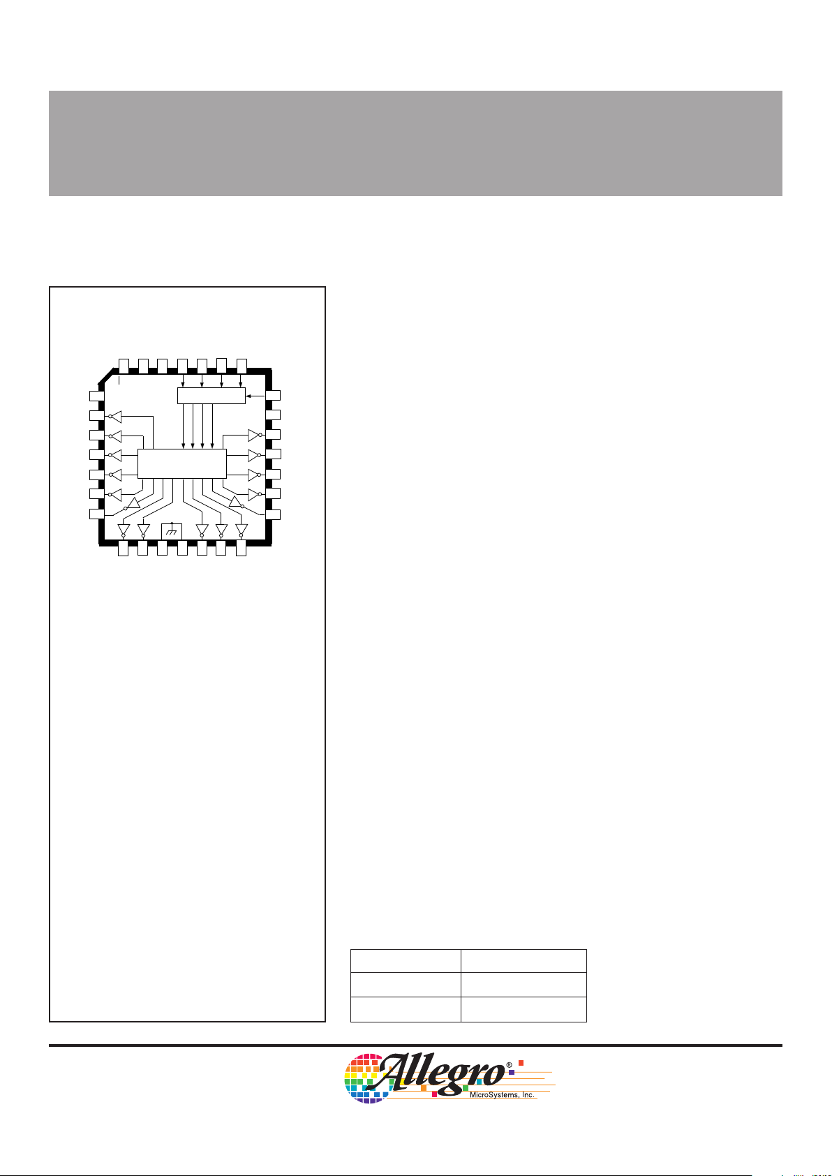
The UCN5816A and UCN5816EP 4-to-16 line latched decoder/
drivers combine low-power CMOS inputs and logic with 16 highcurrent, high-voltage bipolar outputs. The CMOS inputs cause minimal
loading and are compatible with standard CMOS, PMOS, and NMOS
logic. TTL or DTL circuits may require the use of appropriate pull-up
resistors to ensure an input logic high. The logic operates over a
supply range of 5 V to 12 V. A CHIP ENABLE function can be used
with two devices for 5-to-32 line decoding applications.
The 16 bipolar power outputs are open-collector 60 V Darlington
drivers capable of sinking 350 mA continuously. Internal transientsuppression diodes provide protection for use with inductive loads.
For ink-jet printer applications, the A5817SEP addressable 28-line
decoder/driver is recommended.
The UCN5816A is supplied in a 28-pin dual in-line plastic package
with 0.600" (15.24 mm) row spacing. The UCN5816EP is furnished in
a 28-lead plastic chip carrier (quad pack) for minimum-area surfacemount applications. Both devices will drive 350 mA loads continuously
over the full operating temperature range.
FEATURES
■ Addressable Data Entry
■ 60 V Minimum Output Breakdown
■ CMOS, PMOS, NMOS, TTL Compatible Inputs
■ Low-Power CMOS Logic and Latches
■ Output Transient Protection
■ Output Enable and Strobe Functions
5816
UCN5816EP
4-TO-16 LINE
LATCHED DECODER/DRIVERS
Always order by complete part number:
Part Number Package
UCN5816A 28-Pin DIP
UCN5816EP 28-Lead PLCC
ABSOLUTE MAXIMUM RATINGS
at T
A
= 25°C
Output Voltage, VCE . . . . . . . . . . . . . . 60 V
Logic Supply Voltage, V
DD
. . . . . . . . . 15 V
Input Voltage Range,
VIN . . . . . . . . . . . -0.3 V to VDD + 0.3 V
Output Current, I
C
. . . . . . . . . . . . . 500 mA
Package Power Dissipation,
PD . . . . . . . . . . . . . . . . . . . See Graph
Operating Temperature Range,
T
A
. . . . . . . . . . . . . . . -20°C to +85°C
Storage Temperature Range,
TS . . . . . . . . . . . . . . -55°C to +150°C
Caution: CMOS devices have input static
protection but are susceptible to damage when
exposed to extremely high static electrical
charges.
Data Sheet
26186.10
Page 2
5816
4-TO-16 LINE LATCHED DECODER/DRIVERS
115 Northeast Cutoff, Box 15036
Worcester, Massachusetts 01615-0036 (508) 853-5000
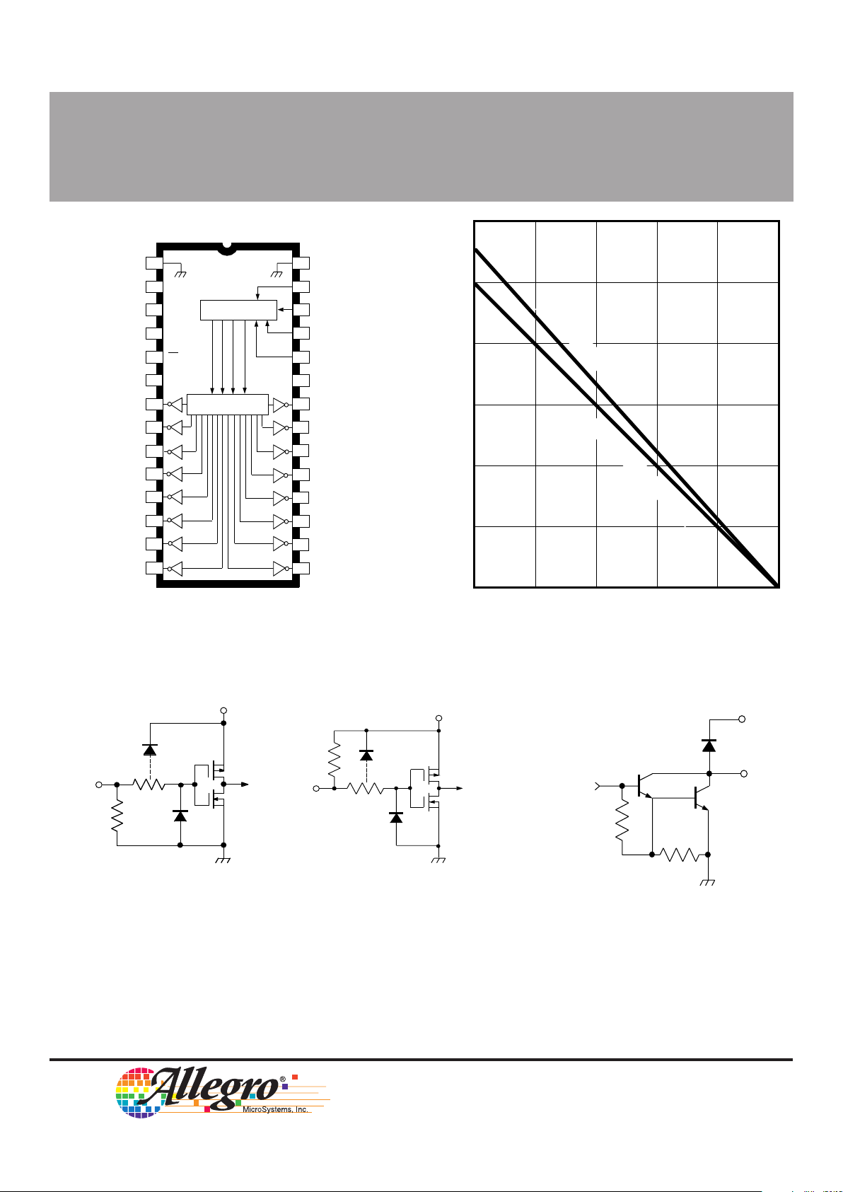
1
2
3
4
5
6
7
8
9
10
11
12
13
14 15
16
17
18
19
20
21
22
23
24
25
26
27
28
Dwg. PP-031
GROUND
CHIP
ENABLE
STROBE
V
OUTPUT
ENABLE
DIODE
COMMON
0-7
D
C
B
8-15
15
14
13
12
11
10
GROUND
IN
IN
IN
IN
OUT
OUT
OUT
OUT
OUT
OUT
OUT
OUT
DIODE
COMMON
A
9
8
OUT
0
OUT
1
OUT
3
OUT
2
OUT
4
OUT
5
OUT
6
OUT
7
DD
LOGIC
SUPPLY
LATCHES
DECODER
CE
ST
OE
K
K
50 75 100 125 150
2.5
0.5
0
ALLOWABLE PACKAGE POWER DISSIPATION IN WATTS
AMBIENT TEMPERATURE IN °C
2.0
1.5
1.0
25
3.0
Dwg. GP-028-1A
SUFFIX 'A', R = 45°C/W
θJA
SUFFIX 'EP', R = 55°C/W
θJA
UCN5816A
Dwg. EP-021-4
OUT
K
TYPICAL INPUT CIRCUITS TYPICAL OUTPUT DRIVER
Dwg. EP-010-3
IN
V
DD
Dwg. EP-010-4A
IN
V
DD
W
Copyright © 1984, 1995, Allegro MicroSystems, Inc.
Page 3

5816
4-TO-16 LINE LATCHED DECODER/DRIVERS
ELECTRICAL CHARACTERISTICS at T
A
= 25°C, V
DD
= 5 V (unless otherwise specified).
Leakage Current
Limits
Characteristic Symbol Test Conditions Min. Typ. Max. Units
Output Leakage Current I
CEX
VCE = 60 V, TA = +25°C——50µA
Output Saturation Voltage V
CE(SAT)
IC = 100 mA — 0.9 1.1 V
I
C
= 200 mA — 1.1 1.3 V
I
C
= 350 mA, VDD = 7.0 V — 1.3 1.6 V
Input Voltage V
IN(0)
-0.3 — 0.8 V
V
IN(1)
VDD = 12 V 10.5 — — V
V
DD
= 5.0 V 3.5 — 5.3 V
Input Resistance R
IN
VDD = 12 V 50 200 — kΩ
V
DD
= 5.0 V 100 600 — kΩ
Supply Current I
DD(ON)
VDD = 12 V, Outputs Open — 2.0 3.0 mA
VDD = 5.0 V, Outputs Open — 1.0 1.5 mA
I
DD(OFF)
All Drivers OFF, All Inputs = 0 V, — — 100 µA
OE = VDD = 5.0 V
All Drivers OFF, All Inputs = 0 V, — — 200 µA
OE = V
DD
= 12 V
Clamp Diode I
R
VR = 60 V, TA = +25°C——50µA
V
R
= 60 V, TA = +70°C — — 100 µA
Clamp Diode V
F
IF = 350 mA — 1.5 2.0 V
Forward Voltage
Page 4

5816
4-TO-16 LINE LATCHED DECODER/DRIVERS
115 Northeast Cutoff, Box 15036
Worcester, Massachusetts 01615-0036 (508) 853-5000
Information present at the inputs is
transferred to the latches when the STROBE
is high. The latches will continue to accept
new data as long as the STROBE is held
high. With the STROBE in the low state, no
information can be loaded into the latches.
Depending on the four address inputs, the
4-to-16 line decoder enables one of the
16 output sink drivers. When the OUTPUT
ENABLE is high, all of the outputs are
disabled (OFF) without affecting the information stored in the latches. When the OUTPUT ENABLE is low, the outputs are controlled by the information in the latches.
When the CHIP ENABLE is low, all of the
outputs are disabled (OFF). With two decoder/drivers and an inverter, the CHIP
ENABLE function can be used for 5-to-32 line
decoding applications.
QO = The output condition prior to the high-to-low transition of the STROBE input.
X = Irrelevant
CLEAR
STROBE
OUTPUT
ENABLE
IN
N
OUT
N
A
C
BC
B
G
D
E
F
A
C
B
G
E
p/o Dwg. No. A-10,895A
TIMING CONDITIONS
(Logic Levels are VDD and Ground)
A. Minimum Data Active Time Before Strobe Enabled
(Data Set-Up Time) . . . . . . . . . . . . . . . . . . . . . . . . . . . . . . . . . . 50 ns
B. Minimum Data Active Time After Strobe Disabled
(Data Hold Time) . . . . . . . . . . . . . . . . . . . . . . . . . . . . . . . . . . . . 50 ns
C. Minimum Strobe Pulse Duration . . . . . . . . . . . . . . . . . . . . . . . . . . . . 125 ns
D. Typical Time Between Strobe Activation and Output On to
Off Transition . . . . . . . . . . . . . . . . . . . . . . . . . . . . . . . . . . . . . . 500 ns
E. Typical Time Between Strobe Activation and Output Off to
On Transition . . . . . . . . . . . . . . . . . . . . . . . . . . . . . . . . . . . . . . 500 ns
G. Minimum Data Pulse Duration . . . . . . . . . . . . . . . . . . . . . . . . . . . . . 225 ns
TRUTH TABLE
CHIP IN
D
IN
C
IN
B
IN
A
OUTPUT OUTPUTS
STROBE ENABLE (MSB) (LSB) ENABLE (OFF unless otherwise specified)
1100000 OUT
0
ON
1100010 OUT
1
ON
1100100 OUT
2
ON
1100110 OUT
3
ON
1101000 OUT
4
ON
1101010 OUT
5
ON
1101100 OUT
6
ON
1101110 OUT
7
ON
1110000 OUT
8
ON
1110010 OUT
9
ON
1110100 OUT
10
ON
1110110 OUT
11
ON
1111000 OUT
12
ON
1111010 OUT
13
ON
1111100 OUT
14
ON
1111110 OUT
15
ON
0 1 X XXX 0 Q
O
X 0 X X X X X All OFF
X X X X X X 1 All OFF
 Loading...