

Page 1
All-Band AM/FM Receiver and Audio Amplifier
Description
The U2510B is an integrated bipolar one-chip AM/FM
radio circuit. It contains an FM front end with
preamplifier, FM IF and demodulator, a complete AM
Features
Superior FM strong signal behavior by using RF AGC
receiver, an AF amplifier and a mode switch for AM, FM
and tape. This circuit is designed for clock radios and
portable radio-cassette recorders.
DC mode control: AM, FM and tape
U2510B
Soft mute and HCC for decreasing interstation noise
in FM mode
Excellent AFC performance (level controlled, both
polarities available)
Level indicator (LED drive) for AM and FM
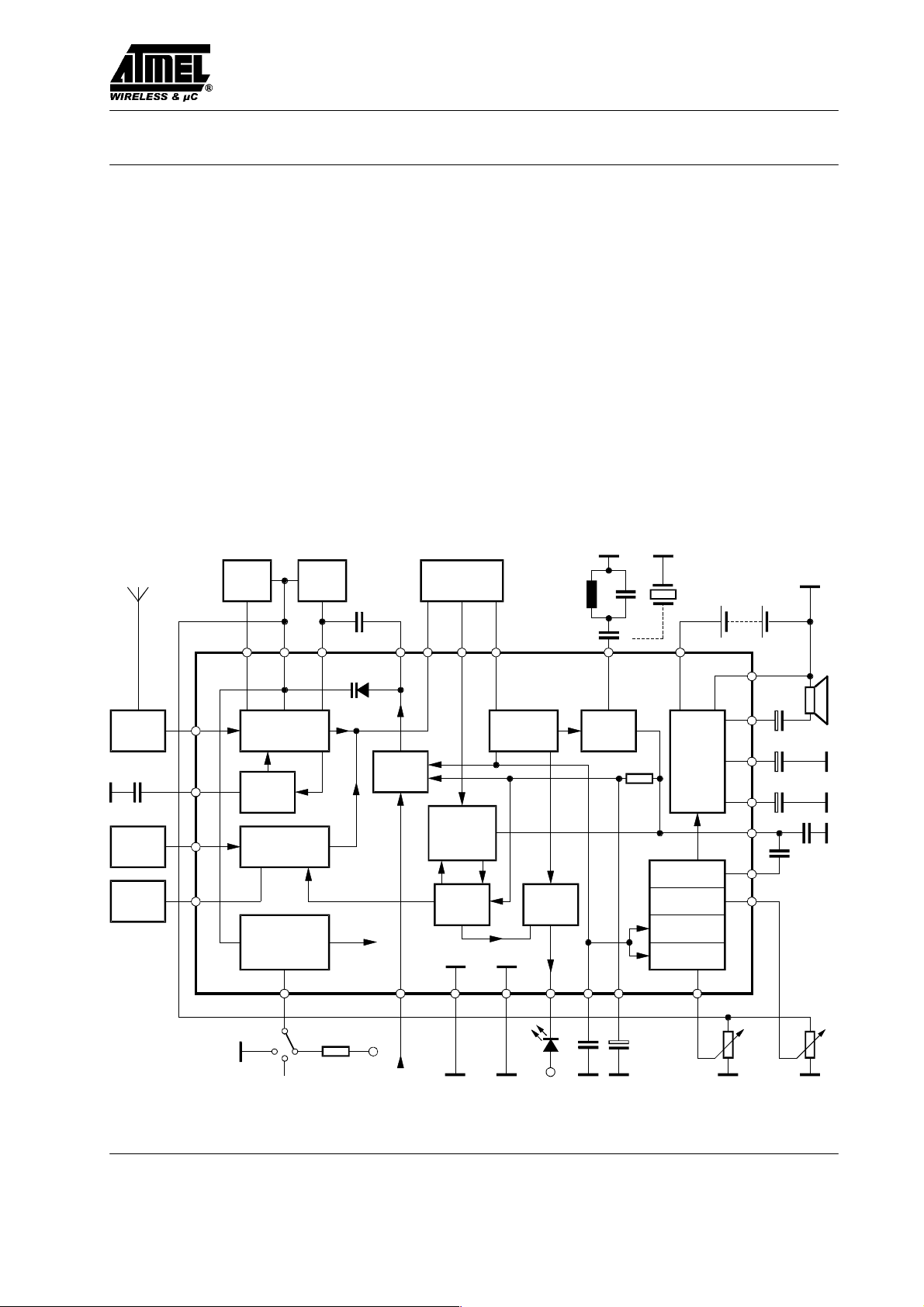
Block Diagram
FM osc.
tank
87 6
AFC
FM
front end
FM
AM
front end
RFAGC
AM/FM
and
15
IF BPE
14 16
AFC
control
AM IF
amp. and
detect.
IF
AGC
AGC
21 13 20 19 1
FM ant.
FM RF
BPE
AGC
AM
ant.
AM osc.
tank
12
11
10
5
V
Ref
FM RF
tank
9
AGC
Voltage stab.
mode control
Wide supply-voltage range and low quiescent current
High AF output power: 1 W
Electronic volume control
Electronic AF bandwidth control (treble and high cut)
Output stage for headphone and speaker drive
(Replaceable)
V
S
AM
IF
FM IF
amp.
Level
indic.
226
FM
discr.
22 18
Power
amp.
AF preamp.
Volume
Mute
HCC
28
27
3
25
23
24
4
S
AM
FM
2
Tape
V
S
AFC mode
Figure 1. Block diagram
LED
V
S
Treble Vol
13912
Rev. A3, 23-Feb-01 1 (15)
Page 2

U2510B
Order Information
Extended Type Number Package Remarks
U2510B-M SDIP28
U2510B-M__T SDIP28 VS < 6 V supply voltage
Pin Description
Mute
FM-discr
Vol ctrl in
AMOsc
FM-AFC
FMOsc
V
FMtank
AMtank
FM-AGC
FMin
FE-GND
AM/FM
IFout
CF
Ref
1
2
3
4
5
6
7
8
9
10
11
12
13
14
14812
Figure 2. Pinning
Pin Symbol Function
1 Mute Mute voltage output, time constant (C23),
2 FM-discr FM discriminator filter connection, ceramic
3 CF Audio negative feedback input. Blocking
4 Vol ctrl in Input for volume control voltage
mute depth and threshold adjustable by load
resistance (R3)
resonator or equivalent LC-circuit
capacitor (C8) determines the audio amplifiers
low-end cut-off frequency
28
27
26
25
24
23
22
21
20
19
18
17
16
15
AF-GND
AFout
V
S
Ripple in
AFin
AM/FM detect
V
AGC/AFC
AFC switch
IF-GND
LED drive
V
Treble in
FM-IFin
AM-IFin
Mode ctrl
switch
Pin Symbol Function
5 AMOsc AM oscillator tank circuit input, recommended
6 FM–AFC AFC diode connection, coupling capacitor
7 FMOsc FM oscillator tank circuit input, recommended
8 V
9 FMtank FM RF tank circuit connection, recommended
10 AMtank AM RF tank circuit connection, recommended
11 FM-AGC FM AGC voltage output, time constant (C20).
12 FMin FM RF input (common-base preamplifier
13 FE-GND FM front-end ground
14 AM/FM
15 Mode ctrl
16 AM-IFin AM IF input, input impedance = 3.1 k
17 FM-IFin FM IF input, input impedance = 330
18 V
19 LED drive Level indicator output
20 IF-GND IF ground
21 AFC switch AFC function control input:
22 V
23 AM/FM
24 AFin Audio amplifier input, input resistance
25 Ripple in Ripple filter connection. Load capacitance
26 V
27 AFout Audio amplifier output
28 AF-GND Ground of the audio power stage
IFout
switch
Treble in
AGC/AFC
detect
load impedance approximately 2.5 k
(C19) determines the AFC characteristic
(holding range and slope)
load impedance approximately 3 k
Regulated voltage output (2.4 V)
Ref
load impedance approximately 3 k
load impedance approximately 20 k
Loading this pin by a resistor (to GND) will
increase the FM AGC threshold, grounding
this pin will switch off the FM AGC function
transistor), recommended (RF) source
impedance approximately 100
AM/FM IF output
(collector output of the IF preamplifier)
Mode control input:
Pin | Function
open | F M
Ground | AM
VS (R4 = 10 k) | Tape
Treble control voltage input
(open-collector output, LED drive)
Pin | Function
open | AFC off
Ground | f
V
S
AGC/AFC voltage, time constant adjust (C10),
input impedance approximately 42 k
AM/FM detector output, the load capacitor
(C11) in conjunction with the detector output
resistance (7.5 k) determines the (FM)
deemphasis as well as the (modulation)
frequency response of the AM detector
approximately 100 k coupling capacitor
(C9) determines the low frequency response
(C12) determines the frequency response of the
supply-voltage ripple rejection
Supply voltage input
S
| f
OSC
OSC
> f
in
< f
in
Rev. A3, 23-Feb-012 (15)
Page 3

Terminal Voltages
Test circuit: Vin = 0
Pin Symbol
1 Mute voltage (R3 = 0) V
2 FM discriminator V
3 Negative feedback V
4 Volume control input (S4 = A) V
5 AM oscillator V
6 FM AFC V
7 FM oscillator V
8 V
Ref
9 FM RF tank V
10 AM input V
11 FM AGC V
12 FM input V
13 Front end ground V
14 AM/FM IF output V
15 Mode control switch V
16 AM IF input V
17 FM IF input V
18 Treble control input (S5 = A) V
19 LED V
20 IF ground V
21 AFC switch (S3 = off) V
22 AGC (AM)/AFC (FM) V
23 Detector output V
24 AF input V
25 Ripple filter V
26 Supply voltage V
27 AF output V
28 AF ground V
U2510B
Voltage/V
VS = 3 V VS = 6 V
AM FM TAPE AM FM TAPE
1
2
3
4
5
6
7
V
8
9
10
11
12
13
14
15
16
17
18
19
20
21
22
23
24
25
26
27
28
– 1.6 – – 1.6 –
– 1.0 – – 1.0 –
1.2 1.2 1.2 2.6 2.6 2.6
2.4 2.4 2.4 2.4 2.4 2.4
2.4 – – 2.4 – –
– 1.9 – – 1.9 –
– 2.4 – – 2.4 –
2.4 2.4 2.4 2.4 2.4 2.4
– 2.4 2.4 – 2.4 –
2.4 – – – 2.4 –
– 0 – – 0 –
1.4 – – 1.4 –
– – – – – –
2.9 2.7 – 5.9 5.7 –
0 – 2.9 0 – 5.7
0 – – 0 – –
– 0.7 – – 0.7 –
2.4 2.4 2.4 2.4 2.4 2.4
0 0 0 0 0 0
1.2 1.2 1.2 1.2 1.2 1.2
1.5 1.2 – 1.5 1.2 –
1.5 1.2 – 1.5 1.2 –
1.5 1.5 1.5 1.5 1.5 1.5
2.7 2.7 2.7 5.3 5.3 5.3
3.0 3.0 3.0 6.0 6.0 6.0
1.2 1.2 1.2 2.6 2.6 2.6
0 0 0 0 0 0
Rev. A3, 23-Feb-01 3 (15)
Page 4

U2510B
Absolute Maximum Ratings
Parameters Symbol Value Unit
Supply voltage V
Power dissipation P
Ambient temperature range T
Electrical Characteristics
S
tot
amb
13 V
900 mW
–20 to +75 °C
VS = 6 V, T
= 25°C, test circuit (figure 16), unless otherwise specified
amb
Parameters Test Conditions / Pins Symbol Min. Typ. Max. Unit
Supply voltage range V
Oscillator stop voltage V
S
S
2.5 9 * V
2.2 V
Operating temperature range T –20 +75 °C
Supply quiescent current Vi1 = Vi2 = V4 = 0;
AM (S2 = AM)
FM (S2 = FM)
TAPE (S2 = Tape)
Regulated voltage Pin 8 V
I
I
I
Ref
S
S
S
4.0
6.5
2.2
2.4 V
Audio amplifier Vi3 (Pin 24), test point: Vo (Pin 27) f = 1 kHz
AF measuring range: 30 Hz to 20 kHz, S2 = Tape, S4 = A, S5 = A
Input resistance Pin 24 R
Closed loop voltage gain GV
= 20 log (Vo/Vi3)
af1
Vi3 = 10 mV GV
Output voltage Vi3 = 100 mV, S4 = B V
High–end cut-off frequency fc (–3 dB)
S5 = B
Supply-voltage rejection ratio SVRR = 20 log (V
V
= 200 mV,
hum
f
= 200 Hz, S4 = B SVRR 32 dB
hum
hum/Vo
)
Noise voltage S4 = B, Vi3 = 0 V
j
af1
o
f
c
f
c
n
100 k
40 dB
0.7 3 mV
13
0.8
kHz
kHz
300 1000 V
AF output power THD = 10 %, RL = 8
VS = 4.5 V
VS = 6.0 V
VS = 9.0 V
P
o
P
o
P
o
400
225
420
1000
mW
mW
mW
Distortion Po = 50 mW, RL = 8 d 0.6 %
FM section, Vi2 = 60 dBV, fi2 = 98 MHz, fm = 1 kHz, dev. = 22.5 kHz, f
= 10.7 MHz,
iIF
AF measuring range: 300 Hz to 20 kHz, S2 = FM, S1 = A, S6 = B, test point: VD (Pin 23)
FM front-end voltage gain GVFM = 20 log (V
S1 = B, Vi2 = 40 dbV GV
Recovered audio voltage Pin 23 VD
Detector output resistance Pin 23 R
iIF
/ Vi2)
Do
FM
30 dB
af
85 mV
7.5 k
Detector output distortion dev. = 75 kHz
Vi2 = 60 dBV
Vi2 = 105 dBV
THD
THD
0.5
0.8
* U2510B-M__T: max. 6 V
mA
mA
mA
%
%
Rev. A3, 23-Feb-014 (15)
Page 5

Electrical Characteristics (continued)
U2510B
VS = 6 V, T
= 25°C, test circuit (figure 16), unless otherwise specified
amb
Parameters Test Conditions / Pins Symbol Min. Typ. Max. Unit
AM rejection ratio m = 30% AM
RF sensitivity (S+N)/N = 26 dB
(S+N)/N = 46 dB
Limiting threshold (-3 dB) V
RR
V
i2
V
i2
i2
Mute voltage Test point: Mute
Vi2 = 0
Vi2 = 60 dBV
V
V
mute
mute
Mute depth Referred to V0 at Vi2 = 0
S6 = A
S6 = C
AFC holding range f
> fin, S3 = A, S6 = A
OSC
V
10 dBV
i2
Vi2 = 20 dBV
Vi2 = 80 dBV
LED current I
Oscillator voltage eZ
= 2.5 k Pin 7 V
load
AM section Vi1 = 60 dBV, fi1 = 1.6 MHz, fm = 1 kHz, m = 30%, f
MD
MD
FHR
FHR
FHR
LED
OSC
= 455 kHz,
iIF
AF measuring range: 300 Hz to 20 kHz, (S2 = AM, S1 = B, test point: VD)
AM front end voltage gain GVAM = 20 log (V
iIF/Vi1
)
GV
AM
Vi1 = 20 dBV, S1 = A
Recovered audio voltage V
Detector output resistance Pin 23 R
Detector output distortion Vi1 = 60 dBV
Vi1 = 105 dBV
RF sensitivity (S+N)/N= 10 dB
(S+N)/N= 26 dB
(S+N)/N= 46 dB
AGC figure of merit referred
to V
D af
Vi1 = 105 dBV, voltage
drop (V
) = –10 dB FOM 100 dB
D af
IF input resistance Pin 16 Z
LED current I
Oscillator voltage Pin 5 V
D af1
Do
THD
THD
V
i1
V
i1
V
i1
i
LED
OSC
25 dB
9
22
3 dBV
1.8
0.4
26
20
no AFC
180
220
5.5 mA
180 mV
25 dB
70 mV
7.5 k
1
3
0
16
35
3.1 k
5.5 mA
160 mV
dBV
dBV
V
V
dB
dB
kHz
kHz
%
%
dBV
dBV
dBV
Rev. A3, 23-Feb-01 5 (15)
Page 6

U2510B
S
I ( mA )
9510396
U
V ( dB )
95 10397
10
T
=25°C
amb
8
6
AM
4
2
0
246810
VS ( V )
Figure 3. Quiescent current
50
without
40
30
with treble control
20
Vi=5mV
VS=6V
10
RL=8
T
=25°C
amb
0
0.01 0.1 1 10
f ( kHz )
treble control
Tape
FM
12
100
10000
1000
o
P ( mW )
100
RL=4
8
16
32
10
010
9510399
VS ( V )
Figure 6. AF section: Max. output power
40
32
o
P ( mW )
24
16
246810
95 10400
VS ( V )
f=1kHz
d=10%
T
amb
V
hum
VS=6V
RL=8
T
=25°C
amb
=25°C
50
f=200Hz
f=100Hz
=200mV
12
d ( % )
95 10398
Figure 4. AF section
10
f=1kHz
T
=25°C
amb
8
6
VS=3V
RL=32
VS=6V
RL=8
4
2
0
1 10 100 1000
Po ( mW )
Figure 5. AF section: Distortion
VS=9V
RL=8
10000
Figure 7. AF section: Supply-voltage rejection ratio
o
V ( dBV )
95 10403
2.0
1.6
R3=∞
1.2
100k
0.8
68k
0.4
0
–20 0 20 40 60
Vi ( dBV )
VS=6V
T
=25°C
amb
80 100
Figure 8. FM section: Mute voltage
Rev. A3, 23-Feb-016 (15)
120
Page 7

U2510B
0
S+N(m=80%)
–20
S+N(m=30%)
–40
D
V ( dBV )
–60
N
VS=6V
fi1=1.6MHz
fAF=1kHz
T
=25°C
amb
–80
d(m=80%)
–100
d(m=30%)
–20 0 20 40 60
95 10404
Vi ( dBV )
Figure 9. AM section: Demodulator output level
0
VS=6V
Vi3=10mV
–20
–40
O
V ( dBV )
–60
fAF=1MHz
fAF=10kHz
T
=25°C
amb
Treble Voltage V
8
Treble Voltage = 0
6
5
4
AM
FM
I
LED
3
LED
I ( mA )
2
1
VS=6V
T
=25°C
amb
0
120
10080
95 10407
020406080
Vi ( dBV )
100
120
Figure 11. AM/FM level indicator current
2.0
1.2
0.8
AGC
V ( V )
VS=6V
0.4
fi1=1.6MHz
T
=25°C
amb
–80
0 0.5 1 1.5 2
95 10406
V4 ( V )
Figure 10. Volume control range characteristics
2.5
0
95 10408
20 0 20 40 60
Vi ( dBV )
80 100
Figure 12. AM section: AGC voltage (at Pin 22)
120
Rev. A3, 23-Feb-01 7 (15)
Page 8

U2510B
D
V ( dBV )
95 10401
68k
100k
95 10402
0
–20
–40
–60
–80
–100
–20 0 20
Figure 13. FM section: Demodulator output level
0
R3=0
–20
∞
–40
o
V ( dBV )
–60
–80
–100
–20 0 20 40 60
S+N(f=75kHz)
S+N(f=22.5kHz)
AM(m=30%)
N
40 60
80
Vi ( dBV )
AM
Vi ( dBV )
N
d
80 100
S+N
120100
120
V
= 6 V
S
f
= 98 MHz
i2
f
= 1 kHz
AF
T
= 25°C
amb
d(f=75kHz)
d(f=22.5kHz)
V
= 6 V
S
R
= 8
L
P
= 50 mW at
o
V
= 60 dBV
i2
f
= 98 MHz
i2
f
= 1 kHz
AF
f = 22.5 kHz
m
= 30%
AM
T
= 25°C
amb
O
V ( dBV )
–100
95 10405
Figure 14. FM section: Audio output level
0
S+N
–20
–40
d
–60
–80
–20 0 20 40 60
80 100
Vi ( dBV )
Figure 15. AM section: Audio output level
N
P
= 50 mW at
o
V
= 60 dBV
i1
R
= 8
L
f
= 98 MHz
i1
f
= 1 kHz
AF
m = 80%
T
= 25°C
amb
120
Rev. A3, 23-Feb-018 (15)
Page 9

Test Circuit
V
i1
(50 Ω)
V
i2
50 Ω
AM IFT
T
R
8
455 kHz
1
CF
(50 Ω)
R
100 Ω
R
75 Ω
1
U2510B
R
5
150Ω
C
24
6
100 nF
C
25
7
10 nF
14
L
A
150 µH
13 12 11 10 9 8 7
43 pF
C
22 nF
C
C
3
2
22 pF
20
C7C
4.7 µF
L
1
L
2
22 nF
C
18 pF
2.2 kΩ
6
U2510B
T
4
2
R
4
C
19
5.6 pF
654321
C
22 pF
C
8
4.7 µF
5
C
100
B
A
S
4
T
4
25
pF
C
18 pF
B
A
S
5
R
3
Ω
150 k
C
23
68 nF
C
B
S
24
6
V
A
mute
15 16 17
CF
Tape
2
FM
AM
2
10.7 MHz
R
1
390 Ω
R
2
10 kΩ
S
BA BA
1
V
iIF
R
3 kΩ
S
9
C
21
10 nF
19 20
18
C
22
10 nF
LEDD
1
100 nF
I
LED
Figure 16. Test circuit
Application
General
The U2510B is a bipolar monolithic IC for use in radio
sets, for example, headphone receivers, radio recorders
and clock radios. The IC contains all AM, FM, AF and
switching function blocks necessary to construct these
kinds of radio receivers using only few components
around the IC. In the design, special efforts were made to
get good performance for all AM bands (short and long
wave).
The implementation of enhanced functions (options)
makes it possible to improve the radio’s performance and
to produce radios with interesting features. In this case
few (external) parts have to be changed or added. By
using all or some of the options offered by the U2510B
different types or classes of radios can be designed to the
customer ’s requirements with the same IC.
A
off
C14C
21
S
3
B
10 µF
23
22
C
9
10 nF
C
10
11
10 nF
V
D
24
C
10 µF
V
i3
25 26
12
470 µF
27
28
C
15
220µF
C
13
R
L
8Ω/
2 W
V
V
S
GND
o
One of the general advantages of using the U2510B is the
fact that all receiver functions (including the options) are
integrated and tested on a system level. Therefore, two
additional cost-savings are achieved by:
1. Shorter development time through less technical
problems and
2. Higher reproductivity and low reject level in the set
production line.
Another advantage, due to the technology of the
U2510B, is the wide operating voltage range, especially the upper limit (13 V). This feature allows the
use of soft power supply for line powered radios
which can also reduce the set’s total cost.
13913
Rev. A3, 23-Feb-01 9 (15)
Page 10

U2510B
Circuit Example
Figure 17 shows a circuit diagram for low end AM/AF
radios using the U2510B. Figure 18 shows a circuit
diagram of AM/AF radio for higher class designs using all
possible options of the U2510B. The layout of the PC
board, shown in figure 19, is suitable for both the circuit
example shown in figure 17 and the circuit example
shown in figure 18. The associated coil, varicon and filter
specifications are listed in the table: COIL DATA and
SPECIAL COMPONENT PARTS. The circuit diagram
(figure 18), has the following options compared to the
circuit diagram (figure 17) (the additional parts, which
have to be provided, are listed in parentheses):
a) Soft mute and high cut control in FM mode (1 cap.)
b) Electronic treble control in AM, FM and TAPE mode
(1 pot.)
c) On-chip mode control for TAPE application
d) RF AGC in FM mode (1 capacitor)
e) AFC, adjustable to the correct polarity and slope
(1 cap.)
f) Tuning indication using LED as an indicator
(1 LED, 1 cap.)
Option a) reduces the interstation noise by the two
functions: soft mute and HCC. Both are controlled by the
mute voltage (Pin 1). The soft mute reduces the loudness
only, while the HCC reduces the high-end audio cut-off
frequency of the audio preamplifier, when the signal level
falls below a given threshold. This signal level threshold
as well as the mute depth can be reduced by adding a
resistor (R3) or by increasing the FM front–end gain.
Option b) allows the treble control for all operating modes
without the need of an additional capacitor. This concept
leads to a smooth and correct treble control behavior
which is an improvement compared to the controlled RC
network normally used.
Option c) is very useful for application in radio
cassette-recorders, for instance. In TAPE mode, the
AM/FM receiver blocks are completely switched off and
the signal from the tape recorder can be fed to the audio
amplifier ’s input directly. This saves quiescent current
and makes the TAPE switching easy. However, to
minimize switching noise by the mode switch, the
following switch sequence should be chosen: AM, FM,
TAPE.
Option e) improves the tuning behavior substantially. The
special design of the on-chip AFC function means that
common disadvantages such as asymmetrical slope,
(chip-) temperature effects and unlimited holding range
are avoided. As mentioned in the “Pinning Description
Table”, the AFC slope has to be inverted when the local
oscillator (LO) frequency has to be below the receiving
frequency. This can be achieved by connecting Pin 21 to
the potential of Pin 8. In addition to the options described
above, the following proposals are implemented in the
circuit diagram (figure 18), too:
An FM IFT is applied. This improves the channel
selectivity and minimizes substantially the spurious
responses caused by the FM ceramic filter (CF2). With
the choice of the winding ratio of this IFT, the FM
front end gain can be matched to other values if necessary.
In the FM RF input section, the low cost antenna filter
(L5, C15) is replaced by a special band pass filter
(PFWE8). Such a BPF protects the FM front end
against the out-off-band interference signals (TV
channels, etc.) which could disturb the FM reception.
Design Hints
The value of the power supply blocking capacitor C
should not be below 470 F. In addition, this capacitor
should be placed near Pin 26. This will help to avoid
unacceptable noise generated by noise-radiation from the
audio amplifier via the bar-antenna. In designs, where the
supply voltage goes below 2.5 V, the value of the blocking
capacitor (C7) should be chosen as 47 F or even higher.
To achieve a high rejection of short wave reception in
medium wave operation, the LO amplitude at Pin 5
should not exceed approximately 200 mV. This LO
amplitude depends on the LO transformer’s Q and its
turns ratio. For the LO transformer type described in the
“Coil Data Table”, a resistor R4 (2.2 k for example) in
parallel to the secondary side of the AM LO transformer
T2 is recommended. To minimize feedback effects in the
RF/IF part in FM mode, the capacitor C6 should be placed
as near to Pins 8 and 20 as possible.
As shown in the application circuit diagrams (figures 17
and 18), in FM mode ceramic filter devices are used for
channel selection (CF2) while for FM, demodulation in
LC-discriminator circuit (T4, C24, C25) is used instead of
a ceramic discriminator device.
13
Option d) improves the strong signal behavior by
protecting the FM mixer against overload. This is
provided by the integrated broad-band-width RF AGC. If
necessary, the AGC threshold can be decreased by a
resistor, loading Pin 11 to GND (not shown).
Such an LC discriminator circuit can be easily matched
to the FM IF selectivity block by its alignment. The zerocrossing of the discriminator can be detected at the
demodulator output (Pin 23). The zero-crossing voltage
is equal to half of the regulated voltage at Pin 8.
Rev. A3, 23-Feb-0110 (15)
Page 11

U2510B
The alignment of the LC-discriminator circuit should be
done with little or no effect on the AFC function. This can
be realized by:
– switching Pin 21 to open-circuit
– connecting Pin 1 to a voltage source of 2 V
– using a low signal level for alignment.
Application Circuits
Antenna
AMFM
C
2
3
22 pF
AM IFT
T
L
C
3
C
16
33 pF
C
C
33 pF
455 kHz
1
CF
1
17
18
33 pF
L
4
13 12 11 10 9 8 7
14
2 pF
In general, ceramic discriminator devices can be used,
too. In this case, the effect of unavoidable spreads in the
frequency characteristics of these case ceramic devices in
conjunction with the IC characteristic has to be considered. For example, mismatches of the characteristics
between selectivity block and FM discriminator will lead
to an increased signal-to-noise ratio at low signal level as
well as to a higher demodulation distortion level or to an
asymmetrical AFC.
T
2
4
4.7 µF
654321
C
5
Volume
6 pF
T
4
C
25 100 pF
C
8
C
18 pF
24
P
50 kΩ
C7C
4.7 µF
C
27 pF
L
L
2
1
6
22 nF
U2510B
1
R
1
390 Ω
S
2
15 16 17
CF
2
AM
FM
10.7 MHz
19 20
18
21
C
4.7 µF
23
22
C
9
10 nF
C
10
11
10 nF
24
C
4.7 µF
25 26
12
470 µF
27
28
C
15
220 µF
100 nF
C
14
Z = 8 Ω
C
13
S
1
V
S
13915
Figure 17. Application circuit (low cost)
Rev. A3, 23-Feb-01 11 (15)
Page 12

U2510B
Antenna
AMFM
L
3
2 pF
C
C
2
3
22 pF
27 pF
L
L
2
1
T
C
2
4
6 pF
C
Volume
5
P
1
50 kΩ
Treble
P
2
50 kΩ
100 pF
AM IFT
T
AM IFT
T
BPF 1
C
7C6
22 nF
4.7 µF
C
20
22 pF
14
13 12 11 10 9 8 7
455 kHz
1
CF
1
R
4
2.2 kΩ
C
5.6 pF
19
C
8
4.7 µF
18 pF
654321
T
4
C
100 pF
25
C
23
68 nF
)
(R
C
3
24
Mute
Adj.
U2510B
3
CF
2
10.7 MHz
R
15 16 17
S
Tape
FM
AM
2
C
21
10 k
10 nF
19 20
18
C
22
21
10 nF
LEDD
1
2
Ω
C
10 µF
23
22
C
9
22 nF
C
10
11
10 nF
IN Tape
24
C
4.7 µF
25 26
12
470 µF
27
28
C
15
220 µF
100 nF
C
14
C
13
S
1
V
S
13914
Figure 18. Application circuit (upgraded) R2 only if V
Figure 19. PC-board
> 8 V
S
Rev. A3, 23-Feb-0112 (15)
Page 13

Coil Data and Special Component Part
U2510B
Part Stage L or C
between
T1AM IFT 180 pF
1 to 3
T2AM OSC 270 H
1 to 3
T3FM IFT
(optional)
T4FM discrimi-
nator
100 pF
1 to 3
100 pF
1 to 3
L1FM RF
air coil
4 mm diam.
L2FM OSC
air coil
4 mm diam.
L4FM antenna
air coil
4 mm diam.
Q0 between Wire diameter/mm
0
Terminal No.
Number of turns
90
1 to 3
0.07
1 to 2
111
125
1 to 3
0.06
1 to 3
107
0.09
1 to 2
3
0.09
1 to 3
10
0.62
3.75
0.62
3.75
0.62
4.75
0.07
2 to 3
35
0.06
4 to 6
29
0.09
2 to 3
7
0.07
4 to 6
7
0.09
4 to 6
2
Type
Manufacturer
7MC-7789N
Toko
21K7-H5
Mitsumi
7TRS-8441
Toko
L-5K7-H5
Mitsumi
mat.:
7P A119 AC
Toko
mat.:
7P A119 AC
Toko
L
3
AM bar antenna L: 630 H total turns : 96 tap: 19
BPF1 (optional) PFWE8 (88 to 108 MHz) Soshin Electric Co.
CF
1
CF
2
CF
C
3
1
3
2
4
(optional) CDA10.7MC1 Murata
Variable capacitor HD22124 AM/FM Toko
4 mm
4
6
Coil, bottom view Air coil AM bar antenna
SFU-455B
BFCFL-455
SFE10.7MA5
CFSK 107M1
Figure 20.
Murata
Toko
Murata
Toko
3 mm 80 mm
18 mm
1
Pin 10C
Pin 8
13931
Rev. A3, 23-Feb-01 13 (15)
Page 14

U2510B
Package Information
Package SDIP28
Dimensions in mm
27.5
27.1
4.8
4.2
10.26
10.06
0.9
3.3
0.53
23.114
1
0.43
1.778
technical drawings
according to DIN
specifications
0.35
0.25
8.7
8.5
12.2
11.0
13044
Rev. A3, 23-Feb-0114 (15)
Page 15

U2510B
Ozone Depleting Substances Policy Statement
It is the policy of Atmel Germany GmbH to
1. Meet all present and future national and international statutory requirements.
2. Regularly and continuously improve the performance of our products, processes, distribution and operating systems
with respect to their impact on the health and safety of our employees and the public, as well as their impact on
the environment.
It is particular concern to control or eliminate releases of those substances into the atmosphere which are known as
ozone depleting substances (ODSs).
The Montreal Protocol (1987) and its London Amendments (1990) intend to severely restrict the use of ODSs and forbid
their use within the next ten years. Various national and international initiatives are pressing for an earlier ban on these
substances.
Atmel Germany GmbH has been able to use its policy of continuous improvements to eliminate the use of ODSs listed
in the following documents.
1. Annex A, B and list of transitional substances of the Montreal Protocol and the London Amendments respectively
2. Class I and II ozone depleting substances in the Clean Air Act Amendments of 1990 by the Environmental
Protection Agency (EPA) in the USA
3. Council Decision 88/540/EEC and 91/690/EEC Annex A, B and C (transitional substances) respectively.
Atmel Germany GmbH can certify that our semiconductors are not manufactured with ozone depleting substances
and do not contain such substances.
We reserve the right to make changes to improve technical design and may do so without further notice.
Parameters can vary in different applications. All operating parameters must be validated for each customer
application by the customer. Should the buyer use Atmel Wireless & Microcontrollers products for any unintended
or unauthorized application, the buyer shall indemnify Atmel Wireless & Microcontrollers against all claims,
costs, damages, and expenses, arising out of, directly or indirectly, any claim of personal damage, injury or death
associated with such unintended or unauthorized use.
Data sheets can also be retrieved from the Internet: http://www.atmel–wm.com
Atmel Germany GmbH, P.O.B. 3535, D-74025 Heilbronn, Germany
Telephone: 49 (0)7131 67 2594, Fax number: 49 (0)7131 67 2423
Rev. A3, 23-Feb-01 15 (15)
 Loading...