

Page 1
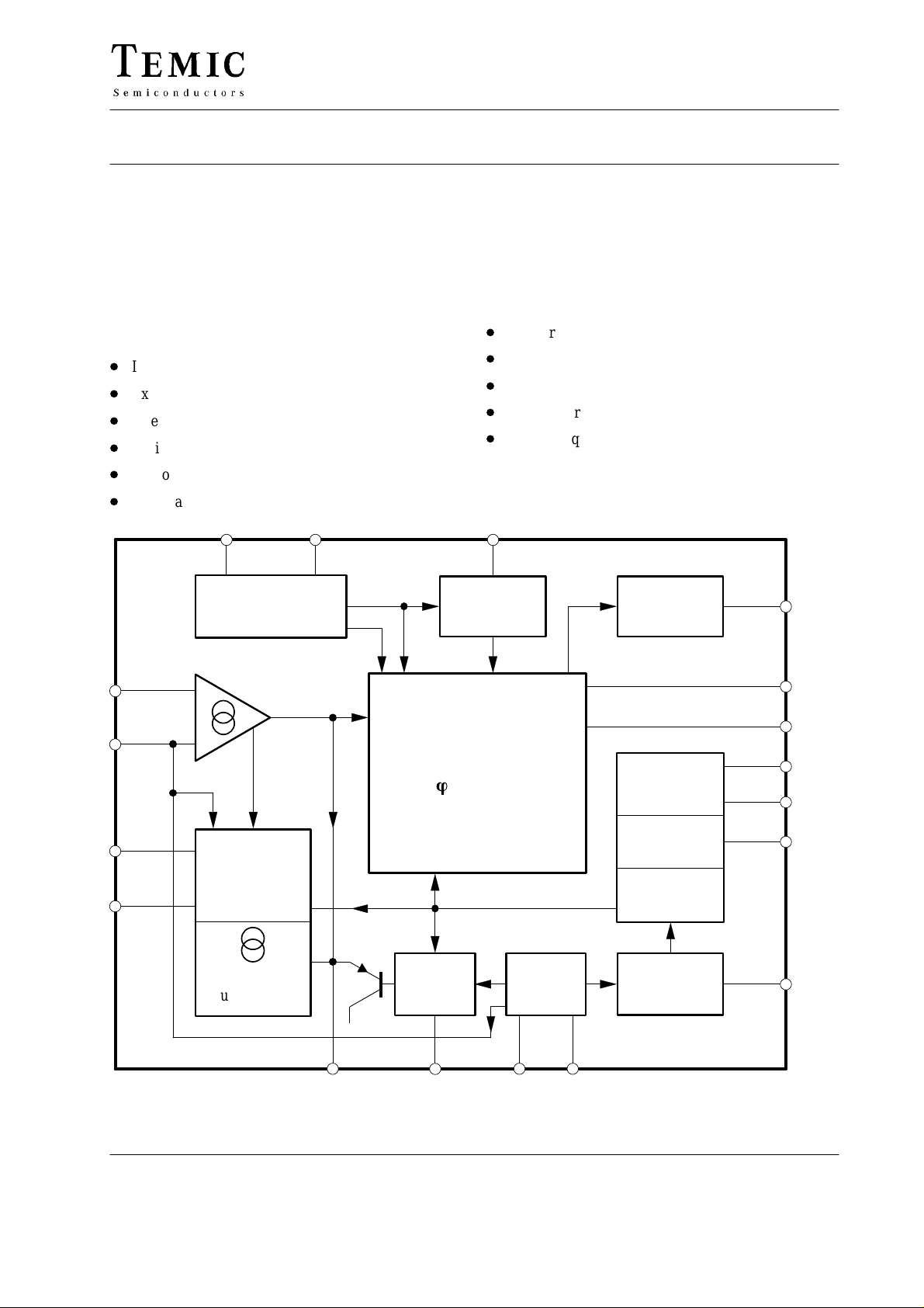
U211B2/ B3
Phase Control Circuit - General Purpose Feedback
Description
The integrated circuit U211B2/ B3 is designed as a phase
control circuit in bipolar technology with an internal frequency-voltage converter. Furthermore, it has an internal
control amplifier which means it can be used for speedregulated motor applications.
Features
D
Internal frequency-to-voltage converter
D
Externally-controlled integrated amplifier
D
Overload limitation with a “fold back” characteristic
D
Optimized soft-start function
D
Tacho monitoring for shorted and open loop
D
Automatic retriggering switchable
It has an integrated load limitation, tacho monitoring and
soft-start functions, etc. to realize sophisticated motor
control systems.
D
Triggering pulse typ. 155 mA
D
Voltage and current synchronization
D
Internal supply-voltage monitoring
D
Temperature reference source
D
Current requirement ≤ 3 mA
Package: DIP18 - U211B2,
SO16 - U211B3
11(10)
10(9)
14(13)
15(14)
17(16) 1(1)
Voltage / Current
detector
Control
amplifier
+
–
Load limitation
speed / time
controlled
controlled
current sink
5*)
Automatic
retriggering
Phase
control unit
ö
= f (V12)
Soft start
–V
Ref
12(11) 13(12) 9(8) 8(7)
Frequency-
to-voltage
converter
Output
pulse
Supply
voltage
limitation
Reference
voltage
Voltage
monitoring
Pulse-blocking
tacho
monitoring
4(4)
6(5)
7(6)
3(3)
2(2)
16(15)
18*)
95 10360
–V
S
GND
TELEFUNKEN Semiconductors
Rev . A1, 29-May-96
Figure 1. Block diagram (Pins in brackets refer to SO16)
*) Pins 5 and 18 connected internally
1 (20)
Page 2
U211B2/ B3
L
M
1
D
W
18 k
1N4007
1
R
2 W
R
R
4
3
W
470 k
W
220 k
=
M
V
TIC
226
12
R
4
5
17 1
Set speed
voltage
230 V ~
8
R
W
W
1 M
180
2
R
6
pulse
Output
Automatic
retriggering
detector
Control
amplifier
Voltage / Current
11
W
19
R
100 k
10
C
W
1 W
33 m
3.3 nF
C
7
–
+
10
F
m
2.2 /16V
N
F
m
22
C
S
2
–V
3
Supply
voltage
Phase
control unit
F
m
25 V
2.2
1
C
GND
2
limitation
)
12
= f (V
ö
10
R
11
16
voltage
Voltage
Reference
controlled
speed / time
Load limitation
14
W
W
1 k
1 M
monitoring
15
9
R
C
tacho
Pulse blocking
to voltage
Frequency
Soft start
controlled
current sink
F
m
9
4.7 /16V
18
monitoring
converter
Ref
–V
12 13 9 8
95 10361
220 nF
11
R
Speed sensor
4
C
W
R
1 k
5
F
1 nF
C
m
16 V
2.2
3
8
C
C
220 nF
7
R
7
F
m
10 /16V
W
2 M
6
R
6
C
W
22 k
W
100 k
100 nF
C
voltage
Actual speed
5
2 (20)
R
31
W
100 k
W
13
R
47 k
W
14
R
56 k
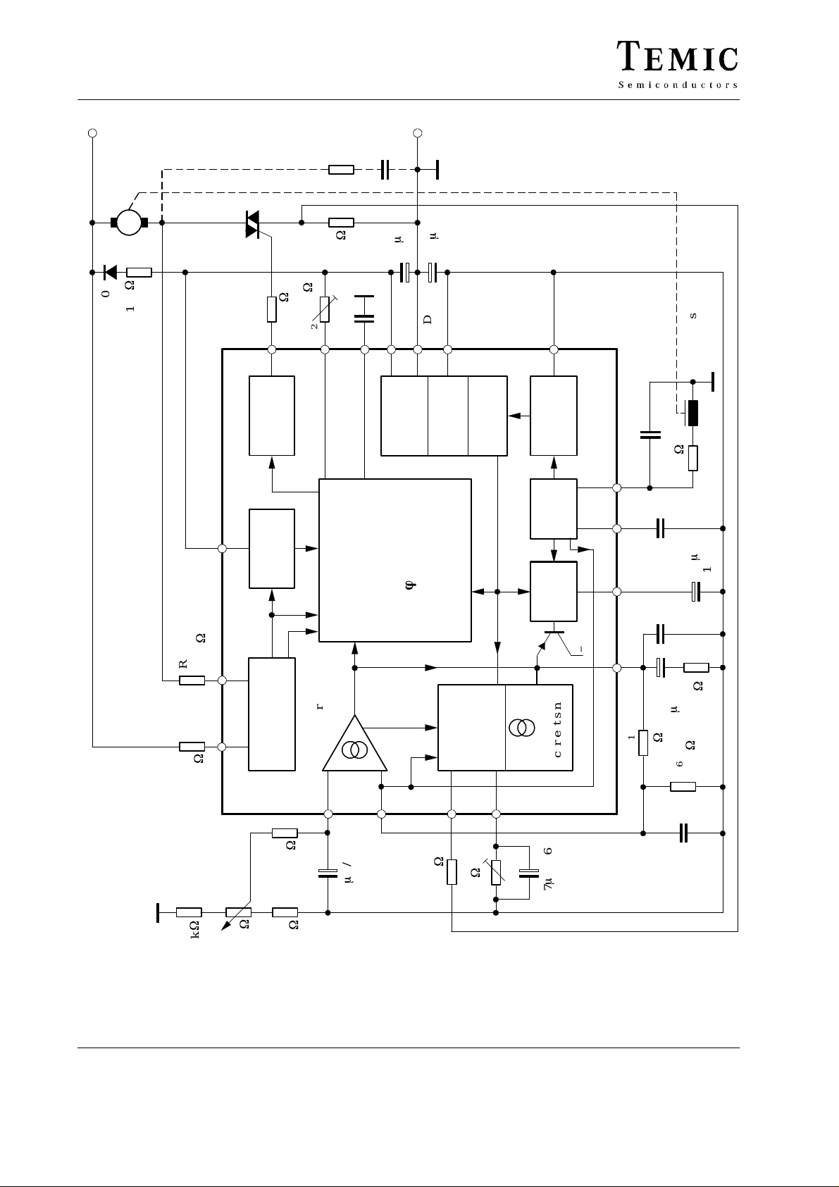
Figure 2. Speed control, automatic retriggering, load limiting, soft start
TELEFUNKEN Semiconductors
Rev . A1, 29-May-96
Page 3
Description
Mains Supply
The U211B2 is fitted with voltage limiting and can
therefore be supplied directly from the mains. The supply
voltage between Pin 2 (+ pol/ă) and Pin 3 builds up
and R
across D
1
series resistance can be approximated using (see
figure 2):
Further information regarding the design of the mains
supply can be found in the data sheets in the appendix.
The reference voltage source on Pin 16 of typ. –8.9 V is
derived from the supply voltage and is used for
regulation.
Operation using an externally stabilised DC voltage is not
recommended.
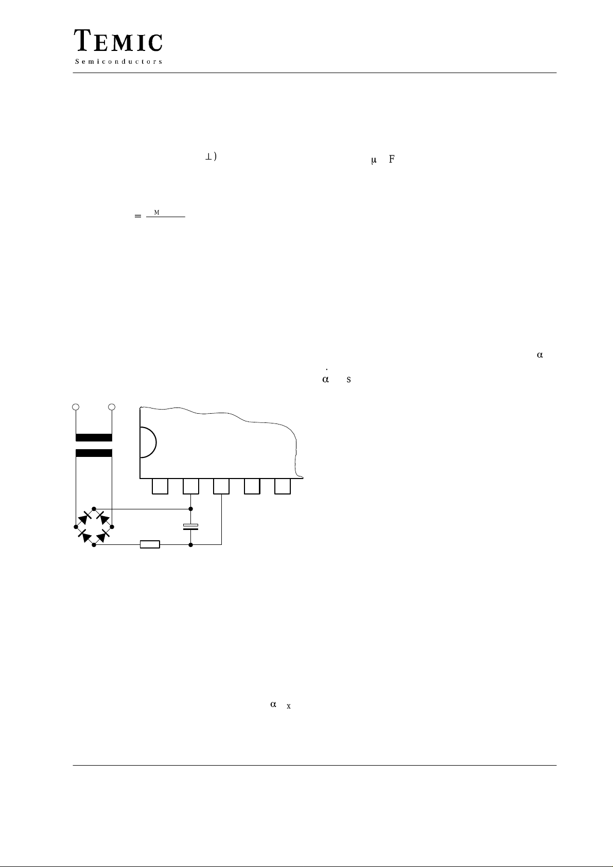
If the supply cannot be taken directly from the mains
because the power dissipation in R
then the circuit shown in the following figure 3 should be
used.
and is smoothed by C1. The value of the
1
V
–V
M
2I
S
S
would be too large,
1
+
R
1
U211B2/ B3
When the potential on Pin 7 reaches the nominal value
predetermined at Pin 12, then a trigger pulse is generated
whose width t
and hence the pulse width can be evaluated by
of C
2
is determined by the value of C
p
assuming 8 ms/nF). At the same time, a latch is set, so that
as long as the automatic retriggering has not been
activated, then no more pulses can be generated in that
half cycle.
The current sensor on Pin 1 ensures that, for operations
with inductive loads, no pulse will be generated in a new
half-cycle as long as a current from the previous half
cycle is still flowing in the opposite direction to the
supply voltage at that instant. This makes sure that “gaps”
in the load current are prevented.
The control signal on Pin 12 can be in the range 0 V to
–7 V (reference point Pin 2).
= –7 V then the phase angle is at maximum =
If V
12
i.e., the current flow angle is a minimum. The phase angle
a
is minimum when V
min
= V2.
12
(the value
2
a
max
~
24 V~
123
C
R
1
Figure 3. Supply voltage for high current requirements
1
4
95 10362
5
Phase Control
There is a general explanation in the data sheet,
TEA1007, on the common phase control function. The
phase angle of the trigger pulse is derived by comparing
the ramp voltage (which is mains synchronized by the
voltage detector) with the set value on the control input
Pin 12. The slope of the ramp is determined by C
charging current. The charging current can be varied
using R
also be adjusted using R
on Pin 6. The maximum phase angle
2
.
2
2
a
max
and its
can
Voltage Monitoring
As the voltage is built up, uncontrolled output pulses are
avoided by internal voltage surveillance. At the same
time, all of the latches in the circuit (phase control, load
limit regulation, soft start) are reset and the soft-start
capacitor is short circuited. Used with a switching
hysteresis of 300 mV, this system guarantees defined
start-up behavior each time the supply voltage is switched
on or after short interruptions of the mains supply.
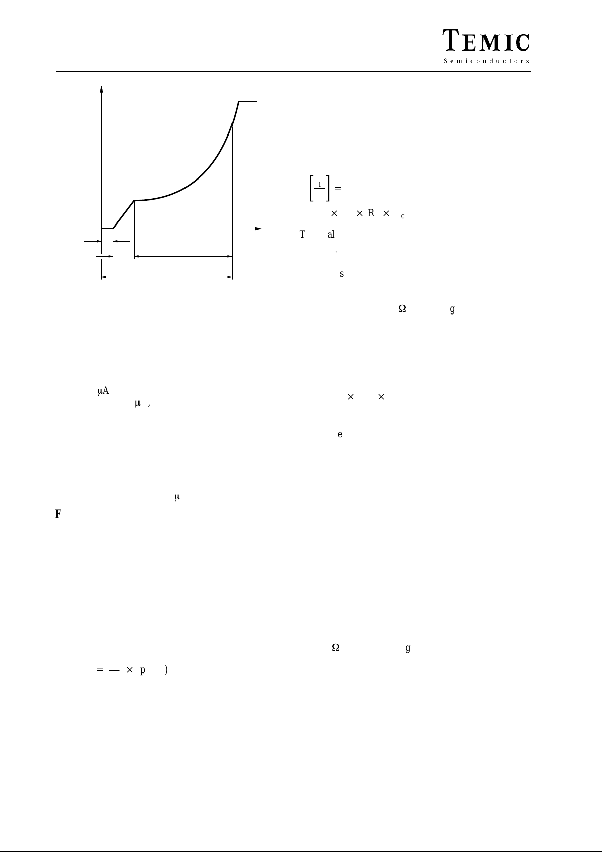
Soft-Start
As soon as the supply voltage builds up (t1), the integrated
soft-start is initiated. The figure below shows the
behaviour of the voltage across the soft-start capacitor
and is identical with the voltage on the phase control input
on Pin 12. This behaviour guarantees a gentle start-up for
the motor and automatically ensures the optimum run-up
time.
TELEFUNKEN Semiconductors
Rev . A1, 29-May-96
3 (20)
Page 4
U211B2/ B3
V
C3
V
12
V
0
t
1
t
2
Figure 4. Soft-start
t
3
t
tot
95 10272
t
t1 = build-up of supply voltage
= charging of C3 to starting voltage
t
2
+ t2 = dead time
t
1
= run-up time
t
3
= total start-up time to required speed
t
tot
C
is first charged up to the starting voltage V
3
typical 45 mA current (t
). By then reducing the charging
2
0
with
current to approx. 4 mA, the slope of the charging function
is substantially reduced so that the rotational speed of the
motor only slowly increases. The charging current then
increases as the voltage across C
increases giving a
3
progressively rising charging function which accelerates
the motor more and more strongly with increasing
rotational speed. The charging function determines the
acceleration up to the set-point. The charging current can
have a maximum value of 55 mA.
Frequency to Voltage Converter
The internal frequency to voltage converter (f/Vconverter) generates a DC signal on Pin 10 which is
proportional to the rotational speed using an AC signal
from a tacho-generator or a light beam whose frequency
is in turn dependent on the rotational speed. The high
impedance input Pin 8, compares the tacho-voltage to a
switch-on threshold of typ. –100 mV. The switch-off
threshold is given with –50 mV. The hysteresis
guarantees very reliable operation even when relatively
simple tacho-generators are used. The tacho-frequency is
given by:
n
f
+
60
where: n = revolutions per minute
p(Hz)
p = number of pulses per revolution
The converter is based on the charge pumping principle.
With each negative half wave of the input signal, a
quantity of charge determined by C
amplified and then integrated by C
is internally
5
at the converter
6
output on Pin 10. The conversion constant is determined
, its charge transfer voltage of Vch, R6 (Pin 10) and
by C
5
the internally adjusted charge transfer gain.
I
10
ƪ
ƫ
G
k = G
+
i
8.3
I
9
C5 R6 V
i
ch
The analog output voltage is given by
V
= k @ f
O
The values of C
and C
5
must be such that for the highest
6
possible input frequency, the maximum output voltage
does not exceed 6 V. While C5 is charging up, the R
V
O
on Pin 9 is .approx. 6.7 kW. To obtain good linearity of the
f/V converter the time constant resulting from R
and C
i
should be considerably less (1/5) than the time span of the
negative half-cycle for the highest possible input
frequency. The amount of remaining ripple on the output
, C
voltage on Pin 10 is dependent on C
and the internal
5
6
charge amplification.
Gi Vch C
=
∆V
O
The ripple ∆V
. However, the increasing speed will then also be
C
6
C
6
can be reduced by using larger values of
o
5
reduced.
The value of this capacitor should be chosen to fit the
particular control loop where it is going to be used.
Pulse Blocking
The output of pulses can be blocked using Pin 18 (standby
operation) and the system reset via the voltage monitor if
≥ –1.25 V. After cycling through the switching point
V
18
hysteresis, the output is released when V
followed by a soft-start such as that after turn on.
Monitoring of the rotation can be carried out by
connecting an RC network to Pin 18. In the event of a
short or open circuit, the triac triggering pulses are cut off
by the time delay which is determined by R and C. The
capacitor C is discharged via an internal resistance
= 2 kW with each charge transfer process of the f/V
R
i
converter. If there are no more charge transfer processes
C is charged up via R until the switch-off threshold is
exceeded and the triac triggering pulses are cut off. For
operation without trigger pulse blocking or monitoring of
the rotation, Pins 18 and 16 must be connected together.
≤ –1.5 V
18
i
5
4 (20)
TELEFUNKEN Semiconductors
Rev . A1, 29-May-96
Page 5
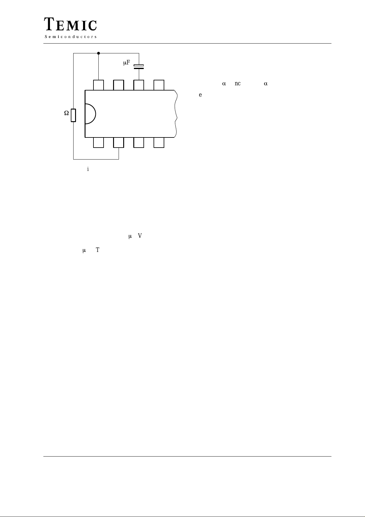
C = 1 F
10 V
R = 1 M
18
123
Figure 5. Operation delay
17 16 15
4
95 10363
Control Amplifier (Figure 2)
The integrated control amplifier with differential input
compares the set value (Pin 11) with the instantaneous
value on Pin 10 and generates a regulating voltage on the
output Pin 12 (together with the external circuitry on
Pin 12) which always tries to hold the actual voltage at the
value of the set voltages. The amplifier has a
transmittance of typically 1000 A/V and a bipolar
current source output on Pin 12 which operates with
typically ±110 A. The amplification and frequency
response are determined by R
out). For open loop operation, C
can be omitted. Pin 10 should be connected with
R
11
, C7, C8 and R11 (can be left
7
, C5, R6, R7, C7, C8 and
4
Pin 12 and Pin 8 with Pin 2. The phase angle of the
triggering pulse can be adjusted using the voltage on
Pin 11. An internal limitation circuit prevents the voltage
on Pin 12 from becoming more negative than V
+ 1 V.
16
Load Limitation
The load limitation, with standard circuitry, provides
absolute protection against overloading of the motor. the
function of the load limiting takes account of the fact that
motors operating at higher speeds can safely withstand
large power dissipations than at lower speeds due to the
increased action of the cooling fan. Similary, considerations have been made for short term overloads for the
motor which are, in practice, often required. These
finctions are not damaging and can be tolerated.
In each positive half-cycle, the circuit measures via R
the load current on Pin 14 as a potential drop across R
and produces a current proportional to the voltage on
Pin 14. This current is available on Pin 15 and is
integrated by C
a large phase angle for current flow, the voltage on C
exceeds an internally set threshold of approx. 7.3 V
. If, following high current amplitudes or
9
U211B2/ B3
(reference voltage Pin 16) then a latch is set and the load
limiting is turned on. A current source (sink) controlled
by the control voltage on Pin 15 now draws current from
Pin 12 and lowers the control voltage on Pin 12 so that the
phase angle is increased to
The simultaneous reduction of the phase angle during
which current flows causes firstly: a reduction of the
rotational speed of the motor which can even drop to zero
if the angular momentum of the motor is excessively
large, and secondly: a reduction of the potential on C
which in turn reduces the influence of the current sink on
Pin 12. The control voltage can then increase again and
bring down the phase angle. This cycle of action sets up
a “balanced condition” between the “current integral” on
Pin 15 and the control voltage on Pin 12.
Apart from the amplitude of the load current and the time
during which current flows, the potential on Pin 12 and
hence the rotational speed also affects the function of the
load limiting. A current proportional to the potential on
Pin 10 gives rise to a voltage drop across R
so that the current measured on Pin 14 is smaller than the
actual current through R
.
8
This means that higher rotational speeds and higher
current amplitudes lead to the same current integral.
Therefore, at higher speeds, the power dissipation must
be greater than that at lower speeds before the internal
threshold voltage on Pin 15 is exceeded. The effect of
speed on the maximum power is determined by the
resistor R
and can therefore be adjusted to suit each
10
individual application.
If, after the load limiting has been turned on, the
momentum of the load sinks below the “o-momentum”
set using R
, then V15 will be reduced. V12 can then in-
10
crease again so that the phase angle is reduced. A smaller
phase angel corresponds to a larger momentum of the motor and hence the motor runs up - as long as this is allowed
by the load momentum. For an already rotating machine,
the effect of rotation on the measured “current integral”
ensures that the power dissipation is able to increase with
the rotational speed. the result is: a current controlled
accelleration run-up., which ends in a small peak of accelleraton when the set point is reached. The latch of the load
limiting is simultaneously reset. The speed of the motor
is then again under control and it is capable of carrying its
full load. The above mentioned peak of accelleration
10
depends upon the ripple of actual speed voltage. A large
8
amount of ripple also leads to a large peak of
accelleration.
The measuring resistor R
ensures that the amplitude of the voltage across it does not
9
8
exceed 600 mV.
.
max
10
should have a value which
9
, via Pin 14,
TELEFUNKEN Semiconductors
Rev . A1, 29-May-96
5 (20)
Page 6
U211B2/ B3
Design Hints
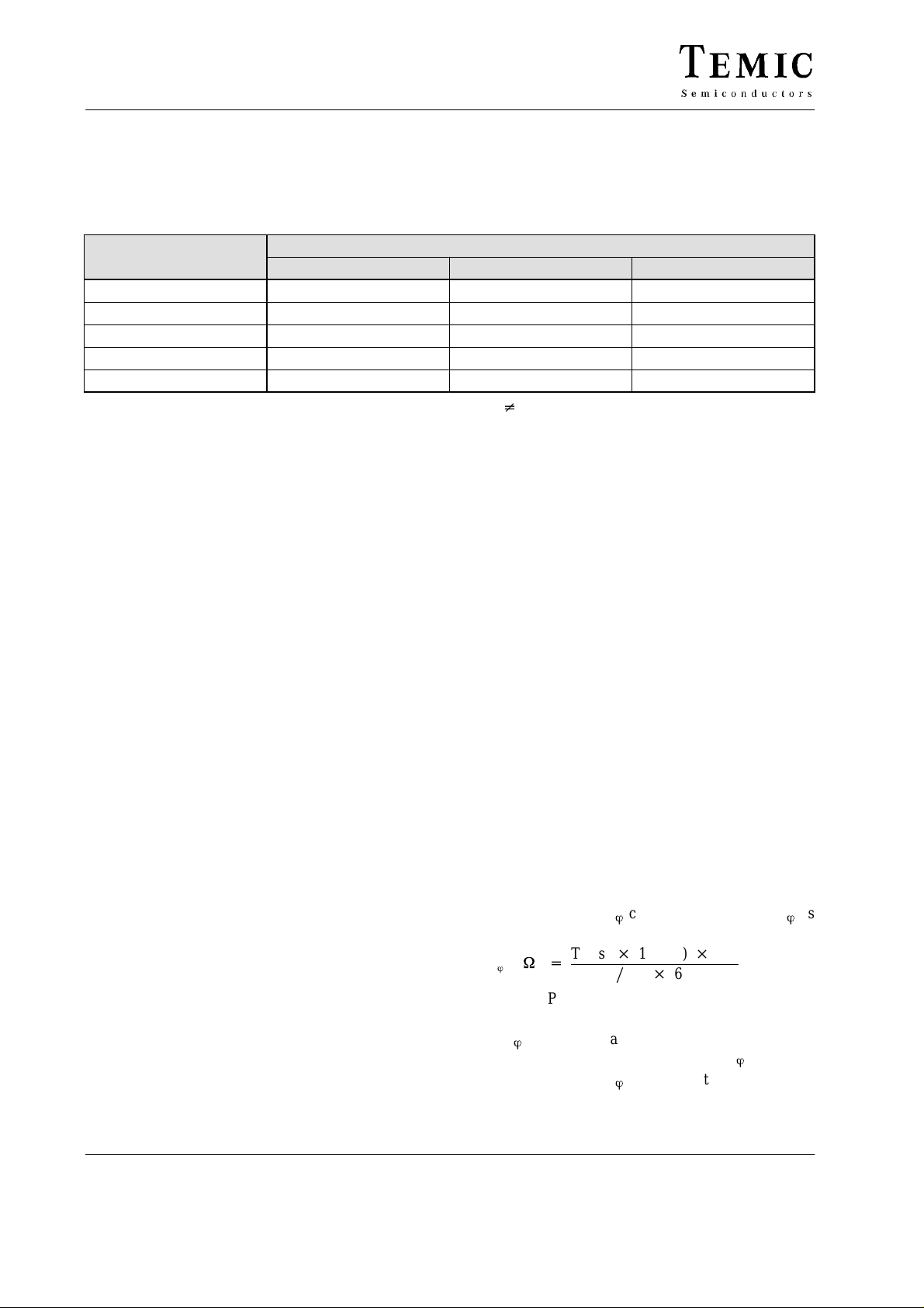
Practical trials are normally needed for the exact
determination of the values of the relevant components in
the load limiting. To make this evaluation easier, the
following table shows the effect of the circuitry on the
important parameters of the load limiting and summarises
the general tendencies.
Parameters
R
10
P
max
P
min
P
/
max
min
t
d
t
r
P
– maximum continuous power dissipation P1 = f
max
– power dissipation with no rotation P1 = f
P
min
– operation delay time
t
d
– recovery time
t
r
increases decreases n.e.
increases decreases n.e.
increases n.e. n.e.
n.e. decreases increases
n.e. increases increases
n.e – no effect
Pulse Output Stage
The pulse output stage is short circuit protected and can
typically deliver currents of 125 mA. For the design of
smaller triggering currents, the function I
= f(RGT) has
GT
been given in the data sheets in the appendix.
Automatic Retriggering
The variable automatic retriggering prevents half cycles
without current flow, even if the triac is turned off earlier
e.g. due to a collector which is not exactly centered (brush
lifter) or in the event of unsuccessful triggering. If it is
necessary, another triggering pulse is generated after a
time lapse which is determined by the repetition rate set
by resistance between Pin 5 and Pin 3 (R
maximum repetition rate (Pin 5 directly connected to
Pin 3), the next attempt to trigger comes after a pause of
and this is repeated until either the triac fires or the
4.5 t
p
half-cycle finishes. If Pin 5 is connected, then only one
trigger pulse per half-cycle is generated. Because the
value of R
repetition rate set using R
.
of C
2
determines the charging current of C2, any
5-3
is only valid for a fixed value
5-3
). With the
5-3
Component affected
R
9
n 0 0
(n)
n = 0
(n)
C
9
General Hints and Explanation of Terms
To ensure safe and trouble-free operation, the following
points should be taken into consideration when circuits
are being constructed or in the design of printed circuit
boards.
– The connecting lines from C
should be as short as possible: The connection to Pin 2
should not carry any additional high current such as
the load current. When selecting C
temperature coefficient is desirable.
– The common (earth) connections of the set-point
generator, the tacho-generator and the final
interference suppression capacitor C
converter should not carry load current.
– The tacho-generator should be mounted without
influence by strong stray fields from the motor.
– The connections from R
10
as possible.
To achieve a high noise immunity, a maximum ramp
voltage of 6 V should be used.
The typical resistance R
can be calculated from Iö as
ö
follows:
(kW)
R
ö
T(ms) 1.13(V) 10
+
CńnF) 6(V)
T = Period duration for mains frequency
(10 ms at 50 Hz)
C
= Ramp capacitor, max. ramp voltage 6 V
ö
and constant voltage drop at R
A 10% lower value of Rö (under worst case conditions)
is recommended.
to Pin 7 and Pin 2
2
and C
should be as short
5
, a low
2
of the f/V
4
3
= 1.13 V.
ö
6 (20)
TELEFUNKEN Semiconductors
Rev . A1, 29-May-96
Page 7
U211B2/ B3
V
Mains
Supply
Trigger
Pulse
Load
Voltage
Load
Current
V
GT
V
L
I
L
p
/2
t
p
p
t
pp
F
= 4.5 t
ö
3/2
p
p
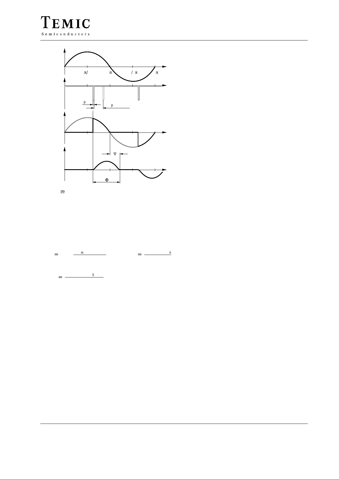
Figure 6. Explanation of terms in phase relationship
95 10716
2
p
Design Calculations for Mains Supply
The following equations can be used for the evaluation of the series resistor R
V
R
1max
P
(R1max)
+
+
0.85
(V
Mmin
Mmax
2R
2I
–V
1
tot
Smin
Smax
)
R
2
–V
where:
= Mains voltage
V
M
V
= Supply voltage on Pin 3
S
= Total DC current requirement of the circuit
I
tot
I
Smax
I
p
I
x
can be easily evaluated from the figures 20 to 22.
R
1
+ Ip + I
= I
S
x
= Current requirement of the IC in mA
= Average current requirement of the triggering pulse
= Current requirement of other peripheral components
1min
VM–V
+
2I
Smin
Smax
for worst case conditions:
1
TELEFUNKEN Semiconductors
Rev . A1, 29-May-96
7 (20)
Page 8
U211B2/ B3
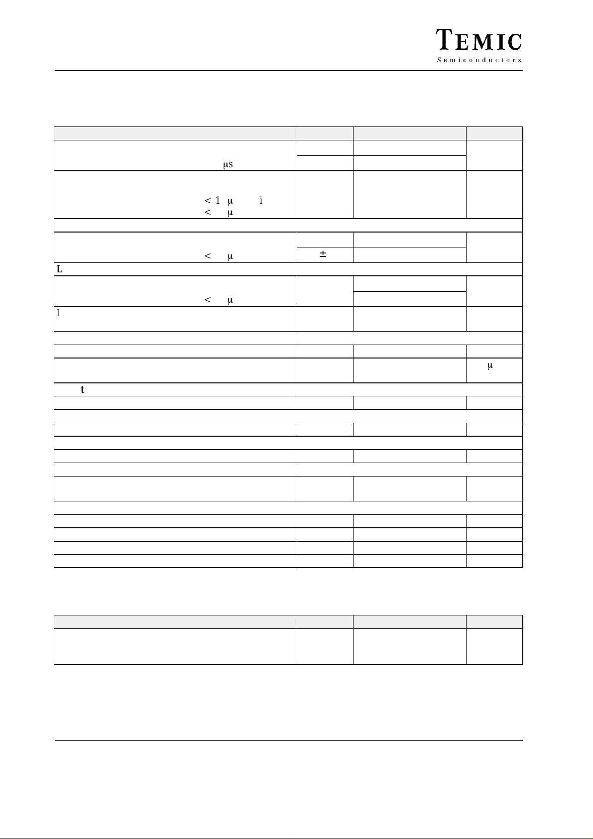
Absolute Maximum Ratings
Reference point Pin 2, unless otherwise specified
Parameters Symbol Value Unit
Current requirement Pin 3 –I
t ≤ 10 ms
Synchronization current Pin 1
Pin 17
t t 10 ms Pin 1
t t 10 ms Pin 17
f/V converter Pin 8
Input current I
t t 10 ms
Load limiting Pin 14
Limiting current, neg. half wave I
t t 10 ms
Input voltage Pin 14
Pin 15
Phase control
Input voltage Pin 12 –V
Input current Pin 12
Pin 6
Soft-start
Input voltage Pin 13 –V
Pulse output
Reverse voltage Pin 4 V
Pulse blocking
Input voltage Pin 18 –V
Amplifier
Input voltage Pin 11
Pin 9 open Pin 10
Reference voltage source
Output current Pin 16 I
Storage temperature range T
Junction temperature T
Ambient temperature range T
I
I
syncV
S
–i
s
syncI
±i
±i
I
±i
I
±V
–V
±I
–I
R
V
I
–V
o
stg
j
amb
30 mA
100
5
mA
5
I
I
35
35
3 mA
I
13
5 mA
35
i
I
I
I
I
I
1
to 0
V
16
0 to 7 V
500
1
V16 to 0 V
V
m
A
mA
VS to 5 V
I
I
V16 to 0 V
0 to V
S
V16 to 0
V
7.5 mA
–40 to +125 °C
125 °C
–10 to +100 °C
Thermal Resistance
Parameters Symbol Maximum Unit
Junction ambient DIP18
SO16 on p.c.
SO16 on ceramic
8 (20)
R
thJA
120
K/W
180
100
TELEFUNKEN Semiconductors
Rev . A1, 29-May-96
Page 9
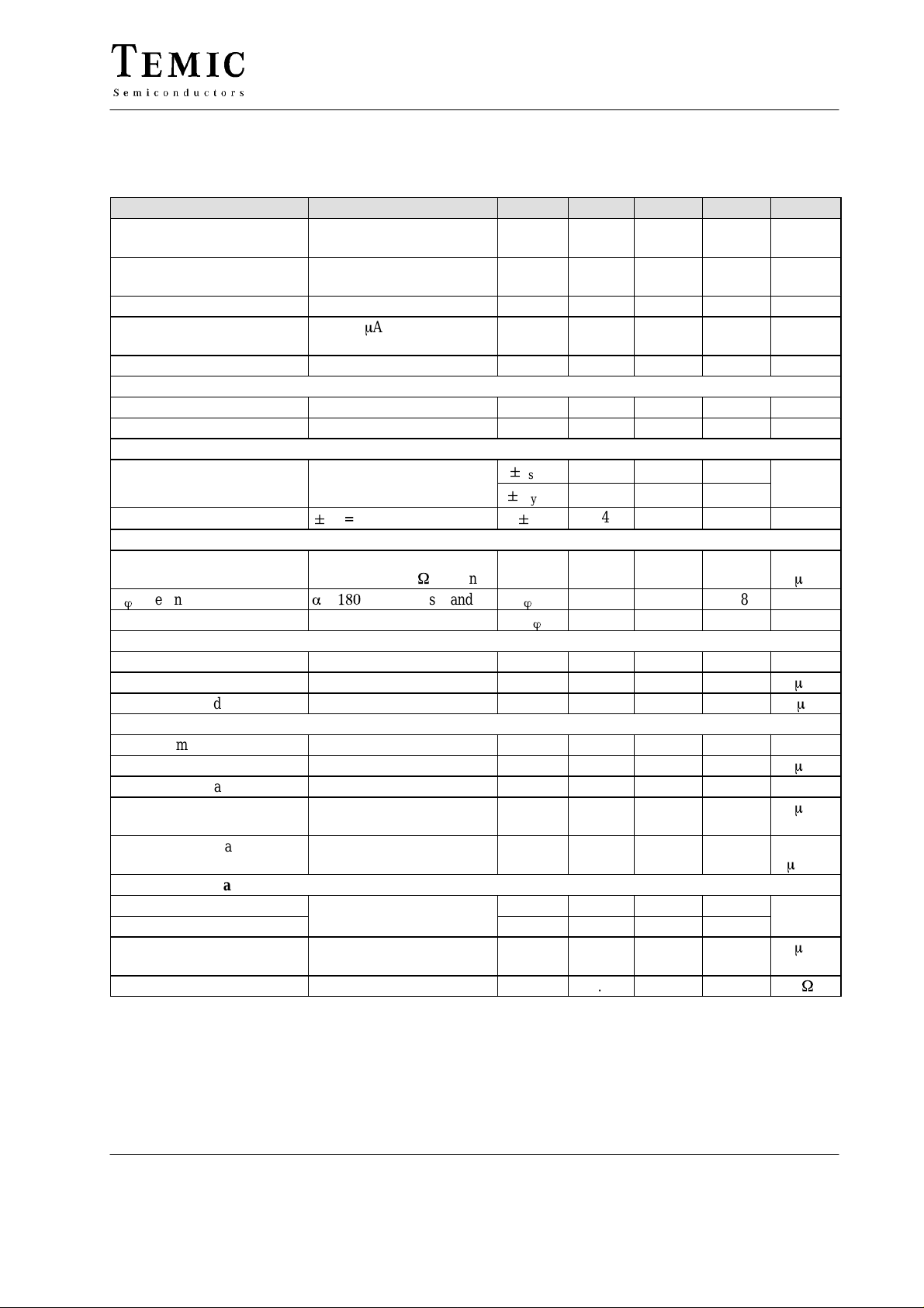
Electrical Characteristics
U211B2/ B3
–VS = 13.0 V, T
= 25°C, reference point Pin 2, unless otherwise specified
amb
Parameters Test Conditions / Pins Symbol Min. Typ. Max. Unit
Supply voltage for mains op-
Pin 3 –V
eration
Supply voltage limitation –IS = 4 mA Pin 3
= 30 mA
–I
S
DC current requirement –VS = 13.0 V Pin 3 I
Reference voltage source –IL = 10 mA Pin 16
= 5 mA
–I
L
–V
Temperature coefficient Pin 16 –TC
Voltage monitoring
Turn-on threshold Pin 3 –V
Turn-off threshold Pin 3 –V
Phase control currents
Synchronization current Pin 1
Pin 17
Voltage limitation
"
IL = 5 mA Pins 1 and 17
"
"
"
Reference ramp, figure 7
Charge current I7 = f (R6);
= 50 k to 1 MW Pin 7 I
R
6
Rö-reference voltage
a ≥ 180
°C Pins 6 and 3 V
Temperature coefficient Pin 6 TC
Pulse output, figure 18 Pin 4
Output pulse current RGT = 0, VGT = 1.2 V I
Reverse current I
Output pulse width Cϕ = 10 nF t
Amplifier
Common mode signal range Pins 10 and 11 V10,
Input bias current Pin 11 I
Input offset voltage Pins 10 and 11 V
Output current Pin 12 –I
Short circuit forward,
transmittance
Figure 14
= f(V
I
12
) Pin 12 Y
10 -11
Pulse blocking, tacho-monitoring Pin 18
Logic-on –V
Logic-off –V
Input current V
= V
18
= V
V
18
TOFF
16
= 1.25 V
Output resistance R
–V
–V
S
Ref
VRef
SON
SOFF
I
syncI
I
syncV
V
7
Ref
ö
VöRef
o
or
p
IO
10
O
+I
O
TON
TOFF
I
I
O
S
S
S
13.0 V
14.6
14.7
Limit
16.6
16.8
V
V
1.2 2.5 3.0 mA
8.6
8.3
8.9 9.2
9.1
V
0.5 mV/K
11.2 13.0 V
9.9 10.9 V
0.35 2.0 mA
0.35 2.0
I
1.4 1.6 1.8 V
1 20
m
A
1.06 1.13 1.18 V
0.5 mV/K
100 155 190 mA
0.01 3.0
80
11
V
16
–1 V
0.01 1
m
A
m
s
m
A
10 mV
75
88
f
110
120
1000
145
165
m
m
A
A/V
3.7 1.5 V
1.25 1.0
0.3 1
m
A
14.5
1.5 6 10 k
W
TELEFUNKEN Semiconductors
Rev . A1, 29-May-96
9 (20)
Page 10
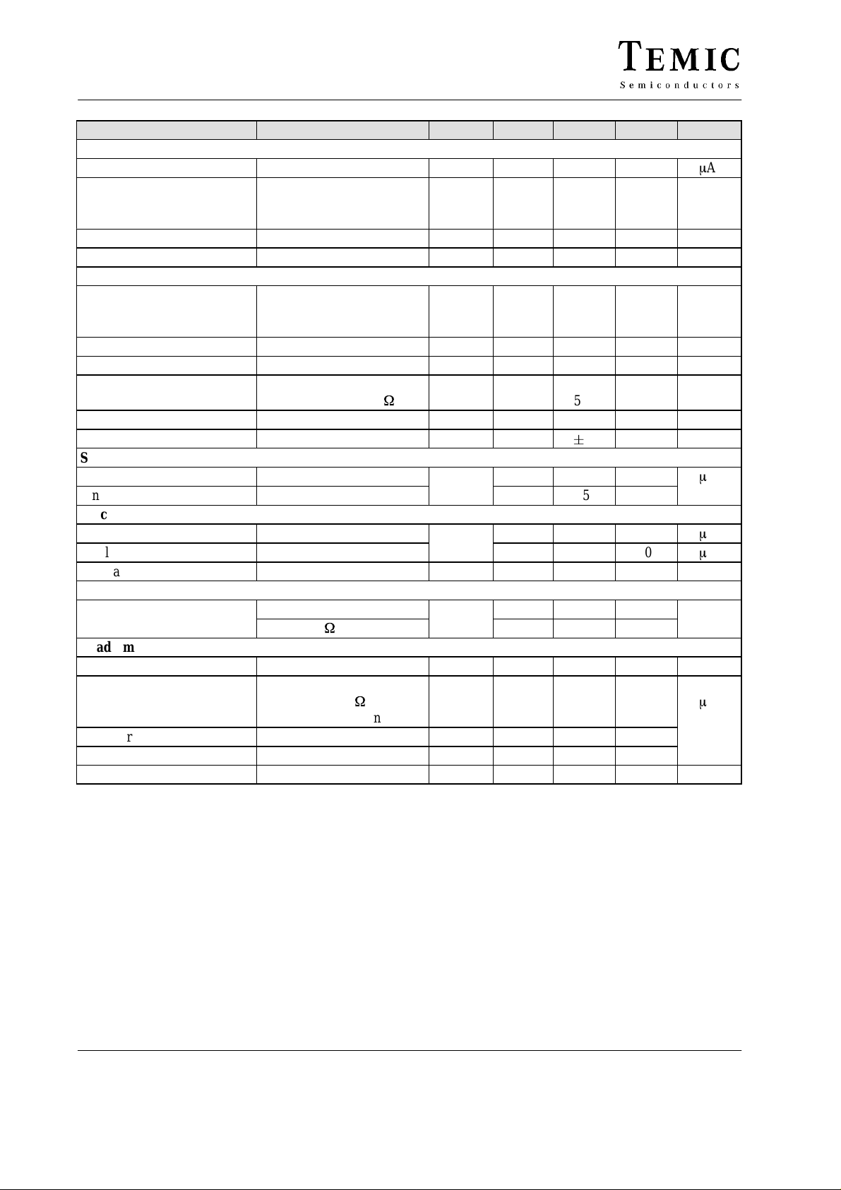
U211B2/ B3
O
m
O
p
pp20p
Frequency to voltage converter Pin 8
Input bias current I
Input voltage limitation Figure 13
= –1 mA
I
I
= +1 mA
I
I
Turn-on threshold –V
Turn-off threshold –V
Charge amplifier
Discharge current Figure 2
= 1 nF,
C
5
Pin 9
Charge transfer voltage Pins 9 to 16 V
Charge transfer gain I10/I
9
Conversion factor Figure 2
= 1 nF, R6 = 100 k
C
5
Output operating range Pins 10 to 16 V
Linearity
Soft-start, figures 8, 9, 10, 11, 12 f/v-converter non-active
Starting current V13 = V
Final current V13 = 0.5 Pin 13
f/v-converter active
Starting current V13 = V
Final current V13 = 0.5
Discharge current Restart pulse Pin 13 I
Automatic retriggering, figure 19 Pin 5
Repetition rate R
= 0 t
5-3
R
= 15 k
5-3
Load limiting, figures 15, 16, 17 Pin 14
Operating voltage range Pin 14 V
Offset current V10 = V
= V2 via 1 k
V
14
Input current V10 = 4.5 V Pin 14 I
Output current V14 = 300 mV Pin 15–16 I
Overload ON Pin 15–16 V
Pins 9 and 10 G
W
V8 = V2Pin 13 I
16,
16
Pin 13 I
W
16
Pin 14
W
Pin 15–16
UnitMax.Typ.Min.SymbolTest Conditions / PinsParameters
IB
–V
+V
TON
TOFF
I
dis
0.6 2
I
I
660
7.25
750
8.05
100 150 mV
20 50 mV
0.5 mA
ch
i
6.50 6.70 6.90 V
7.5 8.3 9.0
m
mV
V
K 5.5 mV/Hz
O
O
20 45 55
0-6 V
1 %
m
50 85 130
O
2 4 7
30 55 80
O
pp
I
I
O
0.5 3 10 mA
3 4.5 6 t
–1.0 1.0 V
5
12
m
m
m
1.0
I
O
TON
0.1
60 90 120
110 140
7.05 7.4 7.7 V
A
A
A
A
p
A
10 (20)
TELEFUNKEN Semiconductors
Rev . A1, 29-May-96
Page 11
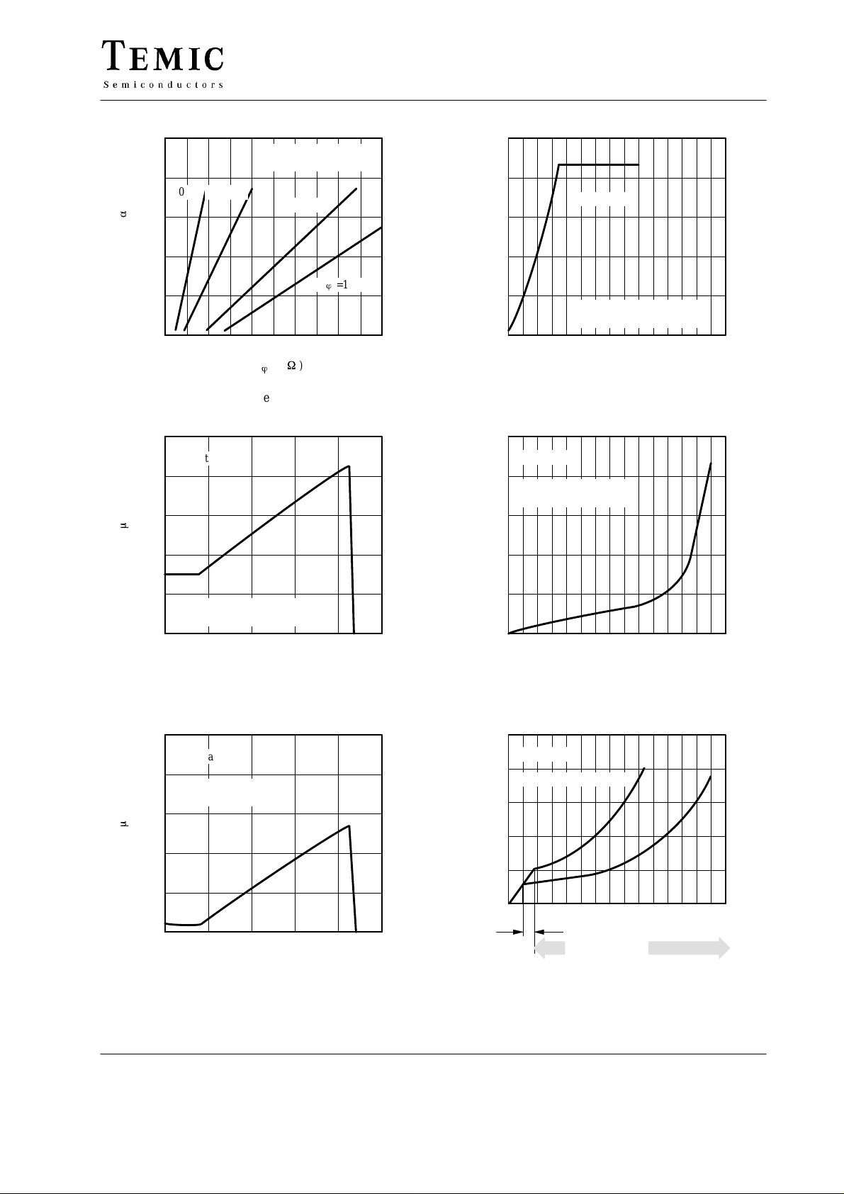
U211B2/ B3
240
200
°
160
120
Phase Angle ( )
80
0
95 10302
100
80
60
13
I ( A )
40
Phase Control
Reference Point Pin 2
10nF 4.7nF
2.2nF
C
=1.5nF
/t
0 0.2 0.4 0.6 0.8
R ( M )
Figure 7.
Soft Start
1.0
13
V ( V )
95 10305
13
V ( V )
10
8
6
4
2
0
10
Soft Start
8
f/V-Converter Active
Reference Point Pin 16
6
4
Soft Start
f/V-Converter Non Active
Reference Point Pin 16
t=f
(C3)
Figure 10.
95 10303
13
I ( A )
95 10304
20
f/V-Converter Non Active
Reference Point Pin 16
0
02468
V13 ( V )
Figure 8.
100
Soft Start
80
f/V-Converter Active
Reference Point Pin 16
60
40
20
0
02468
V13 ( V )
Figure 9.
2
0
10
95 10306
t=f
(C3)
Figure 11.
10
Soft Start
8
Reference Point Pin 16
6
13
V ( V )
4
2
0
t=f
10
Motor Standstill ( Dead Time )
Motor in Action
(C3)
95 10307
Figure 12.
TELEFUNKEN Semiconductors
Rev . A1, 29-May-96
11 (20)
Page 12
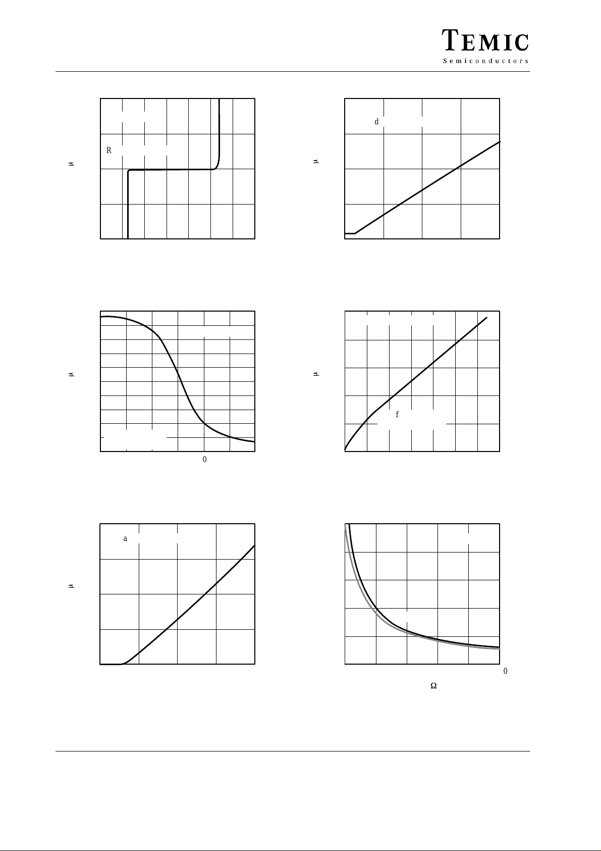
U211B2/ B3
500
f/V–Converter
250
Reference Point Pin 2
m
0
8
I ( A )
–250
–500
–10 –8 –6 –4 –2
95 10308
V8 ( V )
Figure 13.
100
50
m
0
12
I ( A )
–50
Reference Point
–100
for I
= –4V
12
–300 –200 –100 0 200
95 10309
V
10–11
02
Control Amplifier
100
( V )
300
200
Load Limit Control
150
m
100
14–2
I ( A)
50
0
4
95 10311
024 6
V
(V)
10–16
8
Figure 16.
250
Load current detection
200
150
m
15–16
100
I ( A )
95 10312
50
V
10=V16
0
0 100 200 300 400
I15=f ( V
V
Shunt
14–2
)
( mV )
500 600
700
m
12–16
–I ( A)
95 10310
12 (20)
Figure 14.
200
Load Limit Control
150
100
50
0
024 6
V
( V )
15–16
Figure 15.
Figure 17.
100
Pulse Output
80
60
GT
I ( mA )
40
1.4V
VGT=0.8V
20
0
8
95 10313
0 200 400 600 800
RGT ( W )
1000
Figure 18.
TELEFUNKEN Semiconductors
Rev . A1, 29-May-96
Page 13
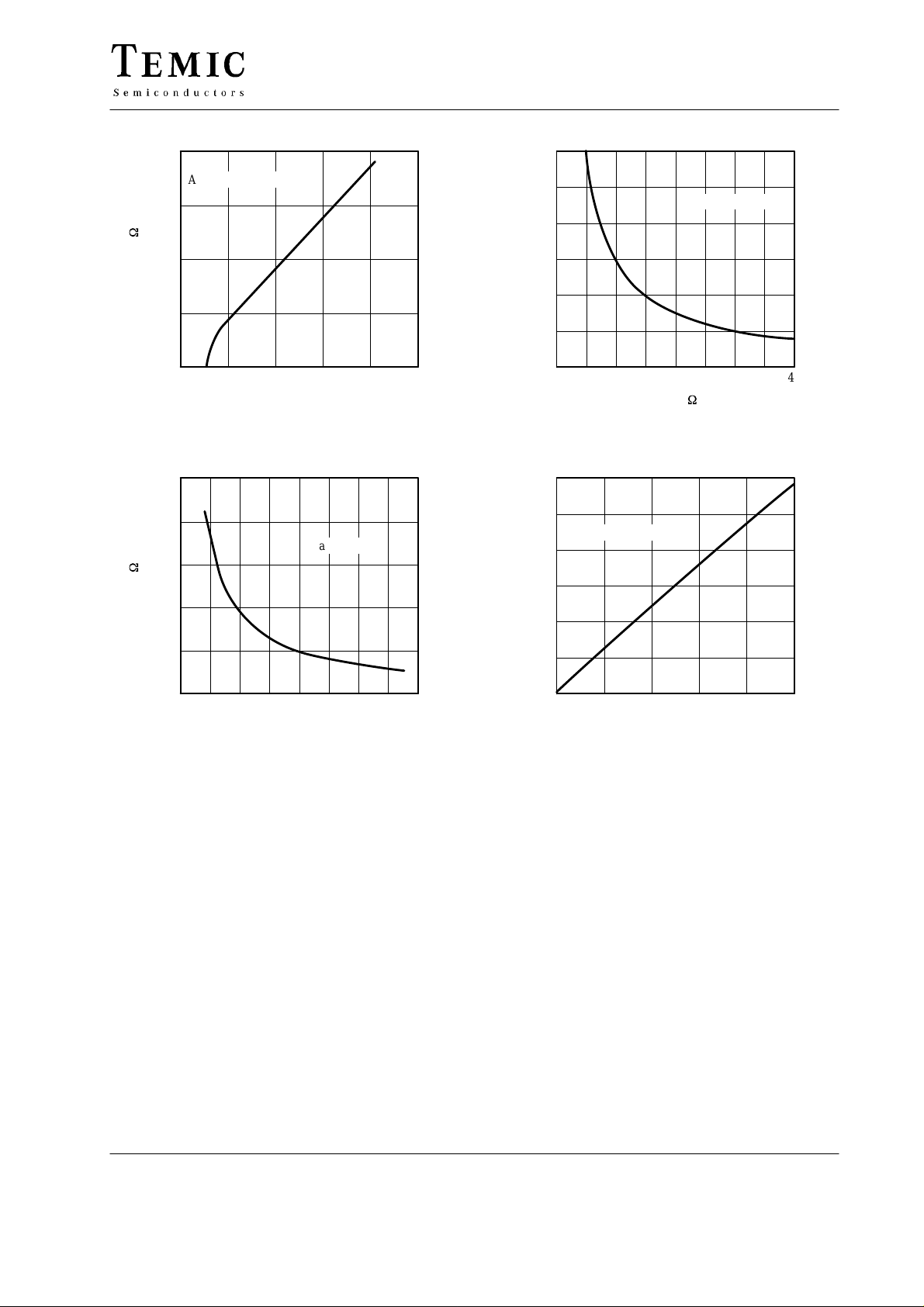
U211B2/ B3
20
15
W
10
5–3
R ( k )
5
0
95 10314
50
40
30
W
1
R ( k )
20
Automatic Retriggering
0 6 12 18 24
tpp/t
p
Figure 19.
Mains Supply
6
5
Mains Supply
4
3
(R1)
P ( W )
2
1
95 10316
0
0102030
( kW )
R
1
40
30
Figure 21.
6
5
Mains Supply
P ( W )
4
3
(R1)
2
95 10315
10
0
04812
I
( mA )
tot
Figure 20.
1
95 10317
0
03 6 912
I
( mA )
tot
15
16
Figure 22.
TELEFUNKEN Semiconductors
Rev . A1, 29-May-96
13 (20)
Page 14
U211B2/ B3
9
R
11
C
BZX55
F
m
2.2
10
C
R
W
100 k
8
C
F
m
4.7
9
C
W
470 k
F
m
2.2
10 V
6
220 nF
10 V
T1
100 nF
6
C
14
R
11
R
R
C
F
m
2.2
W
10 k
W
47 k
15
31
R
3
10 V
16
R
W
250 k
W
1 M
T2
voltage
Set speed
7
C
W
47 k
10 V
F
m
2.2 /
W
220 k
W
13
R
47 k
10
11
13 12
14
W
7
R
15 k
5
C
4
220 nF
680 pF
C
9
W
5
1 k
8
7
R
56
R
/t
ö
C
2
ö
C
R
2
W
2.2 nF
Speed sensor
1 M
U211B2
4
S
16 15
17
18
3
R
1
D
1N4004
W
10
R
2.2 k
M
–V
GND
12
123
R
W
1.5 W
18 k
1
R
R
W
4
470 k
W
180
F
m
22
C
25 V
1
W
= 3 x 11 m
R
1 W
8
95 10364
L
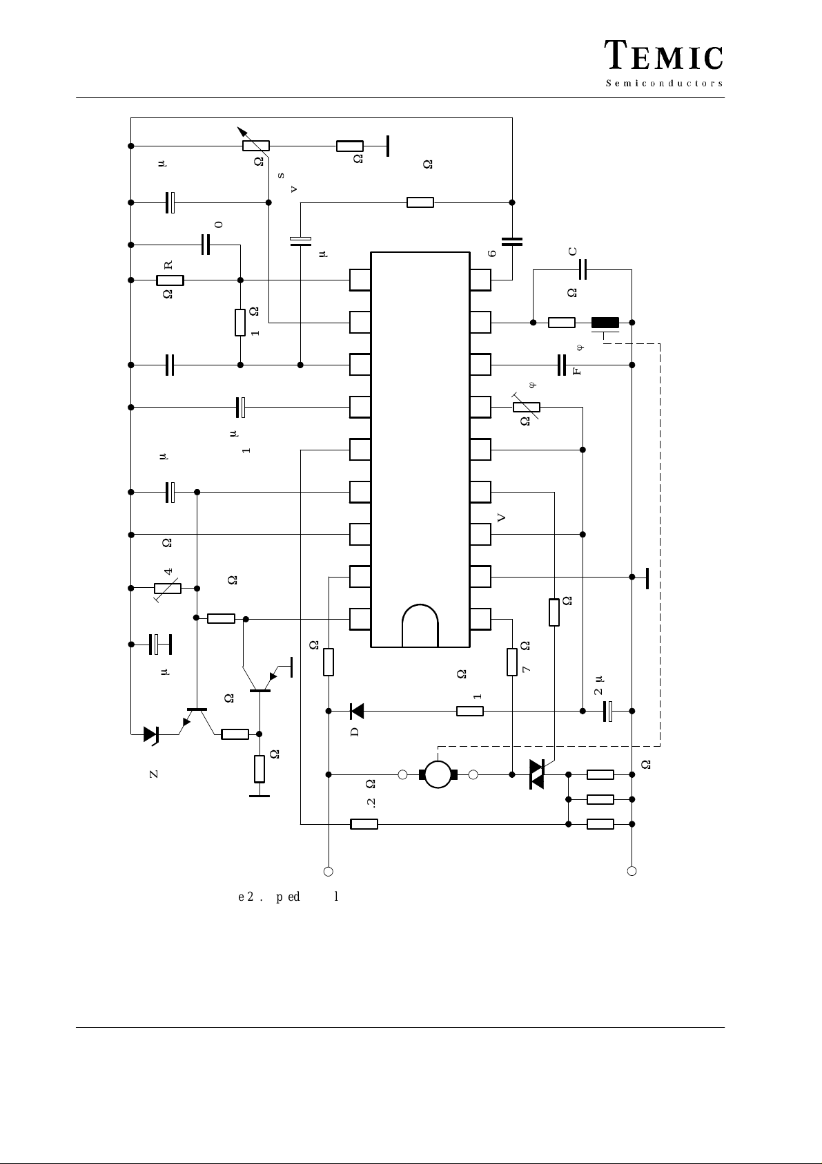
Figure 23. Speed control, automatic retriggering, load switch-off, soft start
The switch-off level at maximum load shows in principle
the same speed dependency as the original version (see
figure 2), but when reaching the maximum load, the
motor is switched off completely.
14 (20)
230 V~
N
This function is effected by the thyristor (formed by T
and T
which ignites when the voltage at Pin 15 reaches
2)
typ. 7.4 V (Reference point Pin 16). The circuit is thereby
switched into the “stand-by” over the release Pin 18.
TELEFUNKEN Semiconductors
Rev . A1, 29-May-96
1
Page 15
U211B2/ B3
F
m
2.2
10
C
R
10 V
6
6
C
31
R
100 nF
W
250 k
voltage
Set speed
7
C
W
W
100 k
11
R
1 M
220 nF
8
C
F
m
4.7
10 V
9
C
F
11
m
C
2.2
C
F
m
2.2
3
10 V
F
m
2.2 /10 V
W
13
R
47 k
10
11
13 12
14
W
7
15 k
R
5
C
4
220 nF
680 pF
C
9
W
5
1 k
8
567
R
/t
ö
C
2
ö
C
R
2
W
R
2.2 nF
Speed sensor
1 M
U211B2
S
16 15
GND –V
17
W
12
R
180
W
4
R
470 k
F
m
22
1
C
25 V
W
1 W
= 3 x 11 m
8
R
M
W
18 k
1
R
1234
1.5 W
18
T1
W
14
R
10 k
W
220 k
3
R
T2
1
D
10
R
1N4004
W
2.2 k
W
16
R
47 k
W
9
R
470 k
W
15
R
33 k
BZX55
95 10366
L
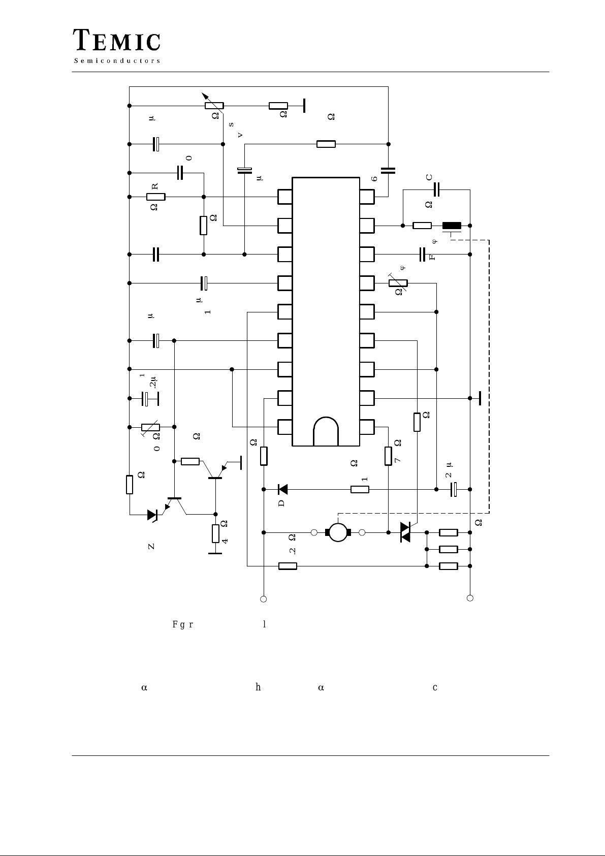
Figure 24. Speed control, automatic retriggering, load switch-off, soft-start
The maximum load regulation shows the principle in the
same speed dependency as the original version (see
figure 2). When reaching the maximum load, the control
unit is turned to
, adjustable with R2. Then only I
a
max
flows. This function is effected by the thyristor, formed
by T
and T
1
which ignites as soon as the voltage at Pin 15
2
reaches ca. 6.8 V (Reference point Pin 16). The potential
TELEFUNKEN Semiconductors
Rev . A1, 29-May-96
230 V~
N
at Pin 15 is lifted and kept by R
over the internally
14
operating threshold whereby the maximum load
regulation starts and adjusts the control unit constantly to
(IO), inspite of a reduced load current. The motor
a
O
max
shows that the circuit is still in operation by a quiet
buzzing noise.
15 (20)
Page 16
U211B2/ B3
F
m
2.2
10
C
R
W
68 k
8
C
R
9
C
10 V
6
9
220 nF
W
1 M
F
m
4.7
100 nF
6
C
W
W
31
R
voltage
250 k
Set speed
7
C
W
11
R
1.5 M
3
C
F
m
2.2
10 V
13
R
47 k
F
m
2.2 /10 V
10
11
13 12
14
W
7
R
22 k
5
C
1 nF
4
C
220 nF
9
W
5
1 k
ö
R
W
1 M
R
Speed sensor
/t
ö
C
2
C
2.2 nF
8
7
2
R
56
U211B2
4
S
16 15
–V
95 10365
F
W
1 M
m
1 /10 V
W
220 k
11
C
22 nF
17
12
18
3
R
1
D
123
R
W
18 k
1.5 W
1
R
R
W
4
470 k
1N4004
M
GND
W
10
R
1 k
L
230 V~
N
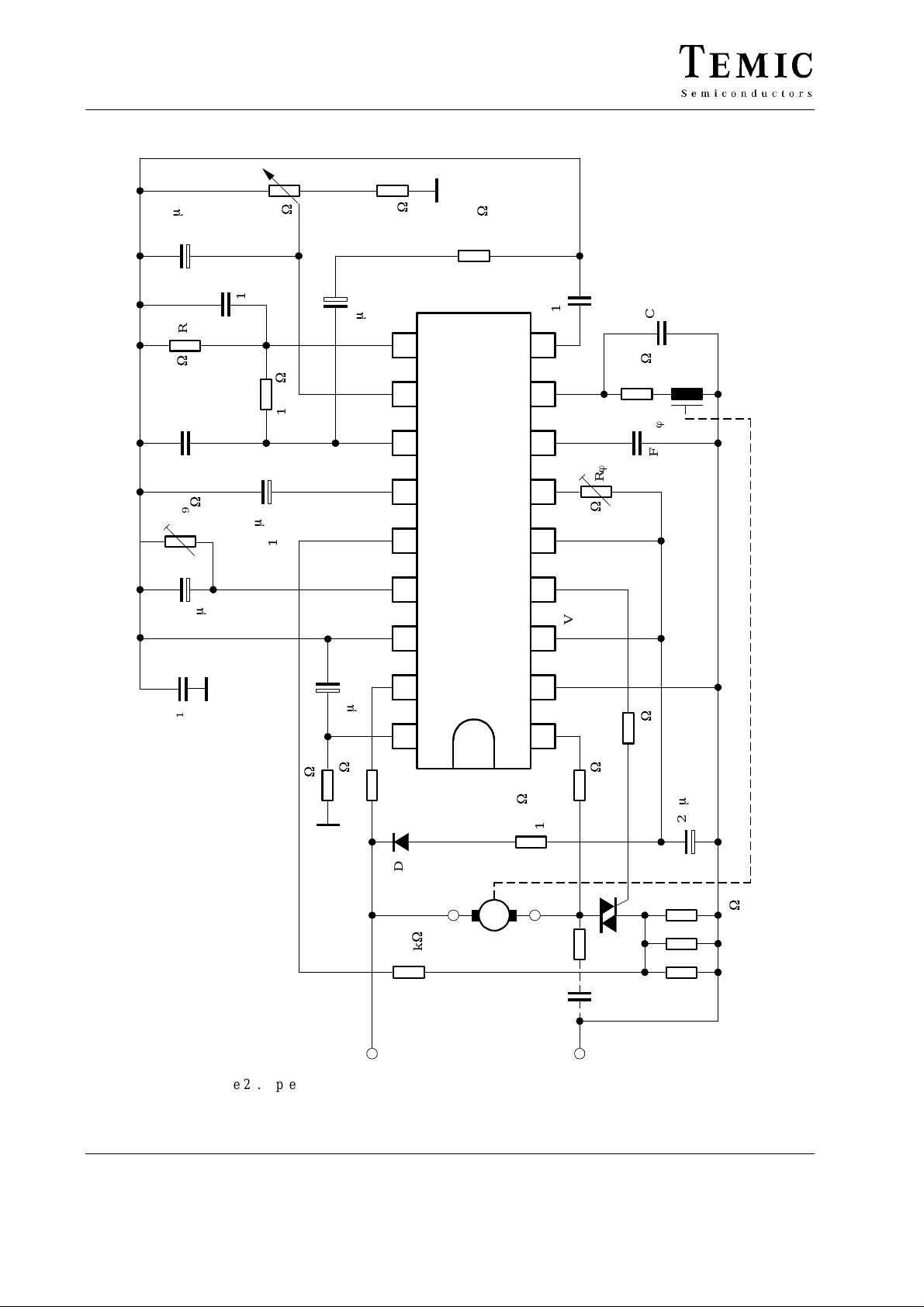
Figure 25. Speed control, automatic retriggering, load limiting, soft-start, tacho control
W
220
F
m
22
1
C
25 V
W
= 3 x 11 m
R
1 W
8
16 (20)
TELEFUNKEN Semiconductors
Rev . A1, 29-May-96
Page 17
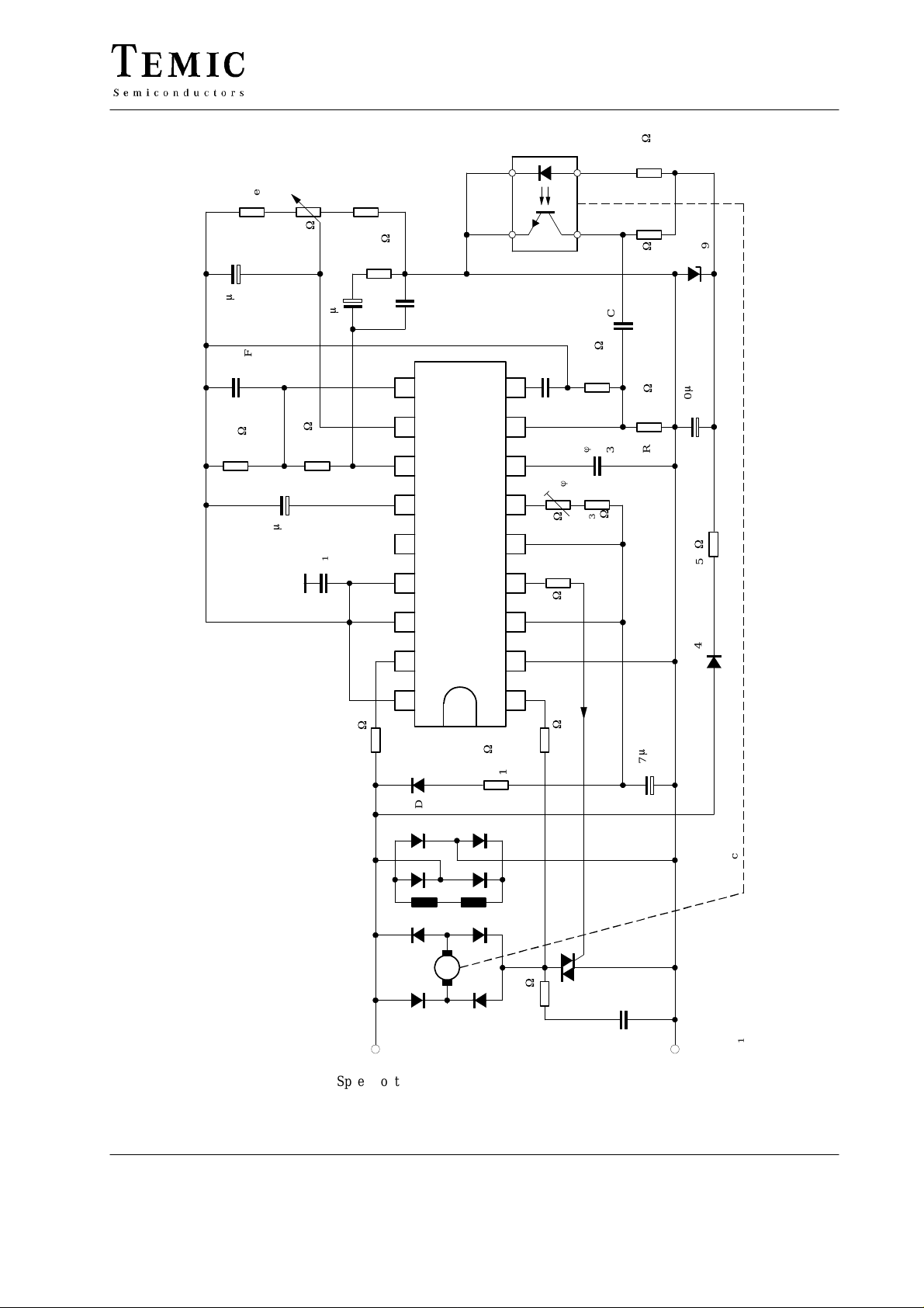
U211B2/ B3
W
470
min
18
Set speed
R
W
31
R
13
C
F
m
4.7
10 V
100 k
10 V
F
m
10
13
R
C
max
Set speed
W
11
R
16 k
7
8
C
CNY 70
470 nF
W
4
C
220 nF
W
8
R
47 k
W
470 k
7
R
3
C
F
m
2.2
10 V
11
C
22 nF
10
11
13 12
14
U211B2
9
6
C
8
7
2
R
56
4
S
16 15
W
18 k
R
1.5 W
1
GND –V
123
5
R
W
220 k
17
18
4
R
1N4004
1
D
680 pF
ö
R
W
1 M
6
R
W
100
W
470 k
R
/t
ö
C
2
C
3
R
= 50 mA
GT
I
220 k
9
5
C
3.3 nF
W
4.7 k
R
R
W
100
470 nF
W
1.5 k
R
F
m
47
1
C
16
17
10
25 V
BZX55
3
Z
F
m
100
10 V
10
C
/ 8 W
W
3.5 k
1N4004
C9V1
15
R
2
D
Figure 26. Speed control with reflective opto coupler CNY70 as emitter
TELEFUNKEN Semiconductors
Rev . A1, 29-May-96
1
L
all diodes BYW83
ca 220 Pulses / Revolution
2
L
M
W
14
100
230 V~
R
150 nF
12
C
250 V~
95 10687
17 (20)
Page 18
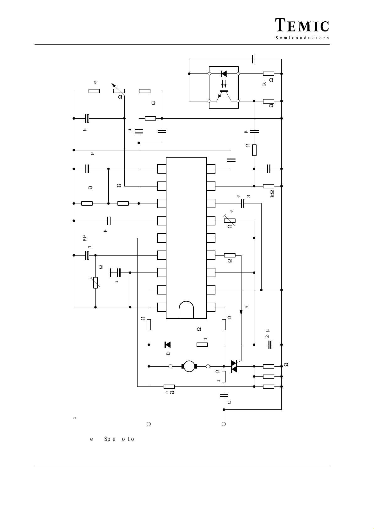
U211B2/ B3
9 V
min
14
Set speed
R
W
31
R
3
F
m
2.2
10 V
C
W
820 k
R
11
220 k
11
22 nF
F
m
10
10
C
F
m
47
10 V
6
C
470 nF
W
6
R
82 k
C
F
m
4.7
10 V
9
C
W
220 k
9
R
13
Set speed
R
C
max
W
18
R
470
CNY 70
W
7
R
16 k
F
m
8
7
470 nF
C
1
W
5
C
10
11
9
8
7
2
R
14 13 12
56
U211B2
ö
R
W
1 M
12
R
680 pF
/t
ö
C
C
10 k
3.3 nF
2
W
17
R
33 k
13
C
16
R
1 nF
4
C
5
W
R
2.2 k
4
W
S
100
17 16 15
GND –V
18 (20)
W
10 k
1
R
123
1.1 W
= 50 mA
GT
W
220 k
I
F
m
22
25 V
1
C
4
R
W
110 k
18
3
R
1N4004
1
D
M
W
100
W
10
95 10688
R
1.1 k
150 nF
250 V~
12
C
230 V~
Figure 27. Speed control, max. load control with reflective opto coupler CNY70 as emitter
TELEFUNKEN Semiconductors
W
= 3 x 0.1
8
R
Rev . A1, 29-May-96
Page 19
U211B2/ B3
The circuit is designed as a speed control on the
reflection-coupled principle with 4 periods per revolution
and a max. speed of 30.000 rpm. The separation of the
coupler from the rotating aperture should be 1 mm
approximately. In this experimental circuit, the power
supply for the coupler was provided externally because of
the relatively high current consumption.
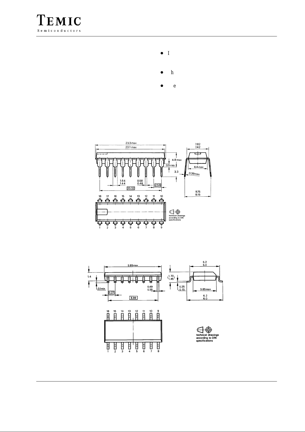
Dimensions in mm
Package: DIP18 – U211B2
Instructions for adjusting:
D
In the initial adjustment of the phase-control circuit,
should be adjusted so that when R
R
2
= 0 and R
14
in min. position, the motor just turns.
D
The speed can now be adjusted as desired by means of
between the limits determined by R13 and R14.
R
31
D
The switch-off power of the limit load control can be
set by R
. The lower R9, the higher the switch-off
9
power.
31
are
Package: SO16 – U211B3
94 8877
94 8875
TELEFUNKEN Semiconductors
Rev . A1, 29-May-96
19 (20)
Page 20

U211B2/ B3
Ozone Depleting Substances Policy Statement
It is the policy of TEMIC TELEFUNKEN microelectronic GmbH to
1. Meet all present and future national and international statutory requirements.
2. Regularly and continuously improve the performance of our products, processes, distribution and operating systems
with respect to their impact on the health and safety of our employees and the public, as well as their impact on
the environment.
It is particular concern to control or eliminate releases of those substances into the atmosphere which are known as
ozone depleting substances (ODSs).
The Montreal Protocol ( 1987) and its London Amendments (1990 ) intend to severely restrict the use of ODSs and
forbid their use within the next ten years. Various national and international initiatives are pressing for an earlier ban
on these substances.
TEMIC TELEFUNKEN microelectronic GmbH semiconductor division has been able to use its policy of
continuous improvements to eliminate the use of ODSs listed in the following documents.
1. Annex A, B and list of transitional substances of the Montreal Protocol and the London Amendments respectively
2. Class I and II ozone depleting substances in the Clean Air Act Amendments of 1990 by the Environmental
Protection Agency (EPA) in the USA
3. Council Decision 88/540/EEC and 91/690/EEC Annex A, B and C (transitional substances) respectively.
TEMIC can certify that our semiconductors are not manufactured with ozone depleting substances and do not contain
such substances.
We reserve the right to make changes to improve technical design and may do so without further notice.
Parameters can vary in different applications. All operating parameters must be validated for each customer
application by the customer. Should the buyer use TEMIC products for any unintended or unauthorized
application, the buyer shall indemnify TEMIC against all claims, costs, damages, and expenses, arising out of,
directly or indirectly, any claim of personal damage, injury or death associated with such unintended or
unauthorized use.
20 (20)
TEMIC TELEFUNKEN microelectronic GmbH, P.O.B. 3535, D-74025 Heilbronn, Germany
Telephone: 49 (0)7131 67 2831, Fax number: 49 (0)7131 67 2423
TELEFUNKEN Semiconductors
Rev . A1, 29-May-96
 Loading...