

Page 1
RGB Video Amplifier System for Monitors
Description
The U2203B-A is a wideband video amplifier IC system
especially designed for use in high-resolution RGB monitors. The IC includes three well matched video
amplifiers, three gated differential amplifiers for black-
Features
D
3 channels, high bandwidth (90 MHz @ –3 dB)
D
Matched attenuators for contrast control
D
Black-level clamping for brightness control
Vs1
1
level clamping and brightness control and the function for
simultaneously contrast control. Separate adjustment of
the maximum gain of each channel is also possible.
D
Independent gain control of each amplifier
D
ESD protection according to MIL-STD. 883
U2203B
28 Vs1
CONTRAST CAP
CONTRAST CAP23
R VIDEO IN
R CLAMP CAP
G VIDEO IN
GROUND
G CLAMP CAP
B VIDEO IN
B CLAMP CAP
Vin REF
CONTRAST1112
4
5
6
7
8
9
10
2.4V
REF
CONTRAST
CONTROL
SUPPLY
REG.
RED
GREEN
BLUE
1k
40
90
1k
40
90
1k
40
90
27 R DRIVE
26 R CLAMP (–)
25 R VIDEO OUT
24 R CLAMP (+)
23 Vs2
22 G DRIVE
21 G CLAMP (–)
20 G VIDEO OUT
19 G CLAMP (+)
18 B DRIVE
17 B CLAMP (–)
13
Vs1
CLAMP GATE
1.4V
REF
14
TELEFUNKEN Semiconductors
Rev . A2, 27-Jan-97
U2203B
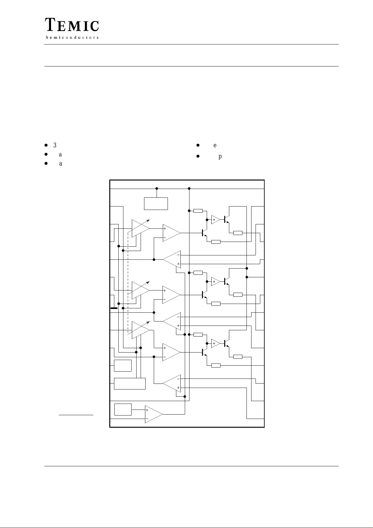
Figure 1. Block diagram
95 10749
16 B VIDEO OUT
15 B CLAMP (+)
1 (7)
Page 2
U2203B
Pin Description
V
S1
C
contr
C
contr
V
in, R
C
clamp, R
V
in, G
GND
C
clamp, G
V
in, B
C
clamp, B
V
Bias
V
contr
V
S1
V
Gate
1
2
3
4
5
6
7
8
9
10
11
12
13
14
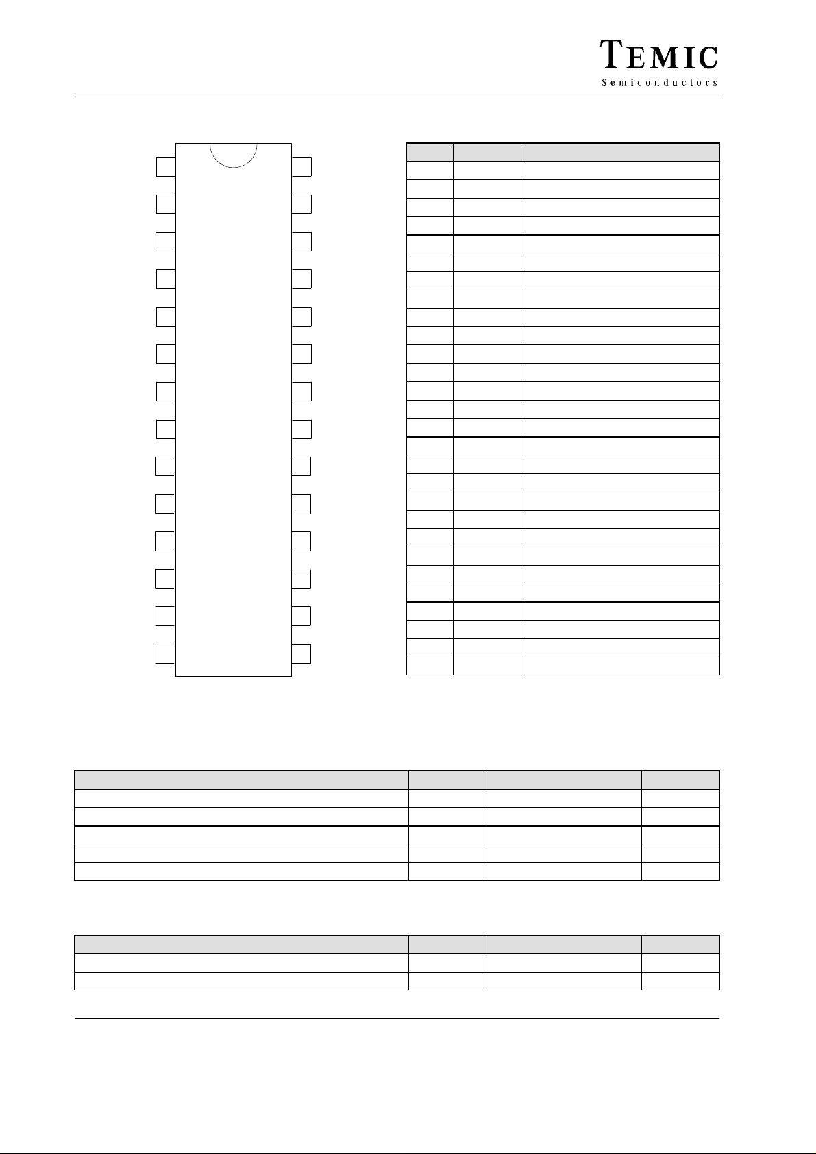
Figure 2. Pinning
96 12388
28
27
26
25
24
23
22
21
20
19
18
17
16
15
V
R
V
V
V
V
R
V
V
V
R
V
V
V
S1
R
R–
out, R
R+
S2
G
G–
out, G
G+
B
B–
out, B
B+
Pin Symbol Function
1 V
2 C
3 C
4 V
5 C
clamp, R
6 V
contr
contr
in, R
in, G
S1
Supply voltage
Contrast cap.
Contrast cap.
Video input (R)
Clamp cap. (R)
Video input (G)
7 GND Ground
8 C
clamp, G
9 V
10 C
clamp, B
11 V
12 V
13 V
14 V
15 V
16 V
17 V
18 R
19 V
20 V
21 V
22 R
23 V
24 V
25 V
26 V
27 R
28 V
in, G
Bias
contr
Gate
B+
in, B
B–
G+
out, G
G–
R+
out, R
R–
Clamp cap. (G)
Video input (B)
Clamp cap. (B)
Bias voltage (RGB-inputs)
Contrast control
Supply voltage
S1
Inverted clamp gate
Clamp amplifier (B+)
Video output (B)
Clamp amplifier (B–)
Drive resistor (B)
B
Clamp amplifier (G+)
Video output (G)
Clamp amplifier (G–)
Drive resistor (G)
G
Supply voltage (outputs)
S2
Clamp amplifier (R+)
Video output (R)
Clamp amplifier (R–)
Drive resistor (R)
R
Supply voltage
S1
Absolute Maximum Ratings
Parameters Symbol Value Unit
Supply voltage Pins 1, 13, 28 and 23 V
Input voltage at all other pins V
Video output current Pins 16, 20 and 25 I
Junction temperature T
Storage temperature range T
Operating Range
Parameters Symbol Value Unit
Ambient temperature range T
Supply voltage range Pins 1, 13, 23 and 28 VS2, V
2 (7)
amb
V
stg
S
in
13.5 V
0 toV
S
V
28 mA
j
125 °C
–40 to 125 °C
0 to 80 °C
S1
11.0 to 13.0 V
TELEFUNKEN Semiconductors
Rev . A2, 27-Jan-97
Page 3
U2203B
p
Thermal Resistance
Parameters Symbol Value Unit
Junction ambient (DIP28) R
thJA
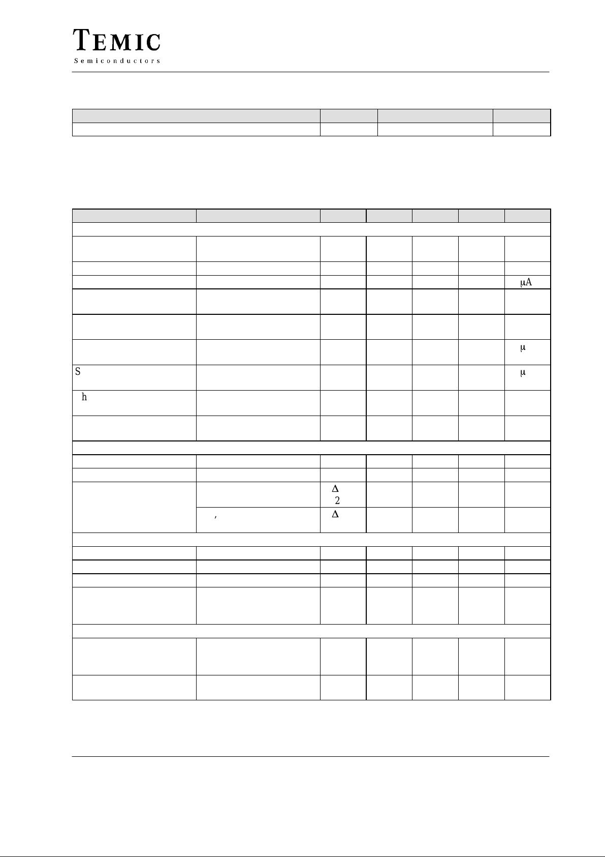
Electrical Characteristics
Test conditions unless otherwise specified, reference point Pin 7, T
= VS2 = 12 V, V12 = 6 V (contrast); V14 = 0 V (inv. gating); V15 = V19 = V24 = 2 V (brightness)
V
S1
Parameters Test Conditions / Pins Symbol Min. Typ. Max. Unit
DC-values
Supply current VS1 only,
Pins 1, 13 and 28
Input bias voltage Pin 11 V
Input bias current Pins 4, 6 and 9 I
Switching voltage gating
Pin 14 VG “L” 0.8 1.3 V
“on”
Switching voltage gating
Pin 14 VG “H” 1.5 2.0 V
“off”
Switching current gating
”on”
Switching current gating
”off”
Charge current clamping
capacitor
Discharge current clamping
capacitor
Video outputs, V
O
Low level V
High level V
Output offset between two
V14 = 0.8 V
Pin 14
V14 = 2.0 V
Pin 14
V
= 0 V
5,8,10
Pins 5, 8 and 10
V
= 5 V
5,8,10
Pins 5, 8 and 10
Pins 16, 20 and 25
= 0 V V
5,8,10
= V
5,8,10
S
V15, V19, V24 = 2 V
amplifiers
V15, V19, V24 = 4 V
Video gain V15 = V19 = V24 = 4 V (brightness); fIN = 1 MHz
Maximum video gain V12 = 12 V G
Middle video gain V12 = 5 V GV
Dynamic gain range GVD 50 dB
Video gain match
(any 2 outputs)
V12 = 12 V
= 5 V
V
12
= 2.2 V 1)
V
12
GVM
GVM
GVM
Video bandwidth
unpeaked (C = 0 pF)
optimal peaking
V12 = 12 V (f
= 12 V (f
V
12
–3dB
–3dB
)
)
(C = 27 pF)
Video cross talk fIN = 10 kHz
= 10 MHz
f
IN
CT
CT
= 25°C,
amb
I
S1
inREF
inREF
2.3 2.5 V
1 5 10
IG “L” –1 –0.01
IG “H” 5 8
ICL+ 0.8 1.0 1.2 mA
ICL– –1.2 –1.0 –0.8 mA
O“L”
V
O“H”
D
V
O
8.0 8.6 V
(2 V)
D
V
O
(4 V)
Vmax
mid
max
mid
–30
16.0 17.7 dB
BWV
BWV
P
10kHz
10MHz
–50
46 K/W
60 70 mA
0.8 1.0 V
±50 mV
±50 mV
8.5 dB
±0.1
±0.1
±0.3
65
90
MHz
MHz
–47
m
m
m
dB
dB
dB
dB
dB
A
A
A
1) Measured 30 dB below maximum gain
TELEFUNKEN Semiconductors
3 (7)
Rev . A2, 27-Jan-97
Page 4
U2203B
VS(+12V)
R Video in
75
W
G Video in
75
W
B Video in
75
W
100 mF
5 mF
5 mF
5 mF
5 mF
10 k
100 nF
W
10 k
W
10 k
100 nF
100 nF
100 nF
W
100 nF
1
2
3
4
5
6
7
9
10
U2203B
28
27
26
25
24
23
22
218
20
19
51
51
W
100
W
C
R Clamp (–)
To cascade
driver (R)
390
W
100 nF
W
C
390
W
91
100
W
W
G Clamp (–)
To cascade
driver (G)
Black level
gate I/P
93 7632
4 (7)
10 k
W
100 nF
11
12
13
100 nF
14
10 k
W
Contrast
control
0 ... 12 V
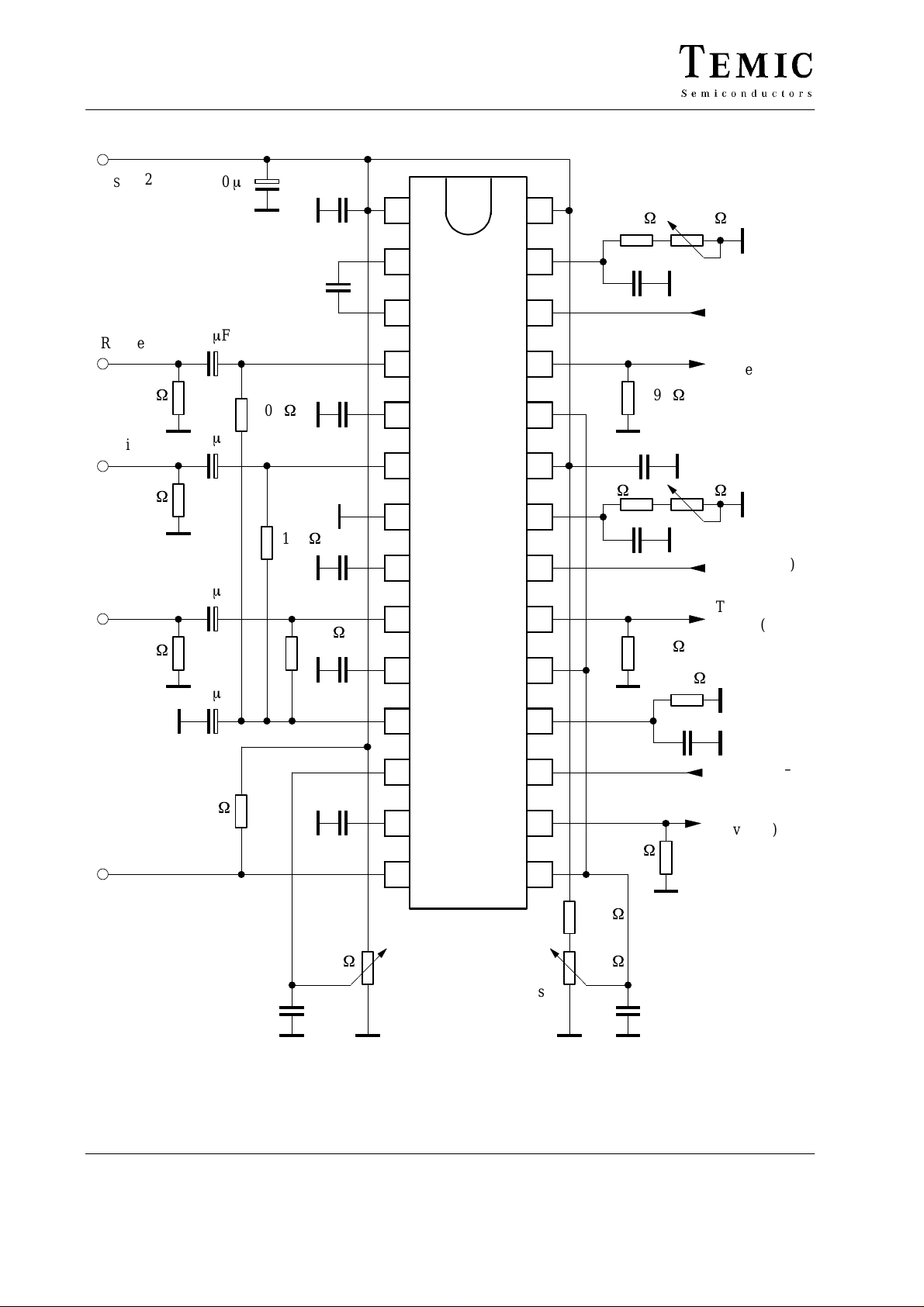
Figure 3. Typical application circuit
18
17
16
15
Black level
(brightness)
control
C
G Clamp (–)
To cascade
driver (B)
390
W
10 k
W
10 k
W
10 nF
TELEFUNKEN Semiconductors
Rev . A2, 27-Jan-97
Page 5
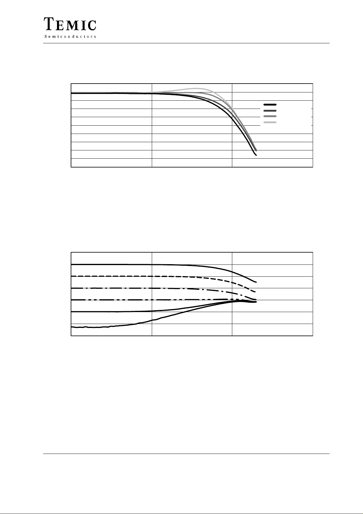
AC Characteristics
20
18
16
14
12
10
Gain ( dB )
8
6
4
2
0
1 10 100 1000
95 10748
Figure 4. Gain vs. frequency (various peaking), V12 = 12 V (contrast), V15 = V19 = V24 = 4 V (brightness)
U2203B
C = 0 pF
C = 10 pF
C = 27 pF
C = 47 pF
Frequency ( MHz )
10
0
–10
–20
–30
Relative gain ( dB )
–40
–50
–60
1 10 100 1000
Frequency ( MHz )95 10747
Figure 5. Relative gain vs. frequency (no peaking), V12 = variable (contrast), V15 = V19 = V24 = 4 V (brightness),
0 dBrel = 17.7 dB, C = 0 pF
TELEFUNKEN Semiconductors
Rev . A2, 27-Jan-97
5 (7)
Page 6
U2203B
10
0
–10
–20
–30
Releative gain ( dB )
–40
–50
–60
1 10 100 1000
Frequency ( MHz )95 10746
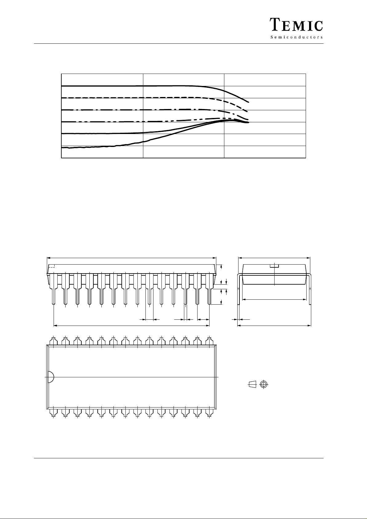
Figure 6. Rel. gain vs. frequency (optimized peaking), V12 = variable (contrast), V15 = V19 = V24 = 4 V (brightness),
0 dBrel = 17.7 dB, C = 27 pF
Package Information
Package DIP28
Dimensions in mm
28 15
37.40
36.90
1.54
33.02
0.58
0.48
2.54
4.0
3.8
3.3
0.8
0.5
0.35
0.25
technical drawings
according to DIN
specifications
15.29
15.19
13.9
13.7
16.1
15.3
13023
114
6 (7)
TELEFUNKEN Semiconductors
Rev . A2, 27-Jan-97
Page 7

U2203B
Ozone Depleting Substances Policy Statement
It is the policy of TEMIC TELEFUNKEN microelectronic GmbH to
1. Meet all present and future national and international statutory requirements.
2. Regularly and continuously improve the performance of our products, processes, distribution and operating systems
with respect to their impact on the health and safety of our employees and the public, as well as their impact on
the environment.
It is particular concern to control or eliminate releases of those substances into the atmosphere which are known as
ozone depleting substances (ODSs).
The Montreal Protocol ( 1987) and its London Amendments (1990) intend to severely restrict the use of ODSs and
forbid their use within the next ten years. Various national and international initiatives are pressing for an earlier ban
on these substances.
TEMIC TELEFUNKEN microelectronic GmbH semiconductor division has been able to use its policy of
continuous improvements to eliminate the use of ODSs listed in the following documents.
1. Annex A, B and list of transitional substances of the Montreal Protocol and the London Amendments respectively
2. Class I and II ozone depleting substances in the Clean Air Act Amendments of 1990 by the Environmental
Protection Agency (EPA) in the USA
3. Council Decision 88/540/EEC and 91/690/EEC Annex A, B and C (transitional substances) respectively.
TEMIC can certify that our semiconductors are not manufactured with ozone depleting substances and do not contain
such substances.
We reserve the right to make changes to improve technical design and may do so without further notice.
Parameters can vary in different applications. All operating parameters must be validated for each customer
application by the customer. Should the buyer use TEMIC products for any unintended or unauthorized
application, the buyer shall indemnify TEMIC against all claims, costs, damages, and expenses, arising out of,
directly or indirectly, any claim of personal damage, injury or death associated with such unintended or
unauthorized use.
TEMIC TELEFUNKEN microelectronic GmbH, P.O.B. 3535, D-74025 Heilbronn, Germany
Telephone: 49 (0)7131 67 2831, Fax number: 49 (0)7131 67 2423
TELEFUNKEN Semiconductors
Rev . A2, 27-Jan-97
7 (7)
 Loading...