

Simple Controller for Fast Charge Systems
Description
The bipolar IC U2407B is a fast charge battery controller
for drained NiCd/ NiMH batteries. Apart from phase
control, it is identical with U2405B, but has four LED
outputs. The IC enables the designer to create an efficient
and economic charge system. The U2407B incorporates
an intelligent multiple-gradient battery-voltage monitoring combined with temperature and failure mode
detection. With automatic top-off charging, the
integrated circuit ensures that the charge device stops
regular charging before the critical stage of overcharging
is achieved. It incorporates an additional algorithm for
reactivating fully drained batteries especially after long
time storage. It has four LED driver outputs for different
indications of the charge status.
U2407B
Features
D
Multiple gradient monitoring
D
Temperature window (T
D
Exact currentless measurement
D
Four LED status outputs
D
Linear power control
D
Preferred for externally regulated current sources
D
Preformation algorithm for drained batteries
D
Programmable top-off charge function
6.5 V/10 mA
16
14
1
Switch output
Power - on control
Power supply
= 8 to 26 V
V
S
V
min/Tmax
13
Ref
)
Applications
D
D
D
Package: DIP16/ SO16
12
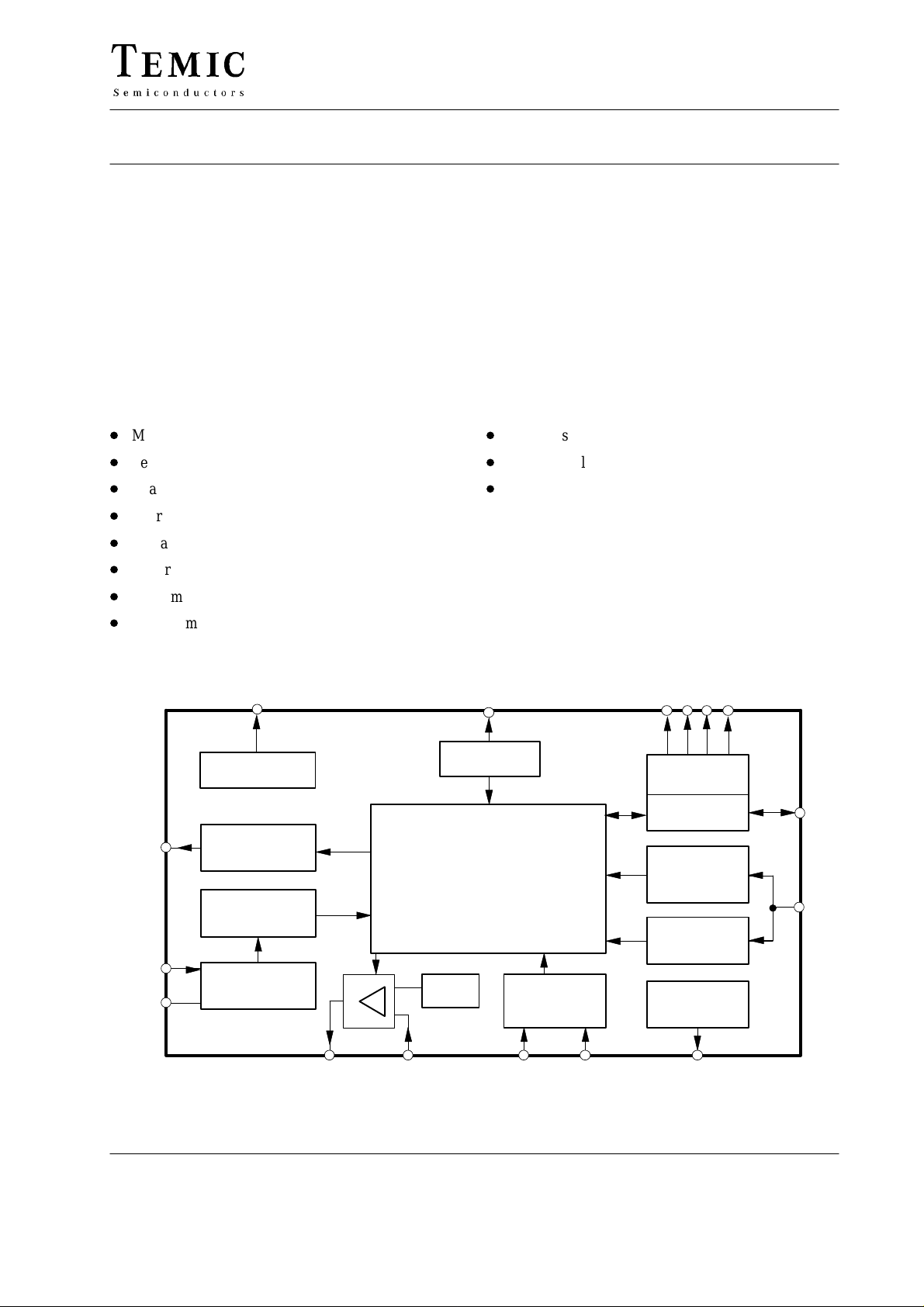
Oscillator
Control unit
Gradient
2
d
V/dt2 and –dV
160 mV
Ref
Primary switch mode
AC/ DC wall plug adapter
Ultra fast charger (10 minutes)
2
15
Status control
Scan path
Battery
detection
V
Ref
V
Batt
0.1 to 4 V
Temp. control
max
Sensor
T
Charge break
output
3
= 5 V
monitor
10
11
9
95 10648
TELEFUNKEN Semiconductors
Rev . A4, 05-Mar-97
4
5
Figure 1. Block diagram
67
8
1 (16)
U2407B
Input Voltage
8 V to 24 V
Mounted
heatsink
BYW52
Battery
10 mF
on
0.2
10
W
R
T
2
BC237
R
1 k
R
10 k
R
10 k
1
B1
W
B2
W
B3
W
R
1 k
W
BD649
T
1
I
ch
7
C
10
D
1
R
sh
W
2.2 k
10 k
R
R
4
W
100 k
6
W
R
8
W
1 mF
C
R
2.2 k
R
C
1 mF
C
1 mF
5
W
LED1
LED2
LED3
LED4
OP
V
7
Sensor
4
Batt
OP
O
I
V
S
10
2
3
15
4
U2407B
9
7
5
14
220 mF
C
1
GND
1
C
2
0.22 mF
V
Ref
13
R
T3
1.5 k
R
100 k
W
R
270 k
T2
W
O
W
95 10677
T
max
6
Output
16
Osc
12
C
O
8
t
S
p
TM
11
10 nF
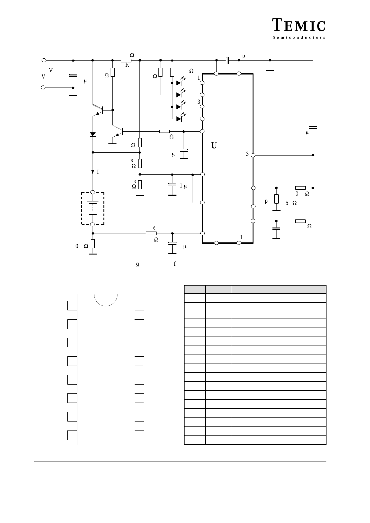
Pin Description
Package: DIP16/ SO16
GND
LED2
LED3
OP
OP
T
Sensor
t
p
O
max
1
2
3
4
5
I
6
7
8
Figure 2. Scheme for DC linear regulation
Pin Symbol Function
1 GND Ground
Output
16
15
LED4
2 LED2 Display output “top-off/ trickle
3 LED3 Display output “Fast charge”
4 OP
14
V
S
5 OPIOperational amplifier input
6 T
13
V
Ref
7 Sensor Temperature sensor
8 t
12
Osc
9 V
10 LED1 Display output “failure mode”
11 S
12 Osc Oscillator
13 V
14 V
15 LED4 Display output “top-off charge”
16 Output Trigger output
95 10618
11
10
9
S
TM
LED1
V
Batt
charge”
Operational amplifier output
O
Maximum temperature
max
Charge break output
p
Battery voltage
Batt
Test mode switch (status control)
TM.
Reference output voltage
Ref
Supply voltage
S
2 (16)
TELEFUNKEN Semiconductors
Rev . A3, 05-Mar-97
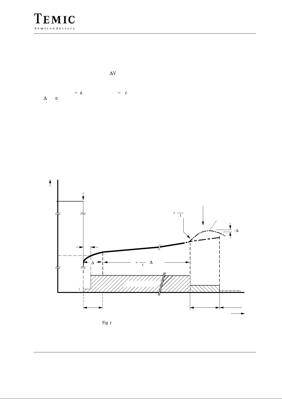
General Description
The integrated circuit, U2407B, is designed for charging
Nickel-Cadmium (NiCd) and Nickel-Metal-Hydride
(NiMH) batteries. Fast charging results in voltage lobes
when fully charged (figure 3). It supplies two
identifications (i.e., + d
charge operation at the proper time.
As compared to the existing charge concepts where the
charge is terminated * after voltage lobes * according
to – DV and temperature gradient identification, the
U2407B takes into consideration the additional changes
in positive charge curves, according to the second
derivative of the voltage with respect to time (d
The charge identification is the sure method of switching
off the fast charge before overcharging the battery. This
helps to give the battery a long life by hindering any
marked increase in cell pressure and temperature.
Even in critical charge applications, such as a reduced
charge current or with NiMH batteries where weaker
2
V/dt2, and – DV) to end the
2
V/dt2).
U2407B
charge characteristics are present multiple gradient
control results in very efficient switch-off.
An additional temperature control input increases not
only the performances of the charge switching
characteristics but also prevents the general charging of
a battery whose temperature is outside the specified
window.
A specific preformation algorithm is implemented for
reactivating fully drained batteries especially in the case
of batteries that have been stored for a long time.
A constant charge current is necessary for continued
charge-voltage characteristic. This constant current is
generated from an external power supply and can be regulated with the help of an internal op-amp regulator
(figure 2). An external current source can also be controlled by the switch output Pin 16 (see figure 12).
For further information please refer to the applications.
Battery
voltage
5 V
1.6 V
95 10616
Battery insertion
preformation
I (R
B1)
t1 = 5 min
–DV
)
Fast charge rate I
Figure 3. Charge function diagram, f
Fast charge stop
d
)
dt
2
d
V
,–DV
2
dt
O
= 800 Hz
osc
2
V
2
Top-off charge stop
without
charge control
Top-off
charge rate
1/4 I
O
t2 = 20 min
–DV
Trickle
charge rate
1/256 I
O
t
TELEFUNKEN Semiconductors
Rev . A4, 05-Mar-97
3 (16)
U2407B
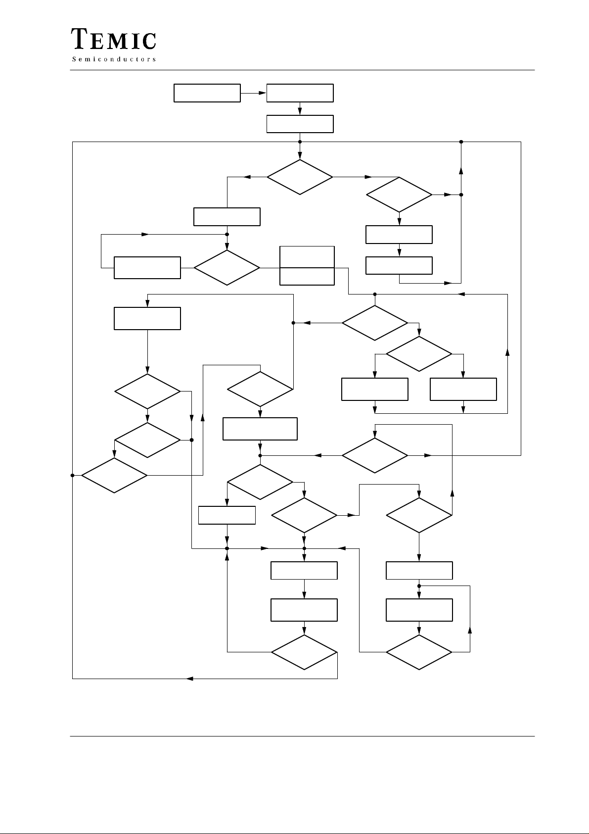
Flow Chart Explanation, f
= 800 Hz
osc
(Figures 2, 3 and 4)
Battery pack insertion disables the voltage lock at battery
detection input Pin 9. All functions in the integrated
circuit are reset. For further description, DIP-pinning is
taken into consideration.
Battery Insertion and –DV
Monitoring
After battery insertion fast charge Io begins when the
input voltage V
5 minutes the d
–DV monitoring is activated. In case the detected V
voltage is less then 1.6 V the special preformation
procedure will be activated. The reference level with
respect to the cell voltage can be adjusted by the resistor
(see figure 2).
R
B3
Preformation Procedure
Before fast charge of fully drained or long-time stored
batteries begins, a reactivation of it is necessary. The
preformation current is dependent on pull-up resistor
. The fast charge starts only after the V
R
B1
than 1.6 V. During the first 10 minutes the green LED2 is
blinking. If after 10 minutes, V
reached the reference level, the indication changes to red
blinking LED1. The charge will continue with
preformation rate I (R
reference level, the fast charge rate current, I
switched-on and the green LED2 is blinking.
–DV Cut-Off (Monitoring)
When the signal at Pin 9 of the DA converter is 12 mV
below the actual value, the comparator identifies it as a
voltage drop of –DV. The validity of –DV cut-off is
considered only if the actual value is below 12 mV for
three consecutive cycles of measurement.
d2V/dt2-Gradient
If there is no charge stop within the first 5 minutes after
battery insertion, then d
In this actual charge stage, all stop-charge criteria are
active.
is higher than 1.6 V. For the first
Batt
2
V/dt2-gradient recognition is suppressed,
is higher
Batt
voltage has not
Batt
). In case V
B1
2
V/dt2 monitoring will be active.
increases to 1.6 V
Batt
o
Batt
, is
Top-Off Charge Stage
By charge disconnection through the +d2V/dt
device switches automatically to a defined protective
top-off charge with a pulse rate of 1/4 I
= 5.12 s, period, T = 20.48 s).
t
p
The top-off charge time is specified for a time of
20 minutes @ 800 Hz.
During top-off mode the LED4 is in ON mode.
2
mode, the
(pulse time,
O
Trickle Charge Stage
When top-off charge is terminated, the device switches
automatically to trickle charge with 1/256 I
(tp = 5.12 s,
O
period = 1310.72 s). The trickle continues until the
battery pack is removed.
During trickle mode the LED2 output is in on mode,
LED4 is in OFF-mode.
Basic Description
Power Supply, Figure 2
The charge controller allows the direct power supply of
8 to 26 V at Pin 14. Internal regulation limits higher input
voltages. Series resistance, R
, to a maximum value of 25 mA. Series resistance
rent, I
S
is recommended to suppress the noise signal, even below
26 V limitation. It is calculated as follows.
1min
R
1max
v
25 mA
V
min
–8V
I
tot
–26 V
V
max
w
R
where
I
= IS + I
tot
V
max, Vmin
I
= Current consumption (IC) without load
S
I
= Current through resistance, R
RB1
+ I
RB1
1
= Rectified voltage
I1 = Trigger current at Pin 1
, regulates the supply cur-
1
B1
When close to the battery’s capacity limit, the battery
2
voltage curve will typically rise. As soon as the +d
V/dt
stop-charging criteria are met, the device will stop the fast
charge activities.
4 (16)
2
TELEFUNKEN Semiconductors
Rev . A3, 05-Mar-97
U2407B
*) 70 mV > V
LED1 blinking
Fast charge
begins
Batt
> 5V
Start
no
Reset
Temp. range
ok ?
Power on reset
LED1,2,3,4 off
yes
Batt. inserted
yes
*)
Preformation
current I
RB1
LED3 blinking
yes
no
V
Temp. range
Charge stop
LED1 blinking
> 1.6 V
Batt
yes
no
ok ?
yes
no
tch > 10 min
V
4 V
Batt
yes
–dV
switch off
no
no yes
Batt. inserted
*)
no
yes
Charge time
t
–dV and d2V/dt
monitoring activated
no
LED1 blinking
> 5 min ?
1
Batt temp
range?
yes yes
no
2
yes
–dV
disconnect
LED2 on
Trickle charge
1/256 I
O
Batt. inserted
*)
yes
no
LED1 blinking
Batt. inserted
*)
no
no
2
d2V/dt
disconnect ?
LED2 on
LED4 on
Top off charge
1/4 I
O
t2 > 20 min
LED3 off
no
no
95 10671
TELEFUNKEN Semiconductors
Rev . A4, 05-Mar-97
Figure 4. Flow chart
5 (16)

U2407B
Battery Voltage Measurement
The battery voltage measurement at Pin 9 (ADCconverter) has a range of 0 V to 4 V, which means a
battery pack containing two cells can be connected
without a voltage divider.
If the AD converter is overloaded (V
switch-off occurs. The fast charge cycle is terminated by
automatically changing to trickle charge.
Precaution should be taken that under specified charge
current conditions, the final voltage at the input of the
converter, Pin 9, should not exceed the threshold voltage
level of the reset comparator, which is 5 V. When the
battery is removed, the input (Pin 9) is terminated across
the pulled-up resistance, R
to the value of 5 V-reset-
B1,
threshold. In this way, the start of a new charge sequence
is guaranteed when a battery is reinserted.
If the battery voltage exceeds the converter range of 4 V,
adjusting it by the external voltage divider resistance, R
and RB3 is recommended.
w 4 V) a safety
Batt
B2
Value of the resistance, R
= 1 kW, RB2 = 10 kW, as follows:
R
B1
V
RB3+
R
B2
10max
V
Bmax–V10max
The minimum supply voltage, V
is calculated by assuming
B3
, is calculated for
smin
reset function after removing the inserted battery
according to:
ǒ
R
B3
B1
smin
0.03mA@R
+
V
)
Ǔ
R
)
5VǒR
B2
R
B3
)
RB2)
B1
R
B3
where:
V
V
V
= Max voltage at Pin 9
9max
= Min supply voltage at the IC (Pin 14)
Smin
= Max battery voltage
Bmax
The voltage conditions mentioned above are measured
during charge current break (switch-off condition).
Ǔ
14
V
S
V
DAC
- dV Recognition
R
B1
–
+
V
=
Ref
12 mV
=
V
DAC
DAC control
comparator
9
–
+
Reset
7 V
V
Ref
4.3 V
=
comparator
–
+
Reset
V
= 0.1 V
Ref
V
B
95 10623
Table 1. valid when V
V
6
10max
I
ch
R
Battery
R
sh
Figure 5. Input configuration for the battery voltage measurement
= 3.5 V
B2
R
B3
V
Batt
Cell No. 1 2 3 4 5 6 7 8 9 10 11 12
V
(V) 8 8 8 9 11 13 15 17 19 21 23 25
Smin
RB3 (k
W)
– – 51 16 10 7.5 5.6 4.7 3.9 3.3 3 2.7
6 (16)
TELEFUNKEN Semiconductors
Rev . A3, 05-Mar-97

U2407B
Analog-Digital-Converter (ADC),
Test Sequence
A special analog-digital-converter consists of a five-bit
coarse and a five-bit fine converter . It operates by a linear
count method which can digitalize a battery voltage of
4 V at Pin 9 in 6.5 mV steps of sensitivity.
In a duty cycle, T, of 20.48 s, the converter executes the
measurement from a standard oscillator frequency of f
= 800 Hz. The voltage measurement is during the charge
break time of 2.56 s (see figure 6), i.e., no-load voltage
(or currentless phase). Therefore it has optimum measurement accuracy because all interferences are cut-off
during this period (e.g., terminal resistances or dynamic
load current fluctuations).
After a delay of 1.28 s the actual measurement phase of
1.28 s follows. During this idle interval of cut-off
conditions, battery voltage is stabilized and hence
measurement is possible.
An output pulse of 10 ms appears at Pin 8 during charge
break after a delay of 40 ms. The output signal can be used
in a variety of way, e.g., synchronising the test control
(reference measurement).
osc
Plausibility for Charge Break
There are two criteria considered for charge break
plausibility:
– DV Cut-Off
When the signal at Pin 9 of the DA converter is 12 mV
below the actual value, the comparator identifies it as a
voltage drop of – DV. The validity of – DV cutt-off is
considered only if the actual value is below 12 mV for
three consective cycles of measurement.
d2V/dt2 Cut-Off
A four bit forward/ backward counter is used to register
the slope change (d
clocked by each tracking phase of the fine AD-counter.
Beginning from its initial value, the counter counts the
first eight cycles in forward direction and the next eight
cycles in reverse direction. At the end of 16 cycles, the
actual value is compared with the initial value. If there is
a difference of more than two LSB-bit (13.5 mV) from the
actual counter value, then there is an identification of
slope change which leads to normal charge cut-off. A
second counter in the same configuration is operating in
parallel with eight clock cycles delay, to reduce the total
cut-off delay, from 16 test cycles to eight test cycles.
2
V/dt2, V
– slope). This counter is
Batt
Status
charge
break
output
ADC
conversion
time
(internal)
Charge break
2.56 s
10 ms
40 ms
1.28 s 1.28 s
94 8693
Charge
t
T= 20.48 s
t
t
TELEFUNKEN Semiconductors
Rev . A4, 05-Mar-97
Figure 6. Operating sequence of voltage measurements
7 (16)

U2407B
Temperature Control, Figure 7
When the battery temperature is not inside the specified
temperature windows, the overal temperature control will
not allow the charge process. Sensor short circuit or
interruption also leads to switch-off (faulty mode).
A permanent switch-off follows after a measurement
period of 20.48 s, if the temperature exceeds a specified
level, which is denoted by a status of LED1. A charge
sequence will start only when the specified window
temperature range is attained.
The temperature window is specified between two
voltage transitions. The upper voltage transition is
specified by the internal reference voltage of 4 V, and the
lower voltage transition is represented by the external
voltage divider resistances R
and RT3.
T2
V
V
Ref
Ref
13
NTC sensors are normally used to control the temperature
of the battery pack. If the resistance values of NTC are
known for maximum and minimum conditions of
allowable temperature, then other resistance values, R
and RT3 are calculated as follows:
R
T2
suppose R
= 100 kW, then
T2
R
+
R
T1
RT3+
R
NTCmax
NTCmin
V
–4V
Ref
4V
R
T2
R
T1
T1
If NTC sensors are not used, then select the circuit
configuration according to figure 10.
,
R
T2
T
max
7
R
T1
R
T3
7 V
Sensor
8
NTC
sensor
Figure 7. Temperature window
7 V
Current Regulation
The charge concept requires a constant charge current
supply outside of the circuit. This is achieved by an
external switchable current source or by an internal error
amplifier regulation of an externally situated power
stage.
+
–
V
= 4 V
Ref
+
–
High
temperature
Low
temperature
95 10622
Charge Current Regulation, Figure 2
According to figure 2 the operational amplifier (OpAmp)
regulates the charge current, I
age value. The OpAmp detects the voltage drop across the
shunt resistor (R
) at input Pin 5 as an actual value. The
sh
actual value will then be compared with an internal reference value of 160 mV.
(= 160 mV/ Rsh), aver-
ch
8 (16)
TELEFUNKEN Semiconductors
Rev . A3, 05-Mar-97

U2407B
Status Control
Different status control modes can be designed by four LED outputs. Status control regards the running charge cycle
before it has been started and also after it has been terminated.
LED1 LED2 LED3 LED4 Status
OFF OFF OFF OFF No battery (V
OFF OFF Blinking OFF Fast charge
OFF ON OFF ON Top-off charge
OFF ON OFF OFF Trickle charge
Blinking OFF OFF OFF Failure mode
Failure mode: Temperature out of window, also before battery insertion or power-on.
Battery break, short circuit, V
Batt
< 0.1 V
To achieve custom specific display modes, several combinations between LED outputs 1 to 4 are recommended.
(see applications)
The blink frequency of LED outputs can be calculated as follows:
Batt
> 5 V)
(LED)
1024
Oscillator frequency, f
+
f
Example 1:
Display mode similar to U2402B and U2405B:
LED1
LED2
LED3
10
2
3
red
1 k
green
1 k
Figure 8.
V
W
V
W
95 10672
Example 2:
LED1
LED2
LED3
10
2
3
red
V
S
green
1 k
1 k
osc
LED1 (red) LED2 (green)
S
(LED1) (LED2/ LED3)
Status
OFF OFF No battery
(V
> 5 V)
Batt
S
OFF Blinking Fast charge
OFF ON Top-off, trickle charge
Blinking OFF All failure mode
Batt
Status
> 5 V)
LED1 (red) LED2 (green)
V
S
W
V
S
W
(LED1/ LED3) (LED2)
OFF OFF No battery
(V
ON OFF Fast charge
OFF ON Top-off, trickle charge
Blinking OFF All failure mode
Figure 9.
TELEFUNKEN Semiconductors
Rev . A4, 05-Mar-97
95 10673
9 (16)

U2407B
Top-off Charge Rate Reduction
The current amplitude during top-off charge can be
reduced as shown in figure 10. During top-off mode, both
the LED4 output (Pin 15) and transistor T are on. The
actual current amplitude is influenced with the help of
resistor R
input OP
depends on the reciprocal value of R
LED4
, which is detected by the operational amplifier
x
(Pin 5). The decrease of the current flow
1
95 10674
T
.
x
V
Ref
15
R
x
5
OP
I
Figure 10.
Battery
R
sh
Oscillator
Time sequences regarding measured values and
evaluation are determined by the system oscillator. All
the technical data given in the description are with the
standard frequency 800 Hz.
It is possibe to alter the frequency range in a certain
limitation. Figure 11 shows the frequency versus
resistance curves with different capacitance values.
Oscillation Frequency Adjustment
Recommendations:
0.5C charge 0.5 500 Hz = 250 Hz
1C charge 500 Hz
2C charge 2 500 Hz = 1000 Hz
3C charge 3 500 Hz = 1500 Hz
10000
1000
W
O
R ( k )
95 11408
CO=2.2nF
CO=10nF
100
10
0.1 1
fO ( kHz )
Figure 11. Frequency versus resistance for different capacitance values
CO=4.7nF
10
10 (16)
TELEFUNKEN Semiconductors
Rev . A3, 05-Mar-97

Absolute Maximum Ratings
Reference point Pin 2 (GND), unless otherwise specified
Parameters Symbol Value Unit
Supply voltage Pin 14 V
Voltage limitation IS = 10 mA
Current limitation Pin 14
t < 100 ms
Voltages at different pins Pins 16, 2, 3, 10 and 15
Pins 11 up to 13, 4 up to 9
Currents at different pins Pin 1
Pins 3 up to 14 and 16 up to 18
Power dissipation T
= 60°C P
amb
Ambient temperature range T
Junction temperature T
Storage temperature range T
Thermal Resistance
Parameters Symbol Maximum Unit
Junction ambient R
S
26 V
31
I
S
25
100
V 26
I 25
10
tot
amb
j
stg
thJA
650 mW
– 10 to +85 °C
125 °C
– 40 to +125 °C
100 K/W
U2407B
mA
V
7
mA
Electrical Characteristics
VS = 12 V, T
Power supply Pin 14
Voltage range V
Power-on threshold ON
Current consumption without load I
Reference Pin 13
Reference voltage I
Reference current – I
Temperature coefficient TC – 0.7 mV/K
Operational amplifier OP
Output voltage range I5 = 0 Pin 4 V
Output current range V5 = 3.25 V Pin 4 ±I
Output pause current Pin 4 –I
Non-inverting input voltage Pin 5 V
Non-inverting input current Pin 5 ±I
Comparator or temperature control
Input current Pins 6 and 7 ±I
Input voltage range Pins 6 and 7 V
Threshold voltage Pin 7 V
Charge break output Pin 8
Output voltage High, I8 = 4 mA
Output current V8 = 1 V I
= 25°C, reference point Pin 1 (GND), unless otherwise specified
amb
Parameters Test Conditions / Pins Symbol Min. T yp. Max. Unit
8 26 V
3.0
4.7
3.8
5.7
3.9 9.1 mA
6.19
6.14
6.5
6.5
6.71
6.77
10 mA
0.15 5.8 V
80
100
m
m
0 5 V
0.5
0.5
m
m
0 5 V
3.85 4.15 V
8.4
100
mV
10 mA
V
V
V
V
V
OFF
= 5 mA
Ref
I
= 10 mA
Ref
Low, I
= 0 mA
8
V
V
pause
V
S
S
S
Ref
Ref
4
4
5
5
6, 7
6, 7
7
8
8
A
A
A
A
TELEFUNKEN Semiconductors
Rev . A4, 05-Mar-97
11 (16)

U2407B
11
m
Battery detection Pin 9
Analog-digital converter Conversion range
Full scale level
Input current
0.1 V v V
v 4.5 V
Batt
Input voltage for reset V
Input current for reset
V
Batt
y 5 V
Battery detection Maximum voltage
Hysteresis Maximum voltage V
Mode select Pin 11
Treshold voltage Testmode V
Input current I
Input current Normal mode Pin 11 open
Sync. oscillator Pin 12
Frequency R = 150 kW, C = 10 nF f
Threshold voltage High level
Low level
Input current I
– I
D
V
V
V
I
V
Batt
Batt
Batt
Batt
Batt
hys
11
11
osc
T(H)
T(L)
12
0
4.0 V
3.85
0.5
4.8 5.0 5.3 V
8 35
80 120 mV
15 mV
4.7 V
20
0
800 Hz
4.3"3%
2.2"3%
– 0.5 0.5
UnitMax.Typ.Min.SymbolTest Conditions / PinsParameters
m
A
m
A
m
A
V
m
A
Applications
Input voltage
8 V to 26 V
current source
Battery
10
R
C
10
10 mF
Controlled
I
ch
C
100 mF
10
15
1
V
S
14
2
3
GND
1
13
C
2
0.22 mF
V
Ref
OP
4
O
W
1
R
B1
1 k
W
off
on
2.2 k
R
2
W
R
5
2.2 k
W
LED1
LED2
LED3
LED4
U2407B
R
B2
10 k
R
B3
16 k
Output
W
R
W
C
4.7 mF
T1
100 k
7
Sensor
R
14
510 k
16
V
Batt
9
W
7
W
8
11
12
OP
T
max
Osc
10 nF
I
R
O
270 k
W
C
O
5
6
12 (16)
t
p
Figure 12. Minimum charge system with external current source
S
TM
95 10675
TELEFUNKEN Semiconductors
Rev . A3, 05-Mar-97

U2407B
1
C
S
V
1
R
1
R
Master Slave
S
V
1
C
F
m
10
C
10
typ 12 V
Input voltage
W
10
W
10
m
R
R
R
R
R
R
m
F
100
5
4
7
7
4
5
F
100
W
2.2k
W
1M
W
1k
on
mounted
W
1k
W
1M
W
2.2k
1
14
green
red
1
T
heatsink
1
T
red
green
14
1
GND
S
V
BD649
BD649
S
V
GND
2
2
16
LED2
LED2
16
Ref
V
OUTPUT
LED1
10
3
D
1N4148
1
D
1
D
3
D
1N4148
10
LED1
OUTPUT
Ref
V
13
Ref
V
LED3
3
9
R
+
1/2LM393
BYW52
BYW52
8
1/2LM393
9
R
3
LED3
Ref
V
13
2
C
W
1k
3
C
–
2
T
2
T
3
C
W
1k
2
C
m
0.22 F
U2407B
F
m
4.7
Ref
V
BC237
I
I
BC237
4
Ref
V
F
m
4.7
U2407B
m
0.22 F
W
T2
R
15
6
LED4
O
OP
4
8
R
c
c
8
R
4
O
W
W
47k
47k
9
R
F
C
m
1
10
R
W
A2
10k
R
W
A2
R
10k
R
F
C
m
1
9
OP
LED4
15
6
T2
R
W
T3
100k
2.7k
R
max
T
Batt
V
Sensor
7
F
7
m
1
C
W
10k
W
A3
10k
R
W
A3
R
10k
7
F
C
m
1
7
Batt
V
Sensor
max
T
W
T3
W
R
2.7k
100k
W
O
R
270k
O
C
10nF
12622
12
OSC
TM
11
S
p
8
t
I
OP
4
5
F
C
m
1
W
... 1M
W
11
R
100k
Top off /
trickle
reduction
W
6
R
10k
R
W
6
R
10k
11
R
sh
W
0.2
W
... 1M
W
3
T
BC212
13
R
2
D
trickle
Top off /
reduction
12
R
W
100k
1N4148
W
100k
Ref
V
Ref
V
100k
F
4
m
1
C
5
I
OP
p
8
t
TM
11
S
OSC
12
W
270k
O
C
10nF
O
R
TELEFUNKEN Semiconductors
Rev . A4, 05-Mar-97
Figure 13. Dual–slot charger
13 (16)

U2407B
Package Information
Package DIP16 (CEI)
Dimensions in mm
1.60
0.64
0.58
0.38
1.65
1.14
20.57
18.92
0.81
2.79
2.29
3.81
3.05
3.81
3.05
0.76
0.13
0.89
0.38
technical drawings
according to DIN
specifications
7.87
7.37
6.60
6.10
0.38
0.20
9.40
7.62
13014
Package DIP16
Dimensions in mm
Alternative
20.0 max
4.8 max
3.3
0.5 min
17.78
0.58
0.48
2.54
technical drawings
according to DIN
specifications
1.64
1.44
16 9
18
7.82
7.42
6.4 max
0.39 max
9.75
8.15
13015
14 (16)
TELEFUNKEN Semiconductors
Rev . A3, 05-Mar-97

Package Information
Package SO16
Dimensions in mm
0.4
1.27
16 9
10.0
9.85
8.89
1.4
0.25
0.10
5.2
4.8
3.7
3.8
6.15
5.85
technical drawings
according to DIN
specifications
U2407B
0.2
13036
18
TELEFUNKEN Semiconductors
Rev . A4, 05-Mar-97
15 (16)

U2407B
Ozone Depleting Substances Policy Statement
It is the policy of TEMIC TELEFUNKEN microelectronic GmbH to
1. Meet all present and future national and international statutory requirements.
2. Regularly and continuously improve the performance of our products, processes, distribution and operating systems
with respect to their impact on the health and safety of our employees and the public, as well as their impact on
the environment.
It is particular concern to control or eliminate releases of those substances into the atmosphere which are known as
ozone depleting substances (ODSs).
The Montreal Protocol ( 1987) and its London Amendments (1990) intend to severely restrict the use of ODSs and
forbid their use within the next ten years. Various national and international initiatives are pressing for an earlier ban
on these substances.
TEMIC TELEFUNKEN microelectronic GmbH semiconductor division has been able to use its policy of
continuous improvements to eliminate the use of ODSs listed in the following documents.
1. Annex A, B and list of transitional substances of the Montreal Protocol and the London Amendments respectively
2. Class I and II ozone depleting substances in the Clean Air Act Amendments of 1990 by the Environmental
Protection Agency (EPA) in the USA
3. Council Decision 88/540/EEC and 91/690/EEC Annex A, B and C (transitional substances) respectively.
TEMIC can certify that our semiconductors are not manufactured with ozone depleting substances and do not contain
such substances.
We reserve the right to make changes to improve technical design and may do so without further notice.
Parameters can vary in different applications. All operating parameters must be validated for each customer
application by the customer. Should the buyer use TEMIC products for any unintended or unauthorized
application, the buyer shall indemnify TEMIC against all claims, costs, damages, and expenses, arising out of,
directly or indirectly, any claim of personal damage, injury or death associated with such unintended or
unauthorized use.
16 (16)
TEMIC TELEFUNKEN microelectronic GmbH, P.O.B. 3535, D-74025 Heilbronn, Germany
Telephone: 49 (0)7131 67 2831, Fax number: 49 (0)7131 67 2423
TELEFUNKEN Semiconductors
Rev . A3, 05-Mar-97
 Loading...