Charge Timer
Description
The U2403B is a monolithic, integrated-bipolar circuit
which can be used in applications for time-controlled,
constant-current charge. Selection of charge current
versus timing is carried out by using the external circuit
at Pins 2, 3 and 4. For high current requirement, an
external transistor is recommended in series with the
battery. To protect the IC against high power loss
U2403B
(typically > 140°C), the oscillator is shut down when the
reference voltage is switched off (0 V). The latter also
takes place when there is a saturation caused by collector
voltage at Pin 1. When the overtemperature has
disappeared and the collector voltage at Pin 1 has
exceeded the supply voltage (V
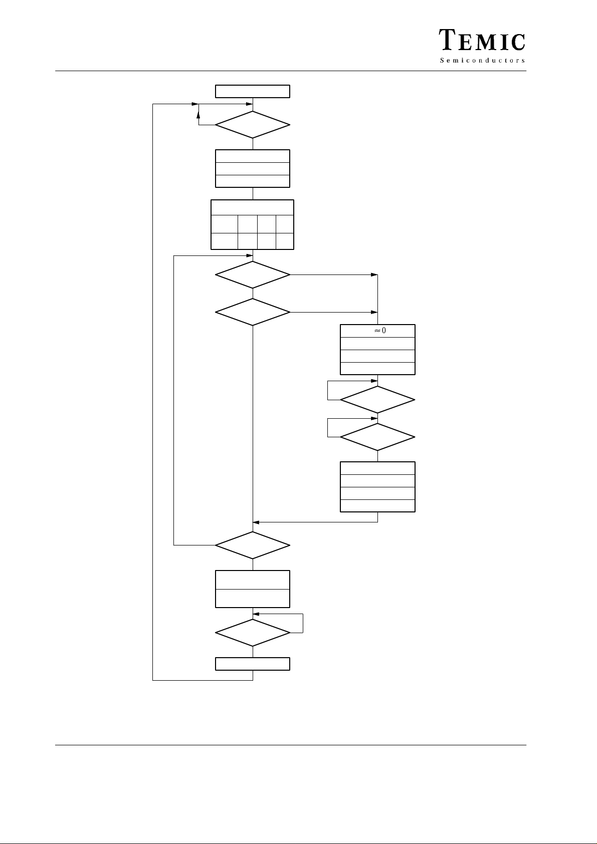
operation continues (see flow chart in figure 3).
> VS), charge time
1
Features
D
Easy-to-run autonomous dual rate charger
D
Constant charge current
D
3 h – 24 h charge time programmable
D
Low cost dc regulator
D
Overtemperature protection
D
Charge-mode indication
D
Operation starts at the moment of battery insertion
D
Fast charge time-test mode
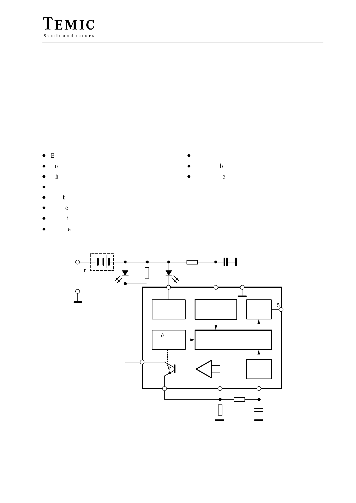
Block Diagram
LED
Power
supply
AC/DC
Battery
inserted
2
Charge
R
5
LED
8
Charge mode
indicator
Applications
D
Cordless telephones
D
Low-cost battery-charge timer
D
Entertainment
Package: DIP8, SO8
R
1
LED
1
Ready
V
Power supply
V
= 3.5 to 12 V
S
C
1
GND
S
6
7
Test
mode
94 8629
S
5
TM
TELEFUNKEN Semiconductors
Rev . A2, 14–Nov–96
í
max
140°C
1
V
1
Shunt
Figure 1. Block diagram with external circuit
í
2
Timer and control logic
= 1.5 V/ 0.1 V/ 0 V
V
Ref
V
Ref
+
–
Sense
R
3
R
4
RC
oscillator
43
Osc
C
4
1 (12)

U2403B
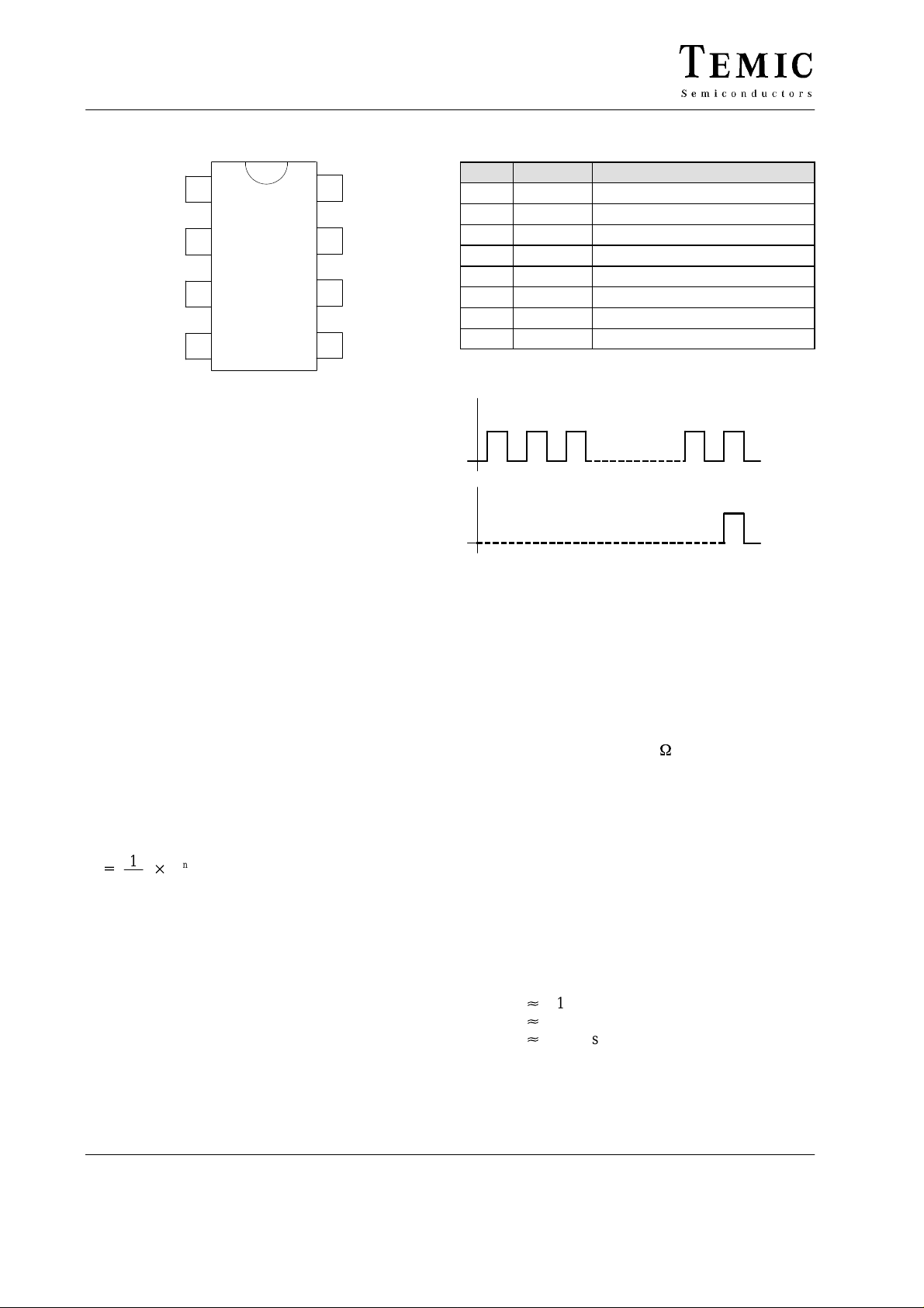
Pin Description
1
V
1
2
V
2
Sense
Osc
3
4
Pin 1, Collector Voltage V
94 8685
1
8
LED
7
GND
6
V
S
S
5
TM
Pin 1 is an open collector output. When V1 ≤ 3 V, the
charge cycle is switched off until it is above the supply
voltage, as shown in figure 6.
Pin 2, Shunt Emitter
The constant current source is supplied by the internal
operational amplifier. The voltage across R
is deter-
3
mined via the internal reference source.
Ich = V3/R3(V3 = V
sense
)
Pin 3, Amplifier Sense Input (Inverted)
Pin Symbol Function
1 V
2 V
3 V
Collector terminal
1
Shunt emitter terminal
2
Amplifier sense input
3
4 Osc Oscillator input
5 S
6 V
TM
Test mode switch
Supply voltage
S
7 GND Reference point, GND
8 LED Charge mode indicator
2 3 256
1
Pin 4
Pin 5
Figure 2. Quick test timer 1/3
Oscillator
Test – Mode
Pulse
94 8839
The voltage-regulated current source has a closed loop at
Pin 2, Pin 3, and resistor R
Pin 4, Oscillator Input R4, C
.
3
4
Selection of current charge versus timing is carried out by
using the external circuit at Pins 2, 3, and 4. Typical
values are given in charge characteristics (see table next
page).
Pin 5, Test-Mode Switch for Charging Time
The charging time, t
1
+
t
ch
osc
2
f
where:
f
= oscillator frequency (see figure 2)
osc
n = frequency divider
= 26, if S
= 17, if S
= 8, if S
The first eight divider stages can be tested directly.
256 input tact signals at Pin 4 create one tact signal at
Pin 5.
is given by the following equation.
ch,
n
open
TM
= GND
TM
= V
TM
S
Example
Assume a charge time of 6 h.
Select the values of R
For example: R
and C4 from the tables next page.
4
= 470 k
4
= 680 pF
C
4
W
There is a frequency of approximately 3100 Hz at Pin 4.
It is possible to test the charge time of 6 h by running
through the charge cycle for a very short time. By
connecting Pin 5 with GND, the test time is 42 s. By
connecting Pin 5 with Pin 1 (V
to about 82.4 ms. R
is connected in parallel to the LED
5
), the test time is reduced
1
and provides a protective bypass function for the LED
(see figure 1).
Pin 6, Supply Voltage, V
S
VS [ 3.1 V power-on reset release (turn-on)
[ 2.9 V under-voltage reset
V
S
[ 13 V supply voltage limitation
V
S
Pin 7, Ground
2
2 (12)
TELEFUNKEN Semiconductors
Rev . A1, 20-Mar-96

U2403B
Pin 8, Charge Mode Indicator
An open-collector output supplies constant current to
after the active charge phase has been terminated.
LED
1
controls the function temperature for the final stage
í
max
range. This is when the temperature is above 140°C and
the charge function is therefore switched off.
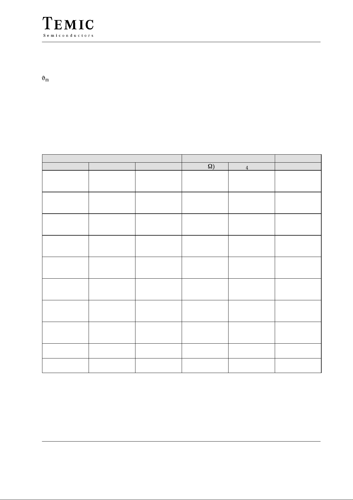
Charge Characteristics
Charge Time
Test time/ Test-Mode Switch S
Open V
3 h 41.2 ms 21 s 510
4 h 54.9 ms 28 s 620
5 h 68.6 ms 35 s 510
6 h 82.4 ms 42 s 620
7 h 96.1 ms 49 s 560
8 h 109.8 ms 56 s 620
9 h 123.6 ms 1 min 3 s 750
10 h 137.3 ms 1 min 10 s 620
12 h 164.8 ms 1 min 24 s 390
16 h 219.7 ms 1 min 56 s 470
S
TM
GND R4 (K
Trickle Charge
The trickle charge starts after the charge has been terminated. In this case, the internal reference voltage is
reduced from 1.5 V to approximately 0.1 V. This means
the charge current is decreased by the factor:
K = 1.5 V/ 0.1 V = 15.
Trickle current = I
It is possible to reduce the trickle charge with resistor R
as shown in figures 6 and 7.
Oscillator Components Frequency
W)
430
300
430
300
390
300
470
360
430
220
470
200
510
240
270
130
150
200
/ 15 + I6 (supply current) + I
ch
C4 (pF) f
270
330
470
330
470
680
470
680
1000
470
680
1000
680
1000
2200
680
1000
2200
680
1000
2200
820
2200
4700
2200
4700
2200
4700
osc
6213
4660
3728
3105
2663
2330
2071
1864
1553
1165
8
(Hz)
6,
TELEFUNKEN Semiconductors
Rev . A2, 14–Nov–96
3 (12)

U2403B
start
no
Battery
inserted
Turn on VS > 3.5 V
V
= 1.5 V
3
LED2 “ON”
Timer start
Test
Open
mode
Divider
2262172
Tj > T
V1 < 3.0 V
GND
max
no
no
V
S
8
yes
yes
V3[
0 V
Interrupt charging
LED2 “OFF”
Interrupt
no
Tj < T
max
no
End of
timing
LED2 “OFF”
LED
1
Trickle charge mode
= 100 mV
V
3
Battery
removed
Undervoltage reset
Figure 3. Flow chart
yes
“ON”
yes
yes
no
V1 > V
S
yes
V3 = 0 V
Continuous charging
LED2 “ON”
Continuous timing
no
95 9624
4 (12)
TELEFUNKEN Semiconductors
Rev . A1, 20-Mar-96

Absolute Maximum Ratings
Reference point Pin 7 (GND), unless otherwise specified.
Parameters Symbol Value Unit
Supply current Pin 6
t ≤ 100 ms
Currents Pin 1
Pin 2
Pin 3
Pin 4
Pin 5
Pin 8
Voltages Pins 1, 3, 5, 6 and 8
Pin 2
Pin 4
Junction temperature T
Ambient temperature T
Storage temperature range T
I
i
I
–I
I
I
I
I
V
V
V
amb
S
1
4
5
8
stg
U2403B
20
s
100
300
2
3
310
1
15
–75 to +120
8
13.5
2
4
j
1.6
1.5
150 °C
10 to 85 °C
–50 to +150 °C
mA
mA
mA
mA
m
A
mA
m
A
mA
V
Thermal Resistance
Parameters Symbol Value Unit
Junction ambient
DIP8
SO8 on PC-board
SO8 on ceramic
SO8 on ceramic with thermal compound
R
thJA
120
220
140
80
K/W
TELEFUNKEN Semiconductors
Rev . A2, 14–Nov–96
5 (12)

U2403B
Electrical Characteristics
VS = 6 V, T
= 25_C, reference point Pin 7 (GND), unless otherwise specified.
amb
Parameters Test Conditions / Pins Symbol Min. Typ. Max. Unit
Supply voltage limitation Pin 6
= 4 mA
I
S
= 20 mA
I
S
Supply current VS = 6 V I
Voltage monitoring Pin 6
Turn-on threshold V
Turn-off threshold V
Charge-mode indicator (LED) Pin 8
LED current I
LED saturation voltage I8 = 3.7 mA V
Leakage current I
Collector terminal, Figure 5 Pin 1
Open collector current I
Saturation threshold VS = 6 V V
V
Shunt emitter current R3 = 5.6
W
Pin 2 I
Operational sense amplifier, Figure 1 Pin 3
Input current V3 = 0 V I
Input voltage V
Ref
V
Ref
V
Ref
= 1.5 V
= 100 mV
= 0 V
Oscillator Pin 4
Leakage current V4 = 0 to 0.85 V I
Threshold voltage Upper V
Oscillator frequency R4 = 160 kW, C4 = 2.2 nF
= 680 kW, C4 = 4.7 nF
R
4
Test mode switch (STM) Pin 5
Input current V5 = 6 V
= 0 V
V
5
Output voltage High
Low
V
TOFF
TOFF
V
f
V
V
S
S
TON
8
8
lkg
CO
TON
2
3
3
lkg
T(u)
osc
I
5
0(H)
0(L)
12.5
12.6
13.5
13.7
1.4 2.2 mA
2.8 3.5
2.5 3.2
3.0 6.0 mA
960 mV
–0.35 1.1
15 55
V
2.55
–1V
S
3.0
V
3.35
–0.4V
V
S
S
250 285 mA
–0.6 0.08
1.42
40
–0.4
1.5
70
1.58
100
40
–0.5 0.1
875 985 mV
2700
305
40
–75
1.7
0.5
3050
345
120
–20
2.5
1.0
V
V
m
A
m
A
V
m
A
V
mV
mV
m
A
Hz
mA
V
6 (12)
TELEFUNKEN Semiconductors
Rev . A1, 20-Mar-96

U2403B
Internal Temperature Switch
The internal temperature monitoring is active if the chip
temperature rises above 140°C. Above this temperature
the voltage at Pin 3 goes to zero. Similarly, the charge
current, I
I
= V3 / R
ch
where Ich = 1 to 2 mA (IC supply current)
The oscillator is connected to GND via Pin 3 (V
holds the present time status. When the chip temperature
decreases below the transition value, all functions are
released and the charge time is continued. The process is
reversible. If there is a higher power dissipation in the
circuit (T
permanently activated (ON). The total cycle time is
prolonged according to the interrupt-time duration, see
figure 4.
, reduces according to the equation:
ch
3
) which
3
> 140°C), the temperature monitoring remains
j
T
j
140°C
130°C
Automatic Control Protection
To reduce the design costs, it is possible to select the transformer which requires minimum power supply.
The output stage of the control is selected so that
it is switched off before saturation is achieved
= 3.0 V). In this case, the voltage at Pin 3 is kept
(V
CEsat
at a value of zero. The charge current is also zero and the
transformer is now an open circuit impedance. The
system becomes active again if V
The advantage of the system is that if sags of short
duration appear on the mains voltage or if the transformers used are too small, the charge duration is
increased, but the charge capacity remains the same (see
figure 5).
T
j
≥ VS.
1
95 9640
I
1
V
3.0 V
0 V
I
1
S
Charge current
Charge current
Timing
Timing
Charge mode
Figure 4. Charge duration – overtemperature
–V
1
Charge mode
Counting timer
Counting timer
t
95 9633
t
TELEFUNKEN Semiconductors
Rev . A2, 14–Nov–96
Figure 5. Charge duration – V
1
7 (12)

U2403B
Ch
h
C
V
g
g
Trickle charge:
Standard Applications
Basic Example
NiCd battery 750 mAh
arging time: 3
Charge current:
240 mA, 1/3 C
Trickle char
e:
19 mA < 1/40 C
Minimum Supply Voltage
No of Cells DC Supply Minimum
1
2
3
4
5
Special Requirements of Different Charge
Times
R1 = 510 W, 1/8 W
= 47
F/ 16
1
R3 = 6.2 , 1/2 W
R4 = 300 k
C4 = 470 pF
R
= 8.2 , 1/2 W
5
6.8 V
8.3 V
9.8 V
11.3 V
12.8 V
Basic Equations
R1 = 0.5 V / I
IS = 1.8 mA
= V5/ (Ich – 20 mA)
R
5
Nominal Charge Current:
= V3/R3 where V3 = 1.48 V (typ.)
I
ch
T rickle Current:
= V3/R3 + I8 + I
I
ch
Typical values are:
= 100 mV, I8 = 4.5 mA
V
3
DC
supply
R
5
S
READY
LED
Charge
LED
1
2
I
ch
S
R
1
8
7
65
U2403B
123
I
S
C
1
95 9639
4
R4, C4 values for different charging times
2 h 4 h 6 h 7 h 12 h
R
300 k430 k470 k470 k390 k
4
C
330 pF 470 pF 680 pF 1 nF 2.2 nF
4
Special Requirements for Different Charge
Current
R3, R5 values for different charge current
240 mA 150 mA 100 mA 50 mA
R
3
R
5
8.2
15
22
68
R
4
R
Figure 6. Standard application
3
C
4
8 (12)
TELEFUNKEN Semiconductors
Rev . A1, 20-Mar-96

U2403B
ging
Charging time: 2 h
C1 100 F/ 16 V
Trickl
R
300 k
Booster and Trickle Charge Reduction
Basic Example
NiCd battery 1000 mAh
Char
time: 2 h
Charge current: 500 mA
e charge:
22 mA < 1/22 C
R1 = 510 W, 1/8 W
C
= 100 F/ 16 V
1
R3 = 3 / 1 W
=
4
C4 = 330 pF
R5 = 3.9 / 1 W
C
= 1 F
2
Supply Voltage
No of Cells DC Supply Minimum
1
2
3
4
5
VS = 6.5 V
8.0 V
9.5 V
11.0 V
12.5 V
Basic Equations
R1 = 0.5 V / I
R5 = V(LED2)/ (Ich – 20 mA)
Nominal Charge Current:
Ich = V3/ R
T rickle Current:
Ich = V3/R3 + I
Typical values:
= 100 mV
V
3
= 4.5 mA
I
LED1
= 1.8 mA
I
S
Trickle-Charge Reduction (I
= (V
I
6
DC
supply
S
3
V3 = 1.48 V, typically
+ IS – I
LED1
+ VD1)/R
Batt
I
6
R
READY
6
I
ch
6
BYW52
D
1
6
8
)
6
VD1 = 0.75 V
R
1
LED
I
1
S
7
C
1
S1
65
Special Requirements for Different Charge
Times
R4, C4 values for different charge times
2 h 4 h 6 h 7 h 12 h
R
300 k430 k470 k470 k390 k
4
C
330 pF 470 pF 680 pF 1 nF 2.2 nF
4
Special Requirements for Different Charge
Current
R3, R5 values for different charge currents
616 mA 493 mA 411 mA 296 mA
R
3
R
5
R6 = 560 , reduced trickle charge
3
3.9
4.7
6.8
C
2
R
2
10 k
BD 136
or
BC 636
R
5
Figure 7. Application for charge current > 250 mA
Charge
LED
LED
S1: use for test only
U2403B
123
R
2
3
To fulfill requirements of higher charge current an external booster transistor can be used (see figure 7). As the
temperature cannot be monitored in this case a heat sink
with a resonable size should be used for safe operation.
Test mode switch S
can be used for accelerated produc-
1
tion check.
R
4
4
C
4
95 9623
TELEFUNKEN Semiconductors
Rev . A2, 14–Nov–96
9 (12)

U2403B
Charge System at Higher Voltage of 30 V
Charge systems with higher voltages than V
realized with the additional expander circuitry, as shown
in figure 8. This circuit contains a simple temperature
monitoring function. When the temperature level is
Smax
can be
reached, the transistor, T
, is switched on. If T3 is
3
switched on and there is current flow into Pin 5, normal
charge is terminated.
+
DC-Supply
30 V
–
LED1
red
TLHR5400
mounted
on
heatsink
R
+
–
5
T
2
Battery
NTC
R
1
I
ch
BC212
BD135
R
96 11707
R
11
R
10
T
3
BC212
D
1
green
R
2
TLHG5400
R
8
LED2
D
2
T
1
8
7
65
U2403B
C
R
7
6
2
1
234
LED1 normal charge
LED2 trickle charge
R1 = 1 kW, R2 = 10 kW, R3 = f(IC), R4 = f(time), R5 =10 kW/0.5 W, R6= 1 kW,
= 10 kW, R8 = 47 kW, R10 =10 kW, R11 = f(temp.), D1 = 1N4148, D2 = BZX85C10,
R
7
C
= 100 mF/6 V, C2 = 10 nF, C4 = 330 pF
1
R
= f(temp.) depends on number of cells
11
Figure 8. U2403B for higher supply voltage up to 30 V with integrated temperature monitoring
No of Cells R
2
3
4
5
13 k
8.2 k
6.2 k
4.7 k
11
W
W
W
W
NTC Value
25°C
40°C
50°C
10 (12)
R
4
R
3
C
4
6.8 k
3.9 k
2.8 k
W
W
W
TELEFUNKEN Semiconductors
Rev . A1, 20-Mar-96

Package Information
Package DIP8
Dimensions in mm
9.8
9.5
1.64
1.44
4.8 max
0.5 min
0.58
0.48
85
14
2.54
7.62
3.3
technical drawings
according to DIN
specifications
U2403B
7.77
7.47
6.4 max
0.36 max
9.8
8.2
13021
Package SO8
Dimensions in mm
5.00
4.85
1.4
0.4
1.27
3.81
85
85
0.25
0.10
5.2
4.8
3.7
3.8
6.15
5.85
technical drawings
according to DIN
specifications
0.2
13034
TELEFUNKEN Semiconductors
Rev . A2, 14–Nov–96
11 (12)

U2403B
Ozone Depleting Substances Policy Statement
It is the policy of TEMIC TELEFUNKEN microelectronic GmbH to
1. Meet all present and future national and international statutory requirements.
2. Regularly and continuously improve the performance of our products, processes, distribution and operating systems
with respect to their impact on the health and safety of our employees and the public, as well as their impact on
the environment.
It is particular concern to control or eliminate releases of those substances into the atmosphere which are known as
ozone depleting substances (ODSs).
The Montreal Protocol ( 1987) and its London Amendments (1990) intend to severely restrict the use of ODSs and
forbid their use within the next ten years. Various national and international initiatives are pressing for an earlier ban
on these substances.
TEMIC TELEFUNKEN microelectronic GmbH semiconductor division has been able to use its policy of
continuous improvements to eliminate the use of ODSs listed in the following documents.
1. Annex A, B and list of transitional substances of the Montreal Protocol and the London Amendments respectively
2. Class I and II ozone depleting substances in the Clean Air Act Amendments of 1990 by the Environmental
Protection Agency (EPA) in the USA
3. Council Decision 88/540/EEC and 91/690/EEC Annex A, B and C (transitional substances) respectively.
TEMIC can certify that our semiconductors are not manufactured with ozone depleting substances and do not contain
such substances.
We reserve the right to make changes to improve technical design and may do so without further notice.
Parameters can vary in different applications. All operating parameters must be validated for each customer
application by the customer. Should the buyer use TEMIC products for any unintended or unauthorized
application, the buyer shall indemnify TEMIC against all claims, costs, damages, and expenses, arising out of,
directly or indirectly, any claim of personal damage, injury or death associated with such unintended or
unauthorized use.
12 (12)
TEMIC TELEFUNKEN microelectronic GmbH, P.O.B. 3535, D-74025 Heilbronn, Germany
Telephone: 49 (0)7131 67 2831, Fax number: 49 (0)7131 67 2423
TELEFUNKEN Semiconductors
Rev . A1, 20-Mar-96
 Loading...