

Page 1
QUAD OPERATIONAL AMPLIFIERS
.
LOW OFFSETVOLTAGE: 500µVmax.
.
LOW POWERCONSUMPTION
.
SHORT CIRCUIT PROTECTION
.
LOW DISTORTION, LOW NOISE
.
HIGHGAIN-BANDWIDTHPRODUCT
.
HIGHCHANNEL SEPARATION
.
ESD INTERNALPROTECTION
.
MACROMODEL INCLUDED IN THIS
SPECIFICATION
DESCRIPTION
The TS514is ahighperformancequadoperational
amplifier with frequencyand phase compensation
builtintothechip.Theinternalphasecompensation
allows stable operationas voltagefollowerin spite
of its high gain-bandwidthproducts.
The circuit presents very stable electrical characteristics over the entire supply voltage range, and
it particularlyintendedfor professionalandtelecom
applications(active filters, etc).
TS514,A
HIGH SPEED PRECISION
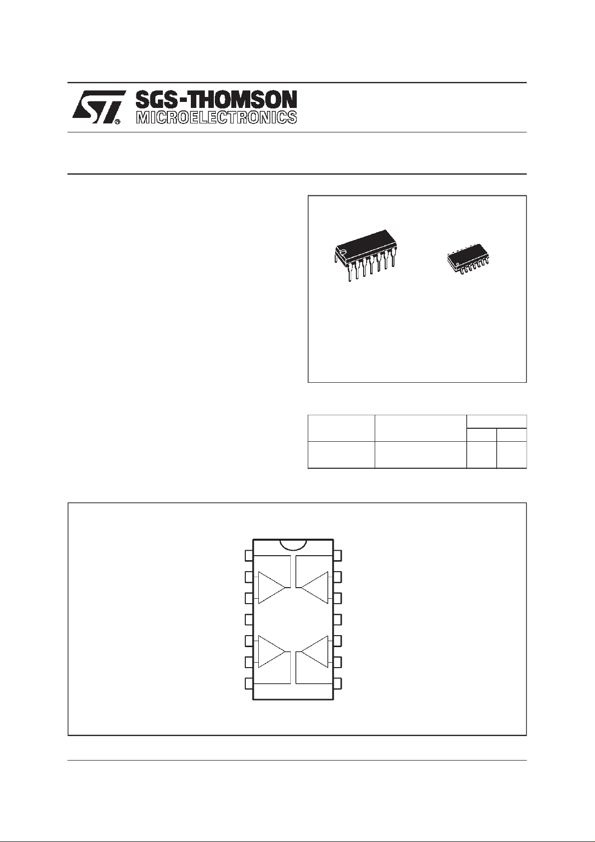
N
DIP14
(Plastic Package)
ORDER CODES
Part Number Temperature Range
TS514I -40
TS514AI -40
(Plastic Micropackage)
o
C, +125oC ••
o
C, +125oC ••
D
SO14
Package
ND
PINCONNECTIONS (top view)
Output 1
Inverting Input 1
Non-inverting Input 1
Non-inverting Input 2
Inverting Input 2
Output2
December 1997
1
2
-
+
3
+
CC
4
5
+
-
6
7
V
14
Output 4
Inverting Input 4
13
-
+
+
-
Non-inverting Input 4
12
-
V
11
CC
Non-inverting Input 3
10
Inverting Input 3
9
8
Output 3
1/7
Page 2
TS514,A
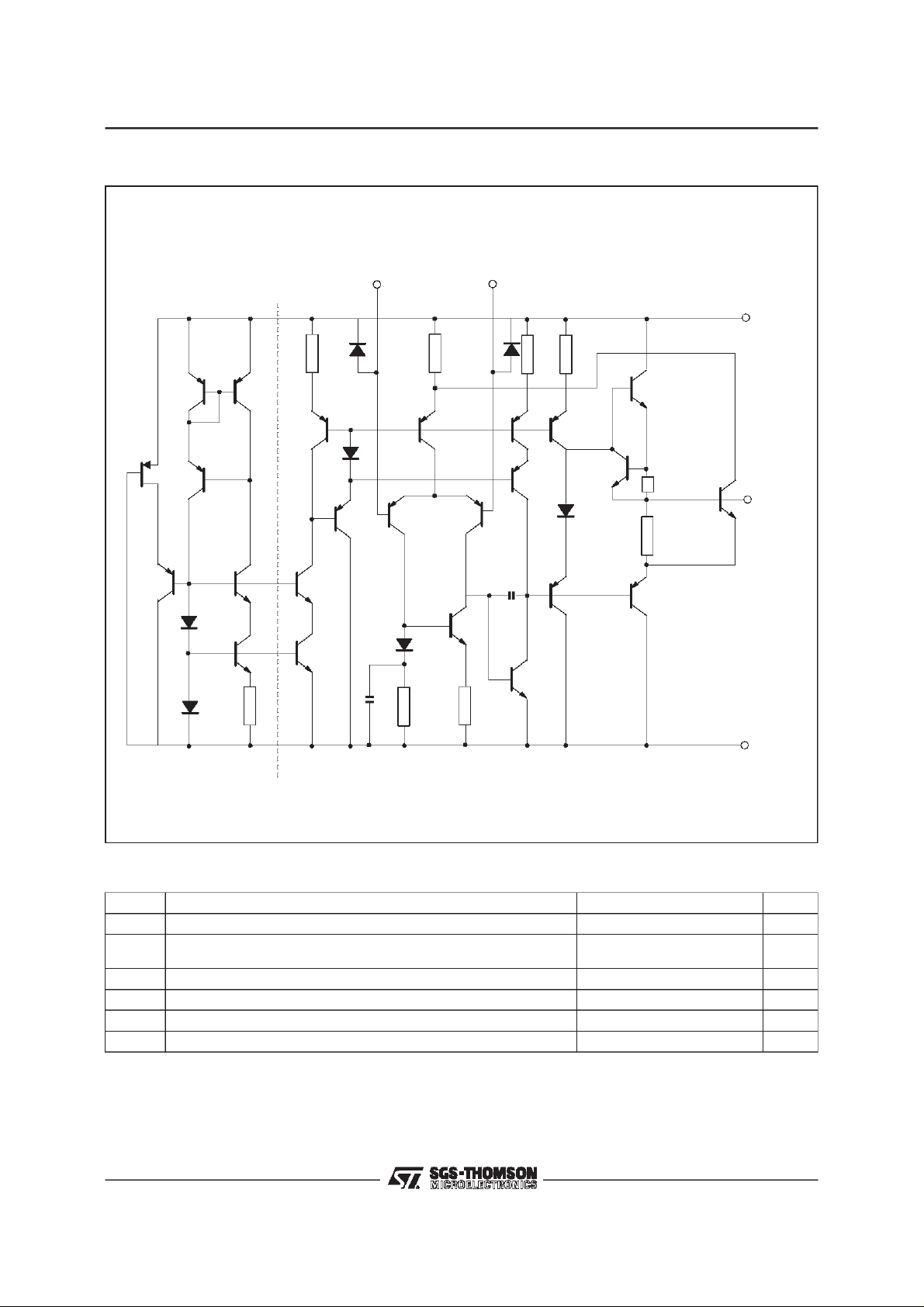
SCHEMATIC DIAGRAM (1/2 TS514)
Q17
R5
D3
D4
Q1
Q7
Q2
Q18
Q21
R8
Q3
Q19
Q22
R1
D6
Inverting
input
D1
Q8
D5
C2
Q10
R9
Non-inverting
R2
Q4
Q11
Q23
R10
input
D7
C1
Q9
Q20
Q5
R3
Q6
Q15
R4
D2
Q12
8
Q13
Q14
R6
Output
R7
Q16
4
ABSOLUTEMAXIMUM RATINGS
Symbol Parameter Value Unit
V
V
T
P
T
2/7
Supply Voltage ±18 V
CC
Input Voltage (positive)
V
i
Differential Input Voltage ± (VCC-1)
id
Operating Temperature Range -40 to +125
oper
Power Dissipation at T
tot
Storage Temperature -65to 150
stg
(negative)
=70oC 400 mW
amb
+V
CC
-VCC- 0.5
V
o
C
o
C
Page 3

TS514,A
ELECTRICALCHARACTERISTICS (VCC= ±15V,T
= 25oC, unless otherwise specified)
amb
Symbol Parameter Test Conditions Min. Typ. Max. Unit
I
R
V
DV
I
DI
I
A
Supply Current 1.4 2.4 mA
CC
Input Bias Current 50 150 nA
I
ib
T
min.<Top<Tmax
Input Resistance f = 1kHz 1 MΩ
i
Input Offset Voltage TS514
io
T
min.<Top<Tmax
Input Offset Voltage Drift T
io
Input Offset Current 5 20 nA
io
Input Offset Current Drift T
io
Output Short Circuit Current 23 mA
os
Large SignalVoltage Gain RL=2kΩ VCC= ±15V
vd
.<Top<T
min
.<Top<T
T
min
.<Top<T
min
. 300 nA
0.5 2.5
TS514A
. TS514
TS514A
.5µV/oC
max
.40nA
max
. 0.08 nA
max
90 100
= ±4V
V
CC
95
0.5
4
1.5
GBP Gain-bandwidth Product f = 100kHz 1.8 3 MHz
e
THD Total Harmonic Distortion A
±V
V
Equivalent Input Noise Voltage f = 1kHz
n
Output Voltage Swing RL=2kΩ VCC= ±15V
opp
Large SignalVoltage Swing RL= 10kΩ f = 10kHz 28 V
opp
=50Ω
R
s
=1kΩ
R
s
= 10kΩ
R
s
= 20dB RL=2kΩ
V
=2VPPf = 1kHz
V
O
V
CC
= ±4V
8
10
18
0.03 0.1 %
±13
±3
15
√Hz
SR Slew Rate Unity Gain, RL=2kΩ 0.8 1.5 V/µs
CMR Common Mode Rejection Ratio V
SVR Supply Voltage Rejection Ratio V
V
O1/VO2
Channel Separation f = 1kHz 100 120 dB
= 10V 90 dB
ic
= 1V f = 100Hz 90 dB
ic
mV
mV
°C
dB
nV
V
PP
3/7
Page 4

TS514,A
.
SINGLEOR SPLIT SUPPLYOPERATION
.
LOW POWERCONSUMPTION
.
SHORT CIRCUIT PROTECTION
Applies to : TS514i,AI
** Standard Linear Ics Macromodels, 1993.
** CONNECTIONS :
* 1 INVERTING INPUT
* 2 NON-INVERTING INPUT
* 3 OUTPUT
* 4 POSITIVEPOWER SUPPLY
* 5 NEGATIVEPOWER SUPPLY
.SUBCKT TS514 1 3 2 4 5 (analog)
**********************************************************
.MODEL MDTH D IS=1E-8 KF=6.647807E-16 CJO=10F
* INPUT STAGE
CIP 2 5 1.000000E-12
CIN 1 5 1.000000E-12
EIP 10 52 5 1
EIN 16 5 1 5 1
RIP 10 11 1.300000E+01
RIN 15 16 1.300000E+01
RIS 11 15 6.437882E+01
DIP 11 12 MDTH 400E-12
DIN 15 14 MDTH 400E-12
VOFP 12 13 DC 0
VOFN 13 14 DC 0
IPOL 13 52.000000E-05
CPS 11 15 9.75E-10
DINN 17 13 MDTH 400E-12
VIN 17 5 0.000000e+00
DINR 15 18 MDTH 400E-12
VIP 4 18 1.500000E+00
FCP 4 5 VOFP 1.525000E+01
FCN 5 4 VOFN 1.525000E+01
FIBP 2 5 VOFN 5.000000E-03
FIBN 5 1 VOFP 5.000000E-03
.
LOW DISTORTION,LOW NOISE
.
HIGHGAIN-BANDWIDTHPRODUCT
.
HIGHCHANNELSEPARATION
* AMPLIFYING STAGE
FIP 5 19 VOFP 1.125000E+03
FIN 5 19 VOFN 1.125000E+03
RG1 19 5 6.512062E+05
RG2 19 4 6.512062E+05
CC 19 29 1.500000E-08
HZTP 30 29 VOFP 8.944787E+02
HZTN 5 30 VOFN 8.944787E+02
DOPM 19 22 MDTH 400E-12
DONM 21 19 MDTH 400E-12
HOPM 22 28 VOUT 6.521739E+03
VIPM 28 4 1.500000E+02
HONM 21 27 VOUT 6.521739E+03
VINM 5 27 1.500000E+02
GCOMP 5 4 4 5 7.485029E-04
RPM1 5 80 1E+09
RPM2 4 80 1E+09
GAVPH 5 82 19 80 2.99E-03
RAVPHGH 82 4 668
RAVPHGB 82 5 668
RAVPHDH 82 83 1000
RAVPHDB 82 84 1000
CAVPHH 4 83 0.352E-09
CAVPHB 5 84 0.352E-09
EOUT 26 23 82 5 1
VOUT 23 5 0
ROUT 26 3 150
COUT 3 5 1.000000E-12
DOP 19 25 MDTH 400E-12
VOP 4 25 1.785252E+00
DON 24 19 MDTH 400E-12
VON 24 5 1.785252E+00
.ENDS
4/7
Page 5

ELECTRICALCHARACTERISTICS
= ±15V, T
V
CC
Symbol Conditions Value Unit
V
io
A
vd
I
CC
V
icm
V
OH
V
OL
I
sink
I
source
GBP R
SR R
_∅mR
=25oC (unless otherwise specified)
amb
0mV
RL=2kΩ 94 V/mV
No load, per operator 325 µA
-15 to 13.5 V
RL=2kΩ +13 V
RL=2kΩ -13 V
VO=0V 24 mA
VO=0V 24 mA
=2k
Ω,
L
L
L
CL= 100pF 3 MHz
=2k
Ω,
CL= 100pF 1.4 V/µs
=2k
Ω,
CL= 100pF 55 Degrees
TS514,A
5/7
Page 6

TS514,A
PACKAGE MECHANICALDATA
14 PINS - PLASTICDIP
Dim.
a1 0.51 0.020
B 1.39 1.65 0.055 0.065
b 0.5 0.020
b1 0.25 0.010
D 20 0.787
E 8.5 0.335
e 2.54 0.100
e3 15.24 0.600
F 7.1 0.280
i 5.1 0.201
L 3.3 0.130
Z 1.27 2.54 0.050 0.100
Min. Typ. Max. Min. Typ. Max.
Millimeters Inches
6/7
Page 7

PACKAGE MECHANICALDATA
14 PINS - PLASTICMICROPACKAGE(SO)
TS514,A
Dim.
Min. Typ. Max. Min. Typ. Max.
Millimeters Inches
A 1.75 0.069
a1 0.1 0.2 0.004 0.008
a2 1.6 0.063
b 0.35 0.46 0.014 0.018
b1 0.19 0.25 0.007 0.010
C 0.5 0.020
c1 45
o
(typ.)
D 8.55 8.75 0.336 0.334
E 5.8 6.2 0.228 0.244
e 1.27 0.050
e3 7.62 0.300
F 3.8 4.0 0.150 0.157
G 4.6 5.3 0.181 0.208
L 0.5 1.27 0.020 0.050
M 0.68 0.027
S8
Information furnishedis believed to be accurate and reliable. However, SGS-THOMSON Microelectronics assumes no responsibility
for the consequences of use of such information nor for any infringement ofpatents orother rights of third parties which may result
from its use. No license isgranted byimplication or otherwise underany patent or patentrights ofSGS-THOMSON Microelectronics.
Specifications mentioned in this publication are subject to change without notice. This publication supersedes and replaces all
information previouslysupplied. SGS-THOMSONMicroelectronics productsare not authorized for use as critical components in life
support devices or systems without express written approval of SGS-THOMSON Microelectronics.
o
(max.)
1997 SGS-THOMSON Microelectronics – Printed in Italy– All Rights Reserved
SGS-THOMSON Microelectronics GROUP OF COMPANIES
Australia -Brazil -Canada - China - France - Germany - Italy - Japan - Korea - Malaysia - Malta - Morocco
The Netherlands - Singapore - Spain - Sweden - Switzerland - Taiwan - Thailand - United Kingdom - U.S.A.
7/7
 Loading...