

Page 1
Features
TS4995
1.2W fully differential audio power amplifier
with selectable standby and 6db fixed gain
■ Differential inputs
■ 90dB PSRR @ 217Hz with grounded inputs
■ Operating from Vcc = 2.5V to 5.5V
■ 1.2W rail to rail output power @ Vcc=5V,
THD+N=1%, F=1kHz, with 8Ω load
■ 6dB integrated fixed gain
■ Ultra-low consumption in standby mode (10nA)
■ Selectable standby mode (active low or active
high)
■ Ultra-fast startup time: 10ms typ. at Vcc=3.3V
■ Available in 9-bump flip-chip (300mm bump
diameter)
■ Ultra-low pops&clicks
Description
The TS4995 is an audio power amplifier capable
of delivering 1.2W of continuous RMS output
power into an 8Ω load at 5V. Thanks to its
differential inputs, it exhibits outstanding noise
immunity.
An external standby mode control reduces the
supply current to less than 10nA. A STBY MODE
pin allows the standby pin to be active HIGH or
LOW. An internal thermal shutdown protection is
also provided, making the device capable of
sustaining short-circuits.
The TS4995 features an internal fixed gain at 6dB
which reduces the number of external
components on the application board.
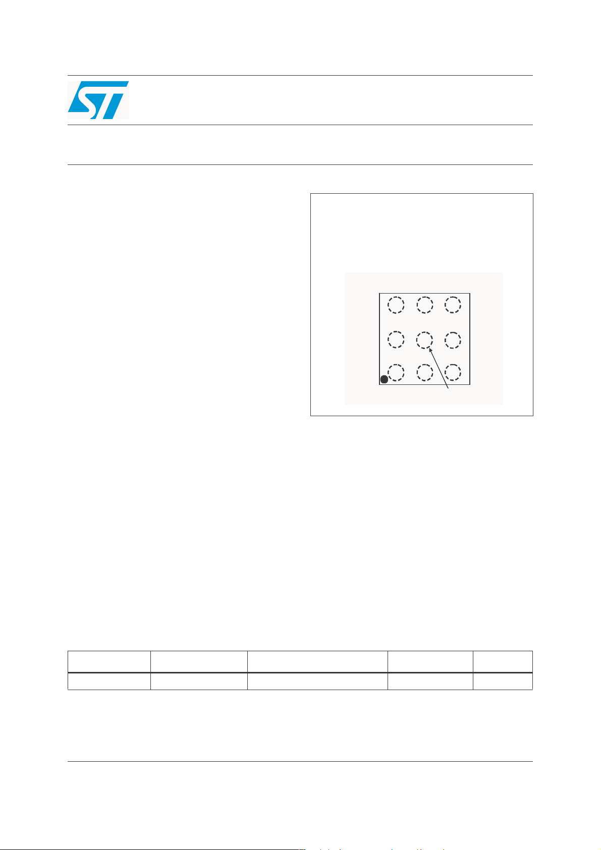
TS4995 - Flip-Chip9
Pin connections (top view)
Gnd
Gnd
V
V
Bypass Stdby
Bypass Stdby
V
V
765
765
O-
O-
8
8
IN+
IN+
1
1
9
9
2
2
V
V
CC
CC
V
V
O+
O+
4
4
V
V
3
3
IN-
IN-
Stdby Mode
Stdby Mode
The device is equipped with Common Mode
Feedback circuitry allowing outputs to be always
biased at Vcc/2 regardless of the input common
mode voltage.
The TS4995 has been designed for high quality
audio applications such as mobile phones and
requires few external components.
Applications
■ Mobile phones (cellular / cordless)
■ PDAs
■ Laptop / notebook computers
■ Portable audio devices
Device summary table
Part Number Temperature Range Package Packing Marking
TS4995EIJT -40°C to +85°C Lead free flip-chip9 Tape & Reel 95
June 2006 Rev. 1 1/24
www.st.com
24
Page 2

Contents TS4995
Contents
1 Absolute maximum ratings & operating conditions . . . . . . . . . . . . . . . 3
2 Typical application schematic . . . . . . . . . . . . . . . . . . . . . . . . . . . . . . . . . 4
3 Electrical characteristics . . . . . . . . . . . . . . . . . . . . . . . . . . . . . . . . . . . . . 5
4 Application information . . . . . . . . . . . . . . . . . . . . . . . . . . . . . . . . . . . . . 16
4.1 Differential configuration principle . . . . . . . . . . . . . . . . . . . . . . . . . . . . . . . 16
4.2 Common mode feedback loop limitations . . . . . . . . . . . . . . . . . . . . . . . . . 16
4.3 Low frequency response . . . . . . . . . . . . . . . . . . . . . . . . . . . . . . . . . . . . . . 16
4.4 Power dissipation and efficiency . . . . . . . . . . . . . . . . . . . . . . . . . . . . . . . . 17
4.5 Decoupling of the circuit . . . . . . . . . . . . . . . . . . . . . . . . . . . . . . . . . . . . . . 18
4.6 Wake-up Time: TWU . . . . . . . . . . . . . . . . . . . . . . . . . . . . . . . . . . . . . . . . 19
4.7 Shutdown time . . . . . . . . . . . . . . . . . . . . . . . . . . . . . . . . . . . . . . . . . . . . . 19
4.8 Pop performance . . . . . . . . . . . . . . . . . . . . . . . . . . . . . . . . . . . . . . . . . . . 19
4.9 Single-ended input configuration . . . . . . . . . . . . . . . . . . . . . . . . . . . . . . . 19
5 Package mechanical data . . . . . . . . . . . . . . . . . . . . . . . . . . . . . . . . . . . . 21
5.1 9-bump flip-chip package . . . . . . . . . . . . . . . . . . . . . . . . . . . . . . . . . . . . . 21
6 Revision history . . . . . . . . . . . . . . . . . . . . . . . . . . . . . . . . . . . . . . . . . . . 23
2/24
Page 3
TS4995 Absolute maximum ratings & operating conditions
1 Absolute maximum ratings & operating conditions
Table 1. Absolute maximum ratings (AMR)
Symbol Parameter Value Unit
V
CC
V
T
oper
T
stg
T
R
thja
P
diss
ESD
i
j
Supply voltage
Input voltage
Operating free air temperature range -40 to + 85 °C
Storage temperature -65 to +150 °C
Maximum junction temperature 150 °C
Thermal resistance junction to ambient
Power dissipation Internally limited W
Machine model 200 V
Human body model 1.5 kV
Latch-up Latch-up immunity 200 mA
- Lead temperature (soldering, 10sec) 260 °C
1. All voltage values are measured with respect to the ground pin.
2. The magnitude of input signal must never exceed VCC + 0.3V / GND - 0.3V.
3. Device is protected in case of over temperature by a thermal shutdown activated at 150°C.
Table 2. Operating conditions
Symbol Parameter Value Unit
V
Supply voltage 2.5 to 5.5 V
CC
Standby Mode Voltage Input:
V
SM
Standby Active LOW
Standby Active HIGH
Standby Voltage Input:
V
STB
Device ON (V
Device OFF (V
T
R
R
1. The minimum current consumption (I
temperature range.
Thermal Shutdown Temperature 150 °C
SD
Load Resistor ≥ 8 Ω
L
Thermal Resistance Junction to Ambient 100 °C/W
thja
(1)
(2)
(3)
=GND) or Device OFF (VSM=VCC)
SM
=GND) or Device ON (VSM=VCC)
SM
) is guaranteed when V
STANDBY
6V
GND to V
CC
200 °C/W
=GND
V
SM
V
SM=VCC
≤ V
STB
STB
≤ VCC
≤ 0.4
(1)
1.5 ≤ V
G
ND
= GND or VCC (i.e. supply rails) for the whole
STB
V
V
V
3/24
Page 4

Typical application schematic TS4995
2 Typical application schematic
Table 3. External components descriptions
Components Functional description
C
s
C
b
C
in
Supply Bypass capacitor which provides power supply filtering.
Bypass capacitor which provides half supply filtering.
Optional input capacitor making a high pass filter together with Rin. (fcl = 1 / (2 x Pi x Rin x Cin).
Figure 1. Typical application
TS4995
Op ti onal
Vin-
P1
P2
Vin+
Cin 1
330nF
Cin 2
330nF
3
1
8
Vin-
Vin+
BYPASS
BIAS
VCC
2
Cs1
1uF
TS4995 FlipChip
Vcc
Vo -
7
Vo+
+
5
8 Ohms
1uF
Cbyp as s1
VCC
3
STD BY
2
1
4
STDBY / Operation
STB Y
STDBY M ODE
9
3
4/24
GND
6
2
STDBY MODE
1
Page 5

TS4995 Electrical characteristics
3 Electrical characteristics
Table 4. VCC = +5V, GND = 0V, T
Symbol Parameter Test conditions Min. Typ. Max. Unit
I
Supply Current No input signal, no load 4 7 mA
CC
I
STANDBY
Voo
Standby Current
Differential Output Offset
Voltage
Input Common Mode Voltage - 0 4.5 V
V
IC
Po Output Power THD = 1% Max, F= 1kHz, RL = 8Ω 0.8 1.2 W
= 25°C (unless otherwise specified)
amb
No input signal, Vstdby = V
No input signal, Vstdby = V
= GND, RL = 8Ω
SM
= VCC, RL = 8Ω
SM
10 1000 nA
No input signal, RL = 8Ω 0.1 10 mV
THD + N
PSRR
CMRR
SNR Signal-to-Noise Ratio
GBP Gain Bandwidth Product R
Total Harmonic Distortion +
Noise
Power Supply Rejection Ratio
IG
with Inputs Grounded
Common Mode Rejection
Ratio
V
Output Voltage Noise
N
(1)
Po = 850mW rms, 20Hz ≤ F ≤ 20kHz, RL = 8Ω 0.5 %
F = 217Hz, R = 8Ω, Cin = 4.7µF, Cb =1µF
Vripple = 200mV
F = 217Hz, RL = 8Ω, C
Vic = 200mV
PP
PP
= 4.7µF, Cb =1µF
in
75
(2)
90 dB
60 dB
A Weighted Filter
= 8Ω, THD +N < 0.7%, 20Hz ≤ F ≤ 20kHz 100
R
L
= 8Ω 2MHz
L
20Hz ≤ F ≤ 20kHz, R
Unweighted
A weighted
Unweighted, Standby
A weighted, Standby
= 8Ω
L
11
7
3.5
1.5
Zin Input impedance - 15 20 25 kΩ
- Gain mismatch - 5.5 6 6.5 dB
T
1. Dynamic measurements - 20*log(rms(Vout)/rms (Vripple)). Vripple is the super-imposed sinus signal relative to Vcc.
2. Guaranteed by design and evaluation.
3. Transition time from standby mode to fully operational amplifier.
WU
Wake-Up Time
(3)
Cb =1µF15mS
µV
dB
RM
S
5/24
Page 6
Electrical characteristics TS4995
Table 5. VCC = +3.3V (all electrical values are guaranteed with correlation measurements at
2.6V and 5V), GND = 0V, T
Symbol Parameter Test conditions Min. Typ. Max. Unit
Supply Current No input signal, no load 3 7 mA
I
CC
I
STANDBY
Voo
THD + N
Standby Current
Differential Output Offset
Voltage
Input Common Mode Voltage - 0.4 2.3 V
V
IC
Po Output Power THD = 1% Max, F= 1kHz, RL = 8Ω 300 500 mW
Total Harmonic Distortion +
Noise
= 25°C (unless otherwise specified)
amb
No input signal, Vstdby = V
No input signal, Vstdby = V
= GND, RL = 8Ω
SM
= VCC, RL = 8Ω
SM
10 1000 nA
No input signal, RL = 8Ω 0.1 10 mV
Po = 300mW rms, 20Hz ≤ F ≤ 20kHz, RL = 8Ω 0.5 %
PSRR
CMRR
Power Supply Rejection Ratio
IG
with Inputs Grounded
Common Mode Rejection
Ratio
(1)
SNR Signal-to-Noise Ratio
GBP Gain Bandwidth Product R
V
Output Voltage Noise
N
F = 217Hz, R = 8Ω, Cin = 4.7µF, Cb =1µF
Vripple = 200mV
F = 217Hz, RL = 8Ω, C
Vic = 200mV
PP
PP
= 4.7µF, Cb =1µF
in
75
(2)
90 dB
60 dB
A Weighted Filter
RL = 8Ω, THD +N < 0.7%, 20Hz ≤ F ≤ 20kHz 100
= 8Ω 2MHz
L
20Hz ≤ F ≤ 20kHz, R
Unweighted
A weighted
Unweighted, Standby
A weighted, Standby
= 8Ω
L
11
7
3.5
1.5
Zin Input impedance - 15 20 25 kΩ
- Gain mismatch - 5.5 6 6.5 dB
T
1. Dynamic measurements - 20*log(rms(Vout)/rms (Vripple)). Vripple is the super-imposed sinus signal relative to Vcc.
2. Guaranteed by design and evaluation.
3. Transition time from standby mode to fully operational amplifier.
WU
Wake-Up Time
(3)
Cb =1µF10mS
µV
dB
RM
S
6/24
Page 7
TS4995 Electrical characteristics
Table 6. VCC = +2.6V, GND = 0V, T
Symbol Parameter Test conditions Min. Typ. Max. Unit
Supply Current No input signal, no load 3 7 mA
I
CC
I
STANDBY
Voo
THD + N
Standby Current
Differential Output Offset
Voltage
Input Common Mode Voltage - 0.6 1.5 V
V
IC
Po Output Power THD = 1% Max, F= 1kHz, RL = 8Ω 200 300 mW
Total Harmonic Distortion +
Noise
= 25°C (unless otherwise specified)
amb
No input signal, Vstdby = V
No input signal, Vstdby = V
= GND, RL = 8Ω
SM
= VCC, RL = 8Ω
SM
10 1000 nA
No input signal, RL = 8Ω 0.1 10 mV
Po = 225mW rms, 20Hz ≤ F ≤ 20kHz, RL = 8Ω 0.5 %
PSRR
CMRR
Power Supply Rejection Ratio
IG
with Inputs Grounded
Common Mode Rejection
Ratio
(1)
SNR Signal-to-Noise Ratio
GBP Gain Bandwidth Product R
V
Output Voltage Noise
N
F = 217Hz, R = 8Ω, Cin = 4.7µF, Cb =1µF
Vripple = 200mV
F = 217Hz, RL = 8Ω, C
Vic = 200mV
PP
PP
= 4.7µF, Cb =1µF
in
75
(2)
90 dB
60 dB
A Weighted Filter
RL = 8Ω, THD +N < 0.7%, 20Hz ≤ F ≤ 20kHz 100
= 8Ω 2MHz
L
20Hz ≤ F ≤ 20kHz, R
Unweighted
A weighted
Unweighted, Standby
A weighted, Standby
= 8Ω
L
11
7
3.5
1.5
Zin Input impedance - 15 20 25 kΩ
- Gain mismatch - 5.5 6 6.5 dB
T
1. Dynamic measurements - 20*log(rms(Vout)/rms (Vripple)). Vripple is the super-imposed sinus signal relative to Vcc.
2. Guaranteed by design and evaluation.
3. Transition time from standby mode to fully operational amplifier.
WU
Wake-Up Time
(3)
Cb =1µF10mS
µV
dB
RM
S
7/24
Page 8
Electrical characteristics TS4995
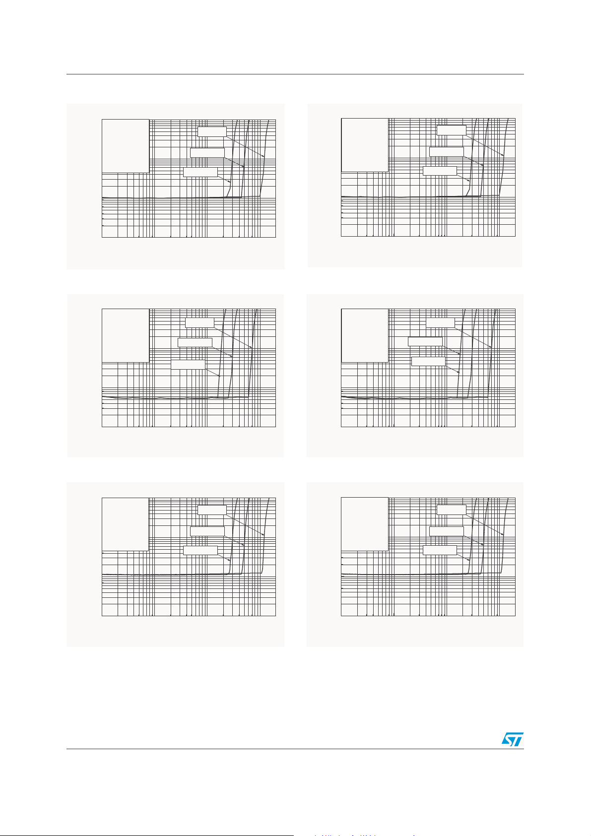
Figure 2. THD+N vs. output power Figure 3. THD+N vs. output power
10
RL = 8
Ω
G = 6dB
F = 20Hz
Cb = 1µF
BW < 125kHz
1
Tamb = 25°C
0.1
THD + N (%)
0.01
1E-3 0.01 0.1 1
Output power (W)
Vcc=5V
Vcc=3.3V
Vcc=2.6V
10
RL = 8
Ω
G = 6dB
F = 20Hz
Cb = 0
BW < 125kHz
1
Tamb = 25°C
0.1
THD + N (%)
0.01
1E-3 0.01 0.1 1
Output power (W)
Vcc=5V
Vcc=3.3V
Vcc=2.6V
Figure 4. THD+N vs. output power Figure 5. THD+N vs. output power
THD + N (%)
0.1
10
RL = 16
G = 6dB
F = 20Hz
Cb = 1µF
BW < 125kHz
1
Tamb = 25°C
Ω
Vcc=5V
Vcc=3.3V
Vcc=2.6V
10
THD + N (%)
0.1
RL = 16
G = 6dB
F = 20Hz
Cb = 0
BW < 125kHz
1
Tamb = 25°C
Ω
Vcc=5V
Vcc=3.3V
Vcc=2.6V
0.01
1E-3 0.01 0.1 1
Output power (W)
0.01
1E-3 0.01 0.1 1
Output power (W)
Figure 6. THD+N vs. output power Figure 7. THD+N vs. output power
10
RL = 8
Ω
G = 6dB
F = 1kHz
Cb = 1µF
BW < 125kHz
1
Tamb = 25°C
0.1
THD + N (%)
0.01
1E-3 0.01 0.1 1
Output power (W)
Vcc=5V
Vcc=3.3V
Vcc=2.6V
10
RL = 8
Ω
G = 6dB
F = 1kHz
Cb = 0
BW < 125kHz
1
Tamb = 25°C
0.1
THD + N (%)
0.01
1E-3 0.01 0.1 1
Output power (W)
Vcc=5V
Vcc=3.3V
Vcc=2.6V
8/24
Page 9

TS4995 Electrical characteristics
Figure 8. THD+N vs. output power Figure 9. THD+N vs. output power
10
RL = 16
Ω
G = 6dB
F = 1kHz
Cb = 1µF
1
BW < 125kHz
Tamb = 25°C
THD + N (%)
0.1
0.01
1E-3 0.01 0.1 1
Output power (W)
Vcc=5V
Vcc=3.3V
Vcc=2.6V
10
RL = 16
Ω
G = 6dB
F = 1kHz
Cb = 0
1
BW < 125kHz
Tamb = 25°C
0.1
THD + N (%)
0.01
1E-3 0.01 0.1 1
Output power (W)
Vcc=5V
Vcc=3.3V
Vcc=2.6V
Figure 10. THD+N vs. output power Figure 11. THD+N vs. output power
10
1
THD + N (%)
RL = 8
Ω
G = 6dB
F = 20kHz
Cb = 1µF
BW < 12 5kHz
Tamb = 25°C
Vcc=5V
Vcc=3.3V
Vcc=2.6V
10
1
THD + N (%)
RL = 8
Ω
G = 6dB
F = 20kHz
Cb = 0
BW < 12 5kHz
Tamb = 25°C
Vcc=5V
Vcc=3.3V
Vcc=2.6V
0.1
1E-3 0.01 0.1 1
Output po wer (W)
0.1
1E-3 0.01 0.1 1
Output po wer (W)
Figure 12. THD+N vs. output power Figure 13. THD+N vs. output power
10
RL = 16
Ω
G = 6dB
F = 20kHz
Cb = 1µF
1
BW < 125kHz
Tamb = 25°C
0.1
THD + N (%)
0.01
1E-3 0.01 0.1 1
Output power (W)
Vcc=5V
Vcc=3.3V
Vcc=2.6V
10
RL = 16
Ω
G = 6dB
F = 20kHz
Cb = 0
1
BW < 125kHz
Tamb = 25°C
0.1
THD + N (%)
0.01
1E-3 0.01 0.1 1
Output power (W)
Vcc=5V
Vcc=3.3V
Vcc=2.6V
9/24
Page 10

Electrical characteristics TS4995
Figure 14. THD+N vs. frequency Figure 15. THD+N vs. frequency
10
RL = 8
G = 6dB
Cb = 1µF
BW < 125kHz
Tamb = 25C
1
Ω
Vcc=2.6V, Po=225mW
10
RL = 8
G = 6dB
Cb = 0
BW < 125kHz
Tamb = 25C
1
Ω
Vcc=2.6 V, Po=225 mW
THD + N (%)
0.1
0.01
Vcc=5V, Po=850mW
THD + N (%)
Vcc=3.3V, Po=300mW
100 1000 10000
Frequency (Hz)
0.1
0.01
Vcc=5V, Po=850mW
Vcc=3.3V, Po=300mW
100 1000 10000
Frequency (Hz)
Figure 16. THD+N vs. frequency Figure 17. THD+N vs. frequency
THD + N (%)
0.1
0.01
10
RL = 16
G = 6dB
Cb = 1µF
BW < 125kHz
Tamb = 25C
1
Ω
Vcc=5V, Po=500mW
Vcc=2.6V, Po=125mW
Vcc=3.3V, Po=225mW
100 1000 10000
Frequency (Hz)
THD + N (%)
0.01
10
1
0.1
RL = 16
Ω
G = 6dB
Cb = 0
BW < 125kHz
Tamb = 25C
Vcc=5V, Po=500mW
Vcc=2.6V, Po=125mW
Vcc=3.3V, Po=225mW
100 1000 10000
Frequency (Hz)
Figure 18. Output power vs. power supply
voltage
10
RL = 16
Ω
G = 6dB
Cb = 1µF
BW < 125kHz
Tamb = 25C
1
Vcc=5V, Po=500mW
THD + N (%)
0.1
0.01
10/24
Vcc=2.6V, Po=125mW
Vcc=3.3V, Po=225mW
100 1000 10000
Frequency (Hz)
Figure 19. Output power vs. power supply
voltage
1.8
Cb = 1µF
1.6
F = 1kHz
BW < 12 5 kHz
1.4
Tamb = 25°C
1.2
1.0
0.8
0.6
0.4
0.2
Output power at 10% TH D + N (W)
0.0
2.53.03.54.04.55.0 5.5
8
Ω
Vcc (V)
16
Ω
32
Ω
Page 11

TS4995 Electrical characteristics
Figure 20. Output power vs. load resistance Figure 21. Power dissipation vs. output
power
THD+N = 1%
F = 1kHz
Cb = 1µF
BW < 125kHz
Tamb = 25°C
Vcc=3.3V
Vcc=2.6V
Output power (W)
1400
1200
1000
800
600
400
200
0
Vcc=5.5V
Vcc=5V
Vcc=4.5V
Vcc=4V
8 101214161820222426283032
Load Resistance (Ω)
Figure 22. Power dissipation vs. output
power
300
250
200
150
100
Power D issipat ion (mW)
50
0
0 100 200 300 400 500
RL=16
RL=8
Ω
Ω
Output Power (mW)
Vcc = 3.3V
F = 1kHz
THD+N < 1%
700
600
500
400
300
200
Power Dissipation (mW)
100
0
RL=16
0 200 400 600 800 1000 1200
RL=8
Ω
Ω
Output Power (mW)
Vcc = 5V
F = 1kHz
THD+N < 1%
Figure 23. Power dissipation vs. output
power
200
180
160
140
RL=8
120
100
80
60
40
Power Dissipation (mW)
20
0
0 50 100 150 200 250 300
RL=16
Ω
Output Power (mW)
Ω
Vcc = 2.6V
F = 1kHz
THD+N < 1%
Figure 24. PSSR vs. frequency Figure 25. PSSR vs. frequency
0
Vcc = 2.6V
-10
Vripple = 200mVpp
-20
RL ≥ 8
-30
G = 6dB, Cin = 4.7µF
Inputs grounded
-40
Tamb = 25°C
-50
-60
-70
PSRR (dB)
-80
-90
-100
-110
20
Ω
Cb=0
Cb=1µF, 0.47µF, 0.1µF
100 1000 10000
Frequency (Hz)
PSRR (dB)
-10
-20
-30
-40
-50
-60
-70
-80
-90
-100
-110
0
20
Vcc = 2.6V
Vripple = 200mVpp
RL ≥ 8
Ω
G = 6dB
Inputs floating
Tamb = 25°C
100 1000 10000
Cb=0
Cb=1µF, 0.47µF, 0.1µF
Frequency (Hz)
11/24
Page 12

Electrical characteristics TS4995
Figure 26. PSSR vs. frequency Figure 27. PSSR vs. frequency
0
Vcc = 3.3V
-10
Vripple = 200mVpp
-20
RL ≥ 8
-30
G = 6dB, Cin = 4.7µF
Inputs grounded
-40
Tamb = 25°C
-50
-60
-70
PSRR (dB)
-80
-90
-100
-110
20
Ω
Cb=0
Cb=1µF, 0.47µF, 0.1µF
100 1000 10000
Frequency (Hz)
PSRR (dB)
-10
-20
-30
-40
-50
-60
-70
-80
-90
-100
-110
0
20
Vcc = 3.3V
Vripple = 200mVpp
RL ≥ 8
Ω
G = 6dB
Inputs floating
Tamb = 25°C
100 1000 10000
Cb=0
Cb=1µF, 0.47µF, 0.1µF
Frequency (Hz)
Figure 28. PSSR vs. frequency Figure 29. PSSR vs. frequency
PSRR (dB)
-10
-20
-30
-40
-50
-60
-70
-80
-90
-100
-110
0
20
Vcc = 5V
Vripple = 200mVpp
RL ≥ 8
Ω
G = 6dB
Inputs floating
Tamb = 25°C
100 1000 10000
Cb=0
Cb=1, 0.4 7, 0.1µF
Frequency (Hz)
0
Vcc = 5V
-10
Vripple = 200mVpp
-20
RL ≥ 8
-30
G = 6dB, Cin = 4.7µF
Inputs grounded
-40
Tamb = 25°C
-50
-60
-70
PSRR (dB)
-80
-90
-100
-110
20
Ω
Cb=0
Cb=1µF, 0.47µF, 0.1µF
100 1000 10000
Frequency (Hz)
Figure 30. PSSR vs. common mode input
voltage
20
Vcc = 5V
Vripple = 2 00mVpp
0
F = 217Hz
G = 6dB
-20
RL ≥ 8Ω
Tamb = 25°C
PSRR (dB)
-40
-60
-80
-100
Cb=0
012345
Common Mode Input Voltage (V)
12/24
Cb=0.1µF
Cb=0.47µF
Cb=1µF
Figure 31. PSSR vs. common mode input
voltage
20
Vcc = 3.3V
Vripple = 20 0mVpp
0
F = 217Hz
G = 6dB
-20
RL ≥ 8
Ω
Tamb = 25°C
PSRR (dB)
-40
-60
-80
-100
Cb=0
0.0 0.6 1.2 1.8 2.4 3.0
Comm on Mode Input Voltage (V)
Cb=0.1µF
Cb=0.47µF
Cb=1µF
Page 13

TS4995 Electrical characteristics
Figure 32. PSSR vs. common mode input
Figure 33. CMRR vs. frequency
voltage
20
Vcc = 2.6V
Vripple = 20 0mVpp
0
F = 217Hz
G = 6dB
-20
RL ≥ 8
Ω
Tamb = 25°C
-40
-60
PSRR (dB)
-80
-100
0.0 0.5 1.0 1.5 2.0 2.5
Cb=0
Comm on Mode Input Voltage (V)
Cb=0.1µF
Cb=0.47µF
Cb=1µF
0
-10
-20
-30
-40
-50
CMRR (dB)
-60
-70
-80
Vcc = 5V
G = 6dB
Vic = 200mVpp
RL ≥ 8Ω
Cin = 470µF
Tamb = 25°C
100 1000 10000
Cb=1µF
Cb=0.47µF
Cb=0.1µF
Cb=0
Frequency (dB)
Figure 34. CMRR vs. frequency Figure 35. CMRR vs. frequency
0
-10
-20
-30
-40
-50
CMRR (dB)
-60
-70
-80
Vcc = 3.3V
G = 6dB
Vic = 200mVpp
RL ≥ 8Ω
Cin = 470µF
Tamb = 25°C
100 1000 10000
Cb=1µF
Cb=0.47µF
Cb=0.1µF
Cb=0
Frequency (dB)
0
-10
-20
-30
-40
-50
CMRR (dB)
-60
-70
-80
Vcc = 2.6V
G = 6dB
Vic = 200mVpp
RL ≥ 8Ω
Cin = 470µF
Tamb = 25°C
100 1000 10000
Cb=1µF
Cb=0.47µF
Cb=0.1µF
Cb=0
Frequency (dB)
Figure 36. CMRR vs. common mode input
voltage
20
Vic = 200m Vpp
10
F = 217Hz
Cb = 1µF
0
RL ≥ 8Ω
-10
Tamb = 25°C
-20
-30
-40
-50
CMRR (dB)
-60
-70
-80
-90
Vcc=2.6V
0.00.51.01.52.02.53.03.54.04.55.0
Common Mode Input Voltage (V)
Vcc=5V
Vcc=3.3V
Figure 37. CMRR vs. common mode input
voltage
20
Vic = 200m Vpp
10
F = 217Hz
Cb = 0
0
RL ≥ 8Ω
-10
Tamb = 25°C
-20
-30
-40
-50
CMRR (dB)
-60
-70
-80
-90
Vcc=2.6V
0.00.51.01.52.02.53.03.54.04.55.0
Common Mode Input Voltage (V)
Vcc=5V
Vcc=3.3V
13/24
Page 14

Electrical characteristics TS4995
Figure 38. Current consumption vs. power
supply voltage
5.0
No loads
4.5
Tamb = 25°C
4.0
3.5
3.0
2.5
2.0
1.5
1.0
Current consum ption (m A)
0.5
0.0
0123456
Power Supply Voltage (V)
Figure 40. Current consumption vs. standby
voltage
4.0
3.5
3.0
2.5
2.0
1.5
1.0
Current Consumption (mA)
0.5
0.0
0.0 0.5 1.0 1.5 2.0 2.5 3.0 3.5 4.0 4.5 5.0
Standby mode=0V
Standb y mode =5V
Standby Voltage (V)
Vcc = 5V
No load
Tamb = 25°C
Figure 39. Differential DC output voltage vs.
common mode input voltage
G = 6dB
Tamb = 25°C
0.1
Vcc=2.6V
Vcc=3.3V
Vcc=5V
012345
Comm on Mode Input Voltage (V)
|Voo| (dB)
0.01
1E-3
1E-4
1E-5
Figure 41. Current consumption vs. standby
voltage
4.0
3.5
3.0
2.5
2.0
1.5
1.0
Current Consumption (mA)
0.5
0.0
0.0 0.4 0.8 1.2 1.6 2.0 2.4 2.8 3.2
Standby mode=0V
Standby mode=3.3V
Standby Voltage (V)
Vcc = 3.3V
No load
Tamb = 25°C
Figure 42. Current consumption vs. standby
voltage
4.0
3.5
3.0
2.5
2.0
1.5
1.0
Current Consumption (mA)
0.5
0.0
0.0 0.2 0.4 0.6 0.8 1.0 1.2 1.4 1.6 1.8 2.0 2.2 2.4 2.6
Standby m ode=2.6 V
Standby Voltage (V)
14/24
Standby mode=0V
Vcc = 2.6V
No load
Tamb = 25°C
Figure 43. Frequency response
8
7
6
5
4
3
Gain (dB)
2
1
0
20
Cin=4.7µF
Cin=330nF
Vcc = 5V
Gain = 6dB
ZL = 8Ω + 500pF
Tamb = 25°C
100 1000 10000
Frequency (Hz)
20k
Page 15

TS4995 Electrical characteristics
Figure 44. Frequency response Figure 45. Frequency response
8
7
6
5
4
3
Gain (dB)
2
1
0
20
Cin=4.7µF
Cin=330n F
Vcc = 3.3V
Gain = 6dB
ZL = 8Ω + 500pF
Tamb = 25°C
100 1000 10000
Frequency (Hz)
Figure 46. SNR vs. power supply voltage
with unweighted filter
120
F = 1kHz
118
G = 6dB
Cb = 1µF
116
THD + N < 0.7%
114
Tamb = 25°C
112
110
108
106
104
Signal to Noise Ratio (dB)
102
100
2.5 3.0 3.5 4.0 4.5 5.0 5.5
RL=16
Ω
Power Supply Voltage (V)
RL=8
Ω
20k
8
7
6
5
4
3
Gain (dB)
2
1
0
20
Cin=4.7µF
Cin=330n F
Vcc = 2.6V
Gain = 6dB
ZL = 8Ω + 500pF
Tamb = 25°C
100 1000 10000
Frequency (Hz)
Figure 47. SNR vs. power supply voltage
with A-weighted filter
120
F = 1kHz
118
G = 6dB
Cb = 1µF
116
THD + N < 0.7%
114
Tamb = 25°C
112
RL=8
110
108
106
104
Signal to Noise Ratio (dB)
102
100
2.5 3.0 3.5 4.0 4.5 5.0 5.5
RL=16
Ω
Power Supply Voltage (V)
Ω
20k
Figure 48. Power derating curves
1.2
1.0
0.8
0.6
0.4
No Heat sink
0.2
Flip-Chip Package Power Dissipation (W)
0.0
0 255075100125
Heat sink surface ≈ 100mm
Ambiant Temperature (°C)
2
15/24
Page 16

Application information TS4995
4 Application information
4.1 Differential configuration principle
The TS4995 is a monolithic full-differential input/ output power amplifier with fixed +6 dB gain. The
TS4995 also includes a common mode feedback loop that controls the output bias value to average it at
Vcc/2 for any DC common mode input voltage. This allows maximum output voltage swing, and therefore,
maximize the output power. Moreover, as the load is connected differentially instead of single-ended,
output power is four times higher for the same power supply voltage.
The advantages of a full-differential amplifier are:
● very high PSRR (Power Supply Rejection Ratio),
● high common mode noise rejection,
● virtually no pops&clicks without additional circuitry, giving a faster start-up time compared
to conventional single-ended input amplifiers,
● easier interfacing with differential output audio DAC,
● no input coupling capacitors required thanks to common mode feedback loop.
In theory, the filtering of the internal bias by an external bypass capacitor is not necessary. However to
reach maximum performance in all tolerance situations, it is recommended to keep this option.
4.2 Common mode feedback loop limitations
As explained previously, the common mode feedback loop allows the output DC bias voltage to be
averaged at Vcc/2 for any DC common mode bias input voltage.
Due to VIC limitation of the input stage (see
Table 4 on page 5
), the common mode feedback loop can
ensure its role only within defined range.
4.3 Low frequency response
The input coupling capacitors block the input signal DC part at the amplifier inputs. Cin and Rin form a
first-order high pass filter with -3 dB cut-off frequency.
1
=
F
CL
××π×
CR2
Note: The Input impedance for the TS4995 is typically 20 kΩ and there is tolerance around this
value.
From
Figure 49
, one can easily establish the Cin value required for a -3 dB cut-off frequency.
)Hz(
inin
16/24
Page 17

TS4995 Application information
Figure 49. -3dB lower cut-off frequency vs. input capacitance
All gain se tting
100
Typical Input
Impedance
10
Low -3dB Cut Off Frequency (Hz)
0.1
Maximum Input
Impedance
Input C apacito r Cin (µF)
Tamb=25°C
Minimum Input
Impedance
0.5 1
4.4 Power dissipation and efficiency
Assumptions:
● load voltage and current are sinusoidal (V
● supply voltage is a pure DC source (V
Regarding the load we have:
V
= V
PEAK
out
and
I
=
out
and
V
P
=
---------------------- (W )
out
Therefore, the average current delivered by the supply voltage is:
I
CC
= 2
AVG
The power delivered by the supply voltage is:
P
= Vcc Icc
supply
Then, the power dissipated by each amplifier is
P
diss
= P
supply
- P
out
(W)
P
diss
22V
----------------------
π R
out
)
cc
sin ωt (V)
V
out
-------------- ( A )
L
R
2
PEAK
2R
L
V
PEAK
-------------------- (A)
πR
AVG
CC
P
outPout
L
and I
L
(W)
–=
out
)
17/24
Page 18

Application information TS4995
and the maximum value is obtained when:
∂Pdiss
---------------------- = 0
∂P
out
and its value is:
2
Vcc2
maxPdiss
=
π
)W(
2
R
L
Note: This maximum value is only dependent on power supply voltage and load values.
The efficiency is the ratio between the output power and the power supply
η =
P
out
--------------------- =
P
supply
PEAK
π V
----------------------4VCC
The maximum theoretical value is reached when Vpeak = Vcc, so
π
----- = 78.5%
4
The maximum die temperature allowable for the TS4995 is 125°C. However, in case of overheating, a
thermal shutdown set to 150°C, puts the TS4995 in standby until the temperature of the die is reduced by
about 5°C.
To calculate the maximum ambient temperature T
● power supply voltage value, Vcc
● load resistor value, RL
● the package type, RTH
Example: Vcc=5V, RL=8Ω, RTH
We calculate P
dissmax
= 633mW.
JA
Flip-Chip=100°C/W (100mm2 copper heatsink).
JA
allowable, we need to know:
AMB
with
)C(PRTHC125T
°×−°=
dissJAAMB
= 125-100x0.633=61.7°C
T
AMB
4.5 Decoupling of the circuit
Two capacitors are needed to correctly bypass the TS4995: a power supply bypass capacitor CS and a
bias voltage bypass capacitor C
Capacitor C
has particular influence on THD+N at high frequency (above 7kHz) and an indirect
S
influence on power supply disturbances. With a value for C
similar to that shown in the datasheet.
In the high frequency region, if C
power supply rail are less filtered.
.
B
of 1µF, one can expect THD+N performance
S
is lower than 1µF, then THD+N increases and disturbances on the
S
On the other hand, if C
is larger than 1µF, then those disturbances on the power supply rail are more
S
filtered.
Capacitor C
has an influence on THD+N at lower frequencies, but also impacts PSRR performance
b
(with grounded input and in the lower frequency region).
18/24
Page 19

TS4995 Application information
4.6 Wake-up Time: T
WU
When the standby is released to put the device ON, the bypass capacitor Cb will not be charged
immediately. As C
voltage is correct. The time to reach this voltage is called the wake-up time or T
Table 4 on page 5
is directly linked to the bias of the amplifier, the bias will not work properly until the Cb
b
and is specified in
WU
, with Cb=1µF. During the wake-up time phase, the TS4995 gain is close to zero. After
the wake-up time period, the gain is released and set to its nominal value.
has a value different than 1µF, then refer to the graph in
If C
b
Figure 50
to establish the corresponding
wake-up time value.
Figure 50. Startup time vs. bypass capacitor
15
Tamb=25°C
10
5
Startup Time (ms)
Vcc=2.6V
0
0.00.4 0.81.21.62.0
Vcc=5V
Vcc= 3.3V
Bypass Capac itor Cb (µF)
4.7 Shutdown time
When the standby command is set, the time required to put the two output stages in high impedance and
the internal circuitry in shutdown mode is a few microseconds.
Note: In shutdown mode, the Bypass pin and Vin+, Vin- pins are shorted to ground by internal
switches. This allows a quick discharge of C
and Cin.
b
4.8 Pop performance
In theory, due to a fully differential structure, the TS4995 pop performance should be perfect. However,
due to R
, R
in
, and Cin mismatching, some startup noise could remain. In the TS4995 a built-in pop
feed
reduction circuitry allows to reach the theoretical pop (with mismatched components). With this circuitry,
the TS4995 is close to zero pop for all common applications possible.
In addition, when the TS4995 is set in standby, due to the high impedance output stage configuration in
this mode, no pop is possible.
4.9 Single-ended input configuration
It is possible to use the TS4995 in a single-ended input configuration. However, input coupling capacitors
are needed in this configuration. The schematic in
Figure 51
shows this configuration as example.
19/24
Page 20

Application information TS4995
Figure 51. Typical single-ended input application
VCC
Cs1
1uF
2
TS4995
Ve
P1
Cin1
330nF
Cin2
330nF
Cbypass1
1uF
3
1
8
VCC
Vin-
Vin+
BYP ASS
3
STD BY
2
1
BIAS
STB Y
4
STDBY / Operation
Vcc
STD BY MODE
9
2
3
1
+
STDBY MODE
TS4995 FlipChip
Vo -
Vo+
GND
6
7
5
8 Ohms
20/24
Page 21

TS4995 Package mechanical data
5 Package mechanical data
To meet environmental requirements, STMicroelectronics offers these devices in ECOPACK
®
packages.
These packages have a lead-free second level interconnect. The category of second level interconnect is
marked on the package and on the inner box label, in compliance with JEDEC Standard JESD97. The
maximum ratings related to soldering conditions are also marked on the inner box label. ECOPACK is an
STMicroelectronics trademark. ECOPACK specifications are available at: www.st.com
.
5.1 9-bump flip-chip package
1.63 mm
0.5mm
0.5mm
1.63 mm
0.5mm
0.5mm
∅ 0.25m m
∅ 0.25m m
1.63 mm
1.63 mm
600µm600µm
– Die size: 1.63mm x 1.63mm ± 30µm
– Die height (including bumps): 600µm
– Bumps diameter: 315µm ±50µm
– Bump diameter before reflow: 300µm ±10µm
– Bumps height: 250µm ±40µm
– Die height: 350µm ±20µm
– Pitch: 500µm ±50µm
– Coplanarity: 60µm max
5.2 Tape & reel schematic (top view)
4
4
1
1
A
A1A
8
8
Die size X + 70µm
Die size X + 70µm
All dimensions are in mm
All dimensions are in mm
4
4
User direction of feed
User direction of feed
1.5
1.5
1
1
A
A1A
Die size Y + 70µ m
Die size Y + 70µ m
21/24
Page 22

Package mechanical data TS4995
Figure 52. Pin out (top view) Figure 53. Marking (top view)
Gnd
Gnd
E
V
V
Bypass Stdby
Bypass Stdby
V
V
765
765
O-
O-
8
8
IN+
IN+
1
1
4
4
9
9
2
2
3
3
V
V
CC
CC
Stdby Mode
Stdby Mode
– Balls are underneath
V
V
O+
O+
95
A94
V
V
IN-
IN-
A94
YWW
YWW
E
22/24
Page 23

TS4995 Revision history
6 Revision history
Table 7. Document revision history
Date Revision Changes
June 2006 1 Final datasheet.
23/24
Page 24

TS4995
y
y
Please Read Carefully:
Informatio n in this document is provided solely in connection with ST products. STMicroelectronics NV and its subsidiaries (“ST”) reserve the
right to make changes, corrections, modifications or improvements, to this document, and the products and services described herein at an
time, without notice.
All ST products are sold pursuant to ST’s terms and conditions of sale.
Purchasers are solely responsible for the choice, selection and use of the ST products and services described herein, and ST assumes no
liability whatsoever relating to the choice, selection or use of the ST products and services described herein.
No license, express or implied, by estoppel or otherwise, to any intellectual property rights is granted under this document. If any part of this
document refers to any third party products or services it shall not be deemed a license grant by ST for the use of such third party products
or services, or any intellectual property contained therein or considered as a warranty covering the use in any manner whatsoever of such
third party products or services or any intellectual property contained therein.
UNLESS OTHERWISE SET FORTH IN ST’S TERMS AND CONDITIONS OF SALE ST DISCLAIMS ANY EXPRESS OR IMPLIED
WARRANTY WITH RESPECT TO THE USE AND/OR SALE OF ST PRODUCTS INCLUDING WITHOUT LIMITATION IMPLIED
WARRANTIES OF MERCHANTABILITY, FITNESS FOR A PARTICULAR PURPOSE (AND THEIR EQUIVALENTS UNDER THE LAWS
OF ANY JURISDICTION), OR INFRINGEMENT OF ANY PATENT, COPYRIGHT OR OTHER INTELLECTUAL PROPERTY RIGHT.
UNLESS EXPRESSLY APPROVED IN WRITING BY AN AUTHORIZE REPRESENTATIVE OF ST, ST PRODUCTS ARE NOT DESIGNED,
AUTHORIZED OR WARRANTED FOR USE IN MILITARY, AIR CRAFT, SPACE, LIFE SAVING, OR LIFE SUSTAINING APPLICATIONS,
NOR IN PRODUCTS OR SYSTEMS, WHERE FAILURE OR MALFUNCTION MAY RESULT IN PERSONAL INJURY, DEATH, OR
SEVERE PROPERTY OR ENVIRONMENTAL DAMAGE.
Resale of ST products with provisions different from the statements and/or technical features set forth in this document shall immediately void
any warranty granted by ST for the ST product or service described herein and shall not create or extend in any manner whatsoever, an
liability of ST.
ST and the ST logo a re trademarks or registered trademarks of ST in various countries.
Information in this document supersedes and replaces all information previously supplied.
The ST logo is a registered trademark of STMicroelectronics. All other names are the property of their respective owners.
© 2006 STMicroelectronics - All rights reserved
STMicroelectronics group of companies
Australia - Belgium - Brazil - Canada - China - Czech Republic - Finland - France - Germany - Hong Kong - India - Israel - Italy - Japan -
Malaysia - Malta - Morocco - Singapore - Spain - Sweden - Switzerland - United Kingdom - United States of America
www.st.com
24/24
Page 25

 Loading...