

Page 1
TL/H/5070
TP3064, TP3067 ‘‘Enhanced’’ Serial Interface CMOS CODEC/Filter COMBO
October 1991
TP3064, TP3067
‘‘Enhanced’’ Serial Interface
CMOS CODEC/Filter COMBO
É
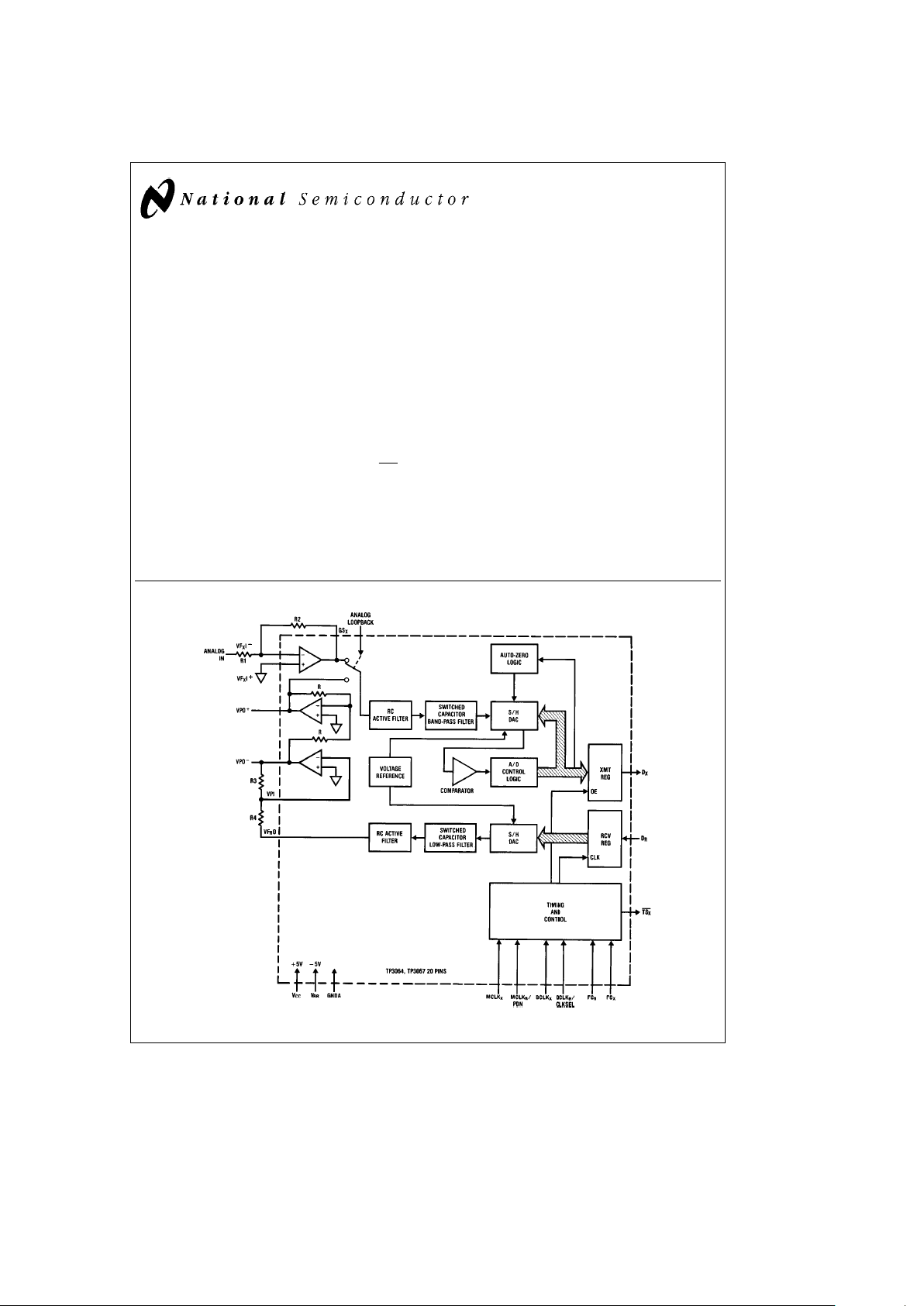
General Description
The TP3064 (m-law) and TP3067 (A-law) are monolithic
PCM CODEC/Filters utilizing the A/D and D/A conversion
architecture shown in
Figure 1
, and a serial PCM interface.
The devices are fabricated using National’s advanced double-poly CMOS process (microCMOS).
Similar to the TP305X family, these devices feature an additional Receive Power Amplifier to provide push-pull balanced output drive capability. The receive gain can be adjusted by means of two external resistors for an output level
of up to
g
6.6V across a balanced 600X load.
Also included is an Analog Loopback switch and a TS
X
out-
put.
See also AN-370, ‘‘Techniques for Designing with CODEC/
Filter COMBO Circuits.’’
COMBOÉand TRI-STATEÉare registered trademarks of National Semiconductor Corporation.
Features
Y
Complete CODEC and filtering system including:
Ð Transmit high-pass and low-pass filtering
Ð Receive low-pass filter with sin x/x correction
Ð Active RC noise filters
Ð m-law or A-law compatible COder and DECoder
Ð Internal precision voltage reference
Ð Serial I/O interface
Ð Internal auto-zero circuitry
Ð Receive push-pull power amplifiers
Y
m-lawÐTP3064
Y
A-lawÐTP3067
Y
Designed for D3/D4 and CCITT applications
Y
g
5V operation
Y
Low operating powerÐtypically 70 mW
Y
Power-down standby modeÐtypically 3 mW
Y
Automatic power-down
Y
TTL or CMOS compatible digital interfaces
Y
Maximizes line interface card circuit density
Block Diagram
TL/H/5070– 1
FIGURE 1
C
1995 National Semiconductor Corporation RRD-B30M115/Printed in U. S. A.
Page 2
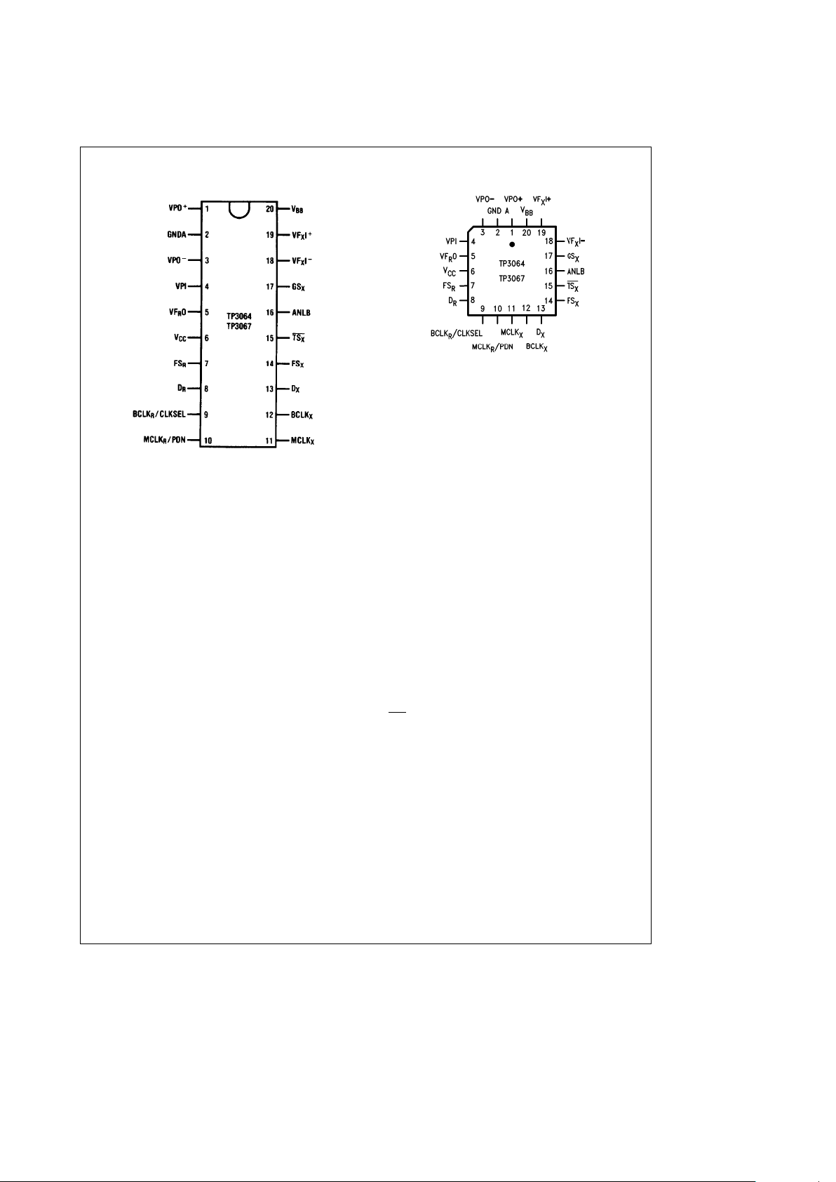
Connection Diagrams
Dual-In-Line Package
TL/H/5070– 2
Top View
Plastic Chip Carrier
TL/H/5070– 6
Top View
Order Number TP3064J or TP3067J
See NS Package J20A
Order Number TP3064WM or TP3067WM
See NS Package M20B
Order Number TP3064N or TP3067N
See NS Package N20A
Order Number TP3064V or TP3067V
See NS Package V20A
Pin Description
Symbol Function
VPO
a
The non-inverted output of the receive power
amplifier.
GNDA Analog ground. All signals are referenced to
this pin.
VPO
b
The inverted output of the receive power
amplifier.
VPI Inverting input to the receive power amplifier.
VF
R
O Analog output of the receive filter.
V
CC
Positive power supply pin. V
CC
ea
5Vg5%.
FS
R
Receive frame sync pulse which enables
BCLK
R
to shift PCM data into DR.FSRis an
8 kHz pulse train. See
Figures 2
and3for
timing details.
D
R
Receive data input. PCM data is shifted into
D
R
following the FSRleading edge.
BCLK
R
/ The bit clock which shifts data into DRafter
the FS
R
leading edge. May vary from 64 kHz
CLKSEL
to 2.048 MHz. Alternatively, may be a logic
input which selects either
1.536 MHz/1.544 MHz or 2.048 MHz for
master clock in synchronous mode and
BCLK
X
is used for both transmit and receive
directions (see Table I).
MCLK
R
/ Receive master clock. Must be 1.536 MHz,
1.544 MHz or 2.048 MHz. May be
PDN
asynchronous with MCLK
X
, but should be
synchronous with MCLK
X
for best
performance. When MCLK
R
is connected
continuously low, MCLK
X
is selected for all
internal timing. When MCLK
R
is connected
continuously high, the device is powered
down.
Symbol Function
MCLK
X
Transmit master clock. Must be 1.536 MHz,
1.544 MHz or 2.048 MHz. May be
asynchronous with MCLK
R
. Best
performance is realized from synchronous
operation.
BCLK
X
The bit clock which shifts out the PCM data
on D
X
. May vary from 64 kHz to 2.048 MHz,
but must be synchronous with MCLK
X
.
D
X
The TRI-STATEÉPCM data output which is
enabled by FS
X
.
FS
X
Transmit frame sync pulse input which
enables BCLK
X
to shift out the PCM data on
D
X
.FSXis an 8 kHz pulse train, see
Figures 2
and3for timing details.
TS
X
Open drain output which pulses low during
the encoder time slot.
ANLB Analog Loopback control input. Must be set
to logic ‘0’ for normal operation. When pulled
to logic ‘1’, the transmit filter input is
disconnected from the output of the transmit
preamplifier and connected to the VPO
a
output of the receive power amplifier.
GS
X
Analog output of the transmit input amplifier.
Used to externally set gain.
VF
X
I
b
Inverting input of the transmit input amplifier.
VF
X
I
a
Non-inverting input of the transmit input
amplifier.
V
BB
Negative power supply pin. V
BB
eb
5Vg5%.
2
Page 3
Functional Description
POWER-UP
When power is first applied, power-on reset circuitry initializes the COMBO
TM
and places it into a power-down state. All
non-essential circuits are deactivated and the D
X
,VFRO,
VPO
b
and VPOaoutputs are put in high impedance states.
To power-up the device, a logical low level or clock must be
applied to the MCLK
R
/PDN pin
and
FSXand/or FSRpulses
must be present. Thus, 2 power-down control modes are
available. The first is to pull the MCLK
R
/PDN pin high; the
alternative is to hold both FS
X
and FSRinputs continuously
lowÐthe device will power-down approximately 2 ms after
the last FS
X
or FSRpulse. Power-up will occur on the first
FS
X
or FSRpulse. The TRI-STATE PCM data output, DX,
will remain in the high impedance state until the second FS
X
pulse.
SYNCHRONOUS OPERATION
For synchronous operation, the same master clock and bit
clock should be used for both the transmit and receive directions. In this mode, a clock must be applied to MCLK
X
and the MCLKR/PDN pin can be used as a power-down
control. A low level on MCLK
R
/PDN powers up the device
and a high level powers down the device. In either case,
MCLK
X
will be selected as the master clock for both the
transmit and receive circuits. A bit clock must also be applied to BCLK
X
and the BCLKR/CLKSEL can be used to
select the proper internal divider for a master clock of 1.536
MHz, 1.544 MHz or 2.048 MHz. For 1.544 MHz operation,
the device automatically compensates for the 193rd clock
pulse each frame.
With a fixed level on the BCLK
R
/CLKSEL pin, BLCKXwill be
selected as the bit clock for both the transmit and receive
directions. Table I indicates the frequencies of operation
which can be selected, depending on the state of BCLK
R
/
CLKSEL. In this synchronous mode, the bit clock, BCLK
X
,
may be from 64 kHz to 2.048 MHz, but must be synchronous with MCLK
X
.
Each FSXpulse begins the encoding cycle and the PCM
data from the previous encode cycle is shifted out of the
enabled D
X
output on the positive edge of BCLKX. After 8
bit clock periods, the TRI-STATE D
X
output is returned to a
high impedance state. With an FS
R
pulse, PCM data is
latched via the D
R
input on the negative edge of BCLKX(or
BCLK
R
if running). FSXand FSRmust be synchronous with
MCLK
X/R
.
TABLE I. Selection of Master Clock Frequencies
Master Clock
BCLK
R
/CLKSEL
Frequency Selected
TP3067 TP3064
Clocked 2.048 MHz 1.536 MHz or
1.544 MHz
0 1.536 MHz or 2.048 MHz
1.544 MHz
1 2.048 MHz 1.536 MHz or
1.544 MHz
ASYNCHRONOUS OPERATION
For asynchronous operation, separate transmit and receive
clocks may be applied. MCLK
X
and MCLKRmust be 2.048
MHz for the TP3067, or 1.536 MHZ, 1.544 MHz for the
TP3064, and need not be synchronous. For best transmis-
sion performance, however, MCLK
R
should be synchronous
with MCLK
X
, which is easily achieved by applying only static
logic levels to the MCLK
R
/PDN pin. This will automatically
connect MCLK
X
to all internal MCLKRfunctions (see Pin
Description). For 1.544 MHz operation, the device automatically compensates for the 193rd clock pulse each frame.
FS
X
starts each encoding cycle and must be synchronous
with MCLK
X
and BCLKX.FSRstarts each decoding cycle
and must be synchronous with BCLK
R
. BCLKRmust be a
clock, the logic levels shown in Table I are not valid in asynchronous mode. BCLK
X
and BCLKRmay operate from 64
kHz to 2.048 MHz.
SHORT FRAME SYNC OPERATION
The COMBO can utilize either a short frame sync pulse (the
same as the TP3020/21 CODECs) or a long frame sync
pulse. Upon power initialization, the device assumes a short
frame mode. In this mode, both frame sync pulses, FS
X
and
FS
R
, must be one bit clock period long, with timing relation-
ships specified in
Figure 2
. With FSXhigh during a falling
edge of BCLK
X
, the next rising edge of BCLKXenables the
D
X
TRI-STATE output buffer, which will output the sign bit.
The following seven rising edges clock out the remaining
seven bits, and the next falling edge disables the D
X
output.
With FS
R
high during a falling edge of BCLKR(BCLKXin
synchronous mode), the next falling edge of BCLK
R
latches
in the sign bit. The following seven falling edges latch in the
seven remaining bits. All devices may utilize the short frame
sync pulse in synchronous or asynchronous operating
mode.
LONG FRAME SYNC OPERATION
To use the long (TP5116A/56 CODECs) frame mode, both
the frame sync pulses, FS
X
and FSR, must be three or more
bit clock periods long, with timing relationships specified in
Figure 3
. Based on the transmit frame sync, FSX, the COMBO will sense whether short or long frame sync pulses are
being used. For 64 kHz operation, the frame sync pulse
must be kept low for a minimum of 160 ns. The D
X
TRI-
STATE output buffer is enabled with the rising edge of FS
X
or the rising edge of BCLKX, whichever comes later, and the
first bit clocked out is the sign bit. The following seven
BCLK
X
rising edges clock out the remaining seven bits. The
D
X
output is disabled by the falling BCLKXedge following
the eighth rising edge, or by FS
X
going low, whichever
comes later. A rising edge on the receive frame sync pulse,
FS
R
, will cause the PCM data at DRto be latched in on the
next eight falling edges of BCLK
R
(BCLKXin synchronous
mode). All devices may utilize the long frame sync pulse in
synchronous or asynchronous mode.
TRANSMIT SECTION
The transmit section input is an operational amplifier with
provision for gain adjustment using two external resistors,
see
Figure 4
. The low noise and wide bandwidth allow gains
in excess of 20 dB across the audio passband to be realized. The op amp drives a unity-gain filter consisting of RC
active pre-filter, followed by an eighth order switched-capacitor bandpass filter clocked at 256 kHz. The output of
this filter directly drives the encoder sample-and-hold circuit.
The A/D is of companding type according to m-law
(TP3064) or A-law (TP3067) coding conventions. A precision voltage reference is trimmed in manufacturing to provide an input overload (t
MAX
) of nominally 2.5V peak (see
3
Page 4

Functional Description (Continued)
table of Transmission Characteristics). The FS
X
frame sync
pulse controls the sampling of the filter output, and then the
successive-approximation encoding cycle begins. The 8-bit
code is then loaded into a buffer and shifted out through D
X
at the next FSXpulse. The total encoding delay will be approximately 165 ms (due to the transmit filter) plus 125 ms
(due to encoding delay), which totals 290 ms. Any offset
voltage due to the filters or comparator is cancelled by sign
bit integration.
RECEIVE SECTION
The receive section consists of an expanding DAC which
drives a fifth order switched-capacitor low pass filter
clocked at 256 kHz. The decoder is A-law (TP3067) or
m-law (TP3064) and the 5th order low pass filter corrects for
the sin x/x attenuation due to the 8 kHz sample/hold. The
filter is then followed by a 2nd order RC active post-filter
with its output at VF
R
O. The receive section is unity-gain,
but gain can be added by using the power amplifiers. Upon
the occurrence of FS
R
, the data at the DRinput is clocked in
on the falling edge of the next eight BCLK
R
(BCLKX) peri-
ods. At the end of the decoder time slot, the decoding cycle
begins, and 10 ms later the decoder DAC output is updated.
The total decoder delay isE10 ms (decoder update) plus
110 ms (filter delay) plus 62.5 ms((/2 frame), which gives
approximately 180 ms.
RECEIVE POWER AMPLIFIERS
Two inverting mode power amplifiers are provided for directly driving a matched line interface transformer. The gain of
the first power amplifier can be adjusted to boost the
g
2.5V
peak output signal from the receive filter up to
g
3.3V peak
into an unbalanced 300X load, or
g
4.0V into an unbalanced 15 kX load. The second power amplifier is internally
connected in unity-gain inverting mode to give 6 dB of signal
gain for balanced loads.
Maximum power transfer to a 600X subscriber line termination is obtained by differentially driving a balanced transformer with a
S
2:1 turns ratio, as shown in
Figure 4
. A total
peak power of 15.6 dBm can be delivered to the load plus
termination.
ENCODING FORMAT AT D
X
OUTPUT
TP3064
TP3067
m-Law
A-Law
(Includes Even Bit Inversion)
V
IN
ea
Full-Scale 1 000000010101010
V
IN
e
0V 1 111111111010101
Ð0 111111101010101
V
IN
eb
Full-Scale 0 000000000101010
4
Page 5
Absolute Maximum Ratings
If Military/Aerospace specified devices are required,
please contact the National Semiconductor Sales
Office/Distributors for availability and specifications.
V
CC
to GNDA 7V
VBBto GNDA
b
7V
Voltage at any Analog Input
or Output V
CC
a
0.3V to V
BB
b
0.3V
Voltage at any Digital Input
or Output V
CC
a
0.3V to GNDAb0.3V
Operating Temperature Range
b
25§Ctoa125§C
Storage Temperature Range
b
65§Ctoa150§C
Lead Temp. (Soldering, 10 sec.) 300§C
ESD (Human Body Model) J 1000V
ESD (Human Body Model) N 1500V
Latch-Up Immunity 100 mA on Any Pin
Electrical Characteristics Unless otherwise noted, limits printed in BOLD characters are guaranteed for V
CC
e
a
5.0Vg5%, V
BB
eb
5.0Vg5%; T
A
e
0§Cto70§C by correlation with 100% electrical testing at T
A
e
25§C. All other limits
are assured by correlation with other production tests and/or product design and characterization. All signals referenced to
GNDA. Typicals specified at V
CC
ea
5.0V, V
BB
eb
5.0V, T
A
e
25§C.
Symbol Parameter Conditions Min Typ Max Units
POWER DISSIPATION (ALL DEVICES)
ICC0 Power-Down Current (Note) 0.5 1.5 mA
IBB0 Power-Down Current (Note) 0.05 0.3 mA
ICC1 Active Current VPIe0V; VFRO, VPOaand VPObunloaded 7.0 10.0 mA
IBB1 Active Current VPIe0V; VFRO, VPOaand VPObunloaded 7.0 10.0 mA
DIGITAL INTERFACE
V
IL
Input Low Voltage 0.6 V
V
IH
Input High Voltage 2.2 V
V
OL
Output Low Voltage DX,I
L
e
3.2 mA 0.4 V
TS
X,IL
e
3.2 mA, Open Drain 0.4 V
V
OH
Output High Voltage DX,I
H
eb
3.2 mA 2.4 V
I
IL
Input Low Current GNDAsV
IN
s
VIL, All Digital Inputs
b
10 10 mA
I
IH
Input High Current V
IH
s
V
IN
s
V
CC
b
10 10 mA
I
OZ
Output Current in High Impedance DX, GNDAsV
O
s
V
CC
b
10 10 mA
State (TRI-STATE)
Note: I
CC0
and I
BB0
are measured after first achieving a power-up state.
5
Page 6
Electrical Characteristics (Continued)
Unless otherwise noted, limits printed in BOLD characters are guaranteed for V
CC
ea
5.0Vg5%, V
BB
eb
5.0Vg5%; T
A
e
0§Cto70§C by correlation with 100% electrical testing at T
A
e
25§C. All other limits are assured by correlation with other
production tests and/or product design and characterization. All signals referenced to GNDA. Typicals specified at V
CC
e
a
5.0V, V
BB
eb
5.0V, T
A
e
25§C.
Symbol Parameter Conditions Min Typ Max Units
ANALOG INTERFACE WITH TRANSMIT INPUT AMPLIFIER (ALL DEVICES)
IIXA Input Leakage Current
b
2.5VsV
s
a
2.5V, VFXIaor VFXI
b
b
200 200 nA
RIXA Input Resistance
b
2.5VsV
s
a
2.5V, VFXIaor VFXI
b
10 MX
ROXA Output Resistance Closed Loop, Unity Gain 1 3 X
RLXA Load Resistance GS
X
10 kX
CLXA Load Capacitance GS
X
50 pF
VOXA Output Dynamic Range GSX,R
L
t
10 kX
b
2.8
a
2.8 V
AVXA Voltage Gain VFXIato GS
X
5000 V/V
FUXA Unity-Gain Bandwidth 1 2 MHz
VOSXA Offset Voltage
b
20 20 mV
VCMXA Common-Mode Voltage CMRRXAl60 dB
b
2.5 2.5 V
CMRRXA Common-Mode Rejection Ratio DC Test 60 dB
PSRRXA Power Supply Rejection Ratio DC Test 60 dB
ANALOG INTERFACE WITH RECEIVE FILTER (ALL DEVICES)
RORF Output Resistance Pin VFRO13X
R
L
RF Load Resistance VFRO
e
g
2.5V 10 kX
CLRF Load Capacitance Connect from VFRO to GNDA 25 pF
VOSRO Output DC Offset Voltage Measure from VFRO to GNDA
b
200 200 mV
ANALOG INTERFACE WITH POWER AMPLIFIERS (ALL DEVICES)
IPI Input Leakage Current
b
1.0VsVPIs1.0V
b
100 100 nA
RIPI Input Resistance
b
1.0VsVPIs1.0V 10 MX
VIOS Input Offset Voltage
b
25 25 mV
ROP Output Resistance Inverting Unity-Gain at 1 X
VPO
a
or VPO
b
F
C
Unity-Gain Bandwidth Open Loop (VPOb) 400 kHz
CLP Load Capacitance 100 pF
GA
P
a
Gain from VPObto VPO
a
R
L
e
600X VPOato VPO
b
b
1 V/V
Level at VPO
b
e
1.77 Vrms
PSRR
P
Power Supply Rejection of VPObConnected to VPI
V
CC
or V
BB
0 kHzb4 kHz 60 dB
4 kHz
b
50 kHz 36 dB
RLP Load Resistance Connect from VPOato VPO
b
600 X
6
Page 7

Timing Specifications
Unless otherwise noted, limits printed in BOLD characters are guaranteed for V
CC
ea
5.0Vg5%, V
BB
eb
5.0Vg5%, T
A
e
0§Cto70§C by correlation with 100% electrical testing at T
A
e
25§C. All other limits are assured by correlation with other
production tests and/or product design and characterization. All signals are referenced to GNDA. Typicals specified at V
CC
e
a
5.0V, V
BB
eb
5.0V, T
A
e
25§C. All timing parameters are measured at V
OH
e
2.0V and V
OL
e
0.7V.
See Definitions and Timing Conventions section for test methods information.
Symbol Parameter Conditions Min Typ Max Units
1/t
PM
Frequency of Master Clock 1.536 MHz
1.544 MHz
MCLK
X
and MCLK
R
2.048 MHz
t
RM
Rise Time of Master Clock MCLKXand MCLK
R
50 ns
t
FM
Fall Time of Master Clock MCLKXand MCLK
R
50 ns
t
PB
Period Bit of Clock 485 488 15725 ns
t
RB
Rise Time of Bit Clock BCLKXand BCLK
R
50 ns
t
FB
Fall Time of Bit Clock BCLKXand BCLK
R
50 ns
t
WMH
Width of Master Clock High MCLKXand MCLK
R
160 ns
t
WML
Width of Master Clock Low MCLKXand MCLK
R
160 ns
t
SBFM
Set-Up Time from BCLKXHigh 100 ns
to MCLK
X
Falling Edge
t
SFFM
Set-Up Time from FSXHigh Long Frame Only 100 ns
to MCLK
X
Falling Edge
t
WBH
Width of Bit Clock High 160 ns
t
WBL
Width of Bit Clock Low 160 ns
t
HBFL
Holding Time from Bit Clock Long Frame Only 0 ns
Low to Frame Sync
t
HBFS
Holding Time from Bit Clock Short Frame Only 0 ns
High to Frame Sync
t
SFB
Set-Up Time for Frame Sync Long Frame Only 80 ns
to Bit Clock Low
t
DBD
Delay Time from BCLKXHigh Loade150 pF plus 2 LSTTL Loads 0 180 ns
to Data Valid
t
DBTS
Delay Time to TSXLow Loade150 pF plus 2 LSTTL Loads 140 ns
t
DZC
Delay Time from BCLKXLow to 50 165 ns
Data Output Disabled
t
DZF
Delay Time to Valid Data from C
L
e
0 pF to 150 pF 20 165 ns
FS
X
or BCLKX, Whichever
Comes Later
t
SDB
Set-Up Time from DRValid to 50 ns
BCLK
R/X
Low
t
HBD
Hold Time from BCLK
R/X
Low to 50 ns
D
R
Invalid
t
SF
Set-Up Time from FS
X/R
to Short Frame Sync Pulse (1 Bit Clock 50 ns
BCLK
X/R
Low Period Long)
t
HF
Hold Time from BCLK
X/R
Low Short Frame Sync Pulse (1 Bit Clock 100 ns
to FS
X/R
Low Period Long)
t
HBFI
Hold Time from 3rd Period of Long Frame Sync Pulse (from 3 to 8 Bit 100 ns
Bit Clock Low to Frame Sync Clock Periods Long)
(FS
X
or FSR)
t
WFL
Minimum Width of the Frame 64k Bit/s Operating Mode 160 ns
Sync Pulse (Low Level)
7
Page 8

Timing Diagrams
TL/H/5070– 3
FIGURE 2. Short Frame Sync Timing
8
Page 9

Timing Diagrams (Continued)
TL/H/5070– 4
FIGURE 3. Long Frame Sync Timing
9
Page 10

Transmission Characteristics
Unless otherwise noted, limits printed in BOLD characters are guaranteed for V
CC
ea
5.0Vg5%, V
BB
eb
5.0Vg5%; T
A
e
0§Cto70§C by correlation with 100% electrical testing at T
A
e
25§C. All other limits are assured by correlation with other
production tests and/or product design and characterization. GNDA
e
0V, fe1.02 kHz, V
IN
e
0 dbm0, transmit input amplifier
connected for unity gain non-inverting. Typicals specified at V
CC
ea
5.0V, V
BB
eb
5.0V, T
A
e
25§C.
Symbol Parameter Conditions Min Typ Max Units
AMPLITUDE RESPONSE
Absolute Levels Nominal 0 dBm0 Level is 4 dBm
(Definition of (600X)
nominal gain) 0 dBm0 1.2276 Vrms
t
MAX
Virtual Decision Value Defined Max Transmit Overload Level
per CCITT Rec. G711 TP3064 (3.17 dBm0) 2.501 V
PK
TP3067 (3.14 dBm0) 2.492 V
PK
G
XA
Transmit Gain, Absolute T
A
e
25§C, V
CC
e
5V, V
BB
eb
5V
b
0.15 0.15 dB
G
XR
Transmit Gain, Relative to G
XA
fe16 Hz
b
40 dB
f
e
50 Hz
b
30 dB
f
e
60 Hz
b
26 dB
f
e
200 Hz
b
1.8
b
0.1 dB
f
e
300 Hz-3000 Hz
b
0.15 0.15 dB
f
e
3300 Hz
b
0.35 0.05 dB
f
e
3400 Hz
b
0.7 0 dB
fe4000 Hz
b
14 dB
f
e
4600 Hz and Up, Measure
b
32 dB
Response from 0 Hz to 4000 Hz
G
XAT
Absolute Transmit Gain Variation Relative to G
XA
b
0.1 0.1 dB
with Temperature
G
XAV
Absolute Transmit Gain Variation Relative to G
XA
b
0.05 0.05 dB
with Supply Voltage
G
XRL
Transmit Gain Variations with Sinusoidal Test Method
Level Reference Level
eb
10 dBm0
VF
X
I
a
eb
40 dBm0 toa3 dBm0
b
0.2 0.2 dB
VF
X
I
a
eb
50 dBm0 tob40 dBm0
b
0.4 0.4 dB
VF
X
I
a
eb
55 dBm0 tob50 dBm0
b
1.2 1.2 dB
G
RA
Receive Gain, Absolute T
A
e
25§C, V
CC
e
5V, V
BB
eb
5V
b
0.15 0.15 dB
Input
e
Digital Code Sequence
for 0 dBm0 Signal
G
RR
Receive Gain, Relative to G
RA
fe0 Hz to 3000 Hz
b
0.15 0.15 dB
f
e
3300 Hz
b
0.35 0.05 dB
f
e
3400 Hz
b
0.7 0 dB
f
e
4000 Hz
b
14 dB
G
RAT
Absolute Receive Gain Variation Relative to G
RA
b
0.1 0.1 dB
with Temperature
G
RAV
Absolute Receive Gain Variation Relative to G
RA
b
0.05 0.05 dB
with Supply Voltage
G
RRL
Receive Gain Variations with Sinusoidal Test Method; Reference
Level Input PCM Code Corresponds to an
Ideally Encoded
b
10 dBm0 Signal
PCM Level
eb
40 dBm0 toa3 dBm0
b
0.2 0.2 dB
PCM Level
eb
50 dBm0 tob40 dBm0
b
0.4 0.4 dB
PCM Level
eb
55 dBm0 tob50 dBm0
b
1.2 1.2 dB
V
RO
Receive Filter Output at VFRORL
e
10 kX
b
2.5 2.5 V
10
Page 11

Transmission Characteristics (Continued)
Unless otherwise noted, limits printed in BOLD characters are guaranteed for V
CC
ea
5.0Vg5%, V
BB
eb
5.0Vg5%; T
A
e
0§Cto70§C by correlation with 100% electrical testing at T
A
e
25§C. All other limits are assured by correlation with other
production tests and/or product design and characterization. GNDA
e
0V, fe1.02 kHz, V
IN
e
0 dbm0, transmit input amplifier
connected for unity gain non-inverting. Typicals specified at V
CC
ea
5.0V, V
BB
eb
5.0V, T
A
e
25§C.
Symbol Parameter Conditions Min Typ Max Units
ENVELOPE DELAY DISTORTION WITH FREQUENCY
D
XA
Transmit Delay, Absolute fe1600 Hz 290 315 ms
D
XR
Transmit Delay, Relative to D
XA
fe500 Hzb600 Hz 195 220 ms
f
e
600 Hzb800 Hz 120 145 ms
f
e
800 Hzb1000 Hz 50 75 ms
f
e
1000 Hzb1600 Hz 20 40 ms
f
e
1600 Hzb2600 Hz 55 75 ms
f
e
2600 Hzb2800 Hz 80 105 ms
fe2800 Hzb3000 Hz 130 155 ms
D
RA
Receive Delay, Absolute fe1600 Hz 180 200 ms
D
RR
Receive Delay, Relative to D
RA
fe500 Hzb1000 Hz
b
40
b
25 ms
f
e
1000 Hzb1600 Hz
b
30
b
20 ms
f
e
1600 Hzb2600 Hz 70 90 ms
f
e
2600 Hzb2800 Hz 100 125 ms
f
e
2800 Hzb3000 Hz 145 175 ms
NOISE
N
XC
Transmit Noise, C Message TP3064 (Note 1) 12 15 dBrnC0
Weighted
N
XP
Transmit Noise, Psophometric TP3067 (Note 1)
b
74
b
67 dBm0p
Weighted
N
RC
Receive Noise, C Message PCM Code Equals Alternating
Weighted Positive and Negative Zero
TP3064 8 11 dBrnCO
N
RP
Receive Noise, Psophometric PCM Code Equals Positive
Weighted Zero
TP3067
b
82
b
79 dBm0p
N
RS
Noise, Single Frequency fe0 kHz to 100 kHz, Loop Around
b
53 dBm0
Measurement, VF
X
I
a
e
0 Vrms
PPSR
X
Positive Power Supply Rejection, V
CC
e
5.0 V
DC
a
100 mVrms
Transmit fe0 kHzb50 kHz (Note 2) 40 dBC
NPSR
X
Negative Power Supply Rejection, V
BB
eb
5.0 V
DC
a
100 mVrms
Transmit f
e
0 kHzb50 kHz (Note 2) 40 dBC
PPSR
R
Positive Power Supply Rejection, PCM Code Equals Positive Zero
Receive V
CC
e
5.0 V
DC
a
100 mVrms
Measure VF
R
O
f
e
0Hzb4000 Hz 38 dBC
f
e
4 kHzb50 kHz 25 dB
NPSR
R
Negative Power Supply Rejection, PCM Code Equals Positive Zero
Receive V
BB
eb
5.0 V
DC
a
100 mVrms
Measure VF
R
O
f
e
0Hzb4000 Hz 40 dBC
f
e
4 kHzb25 kHz 40 dB
f
e
25 kHzb50 kHz 36 dB
SOS Spurious Out-of-Band Signals 0 dBm0, 300 Hzb3400 Hz Input
at the Channel Output PCM Code Applied at DR
Measure Individual Image Signals at
VF
R
O
4600 Hz–7600 Hz
b
32 dB
7600 Hz–8400 Hz
b
40 dB
8400 Hz–100,000 Hz
b
32 dB
11
Page 12

Transmission Characteristics (Continued)
Unless otherwise noted, limits printed in BOLD characters are guaranteed for V
CC
ea
5.0Vg5%, V
BB
eb
5.0Vg5%; T
A
e
0§Cto70§C by correlation with 100% electrical testing at T
A
e
25§C. All other limits are assured by correlation with other
production tests and/or product design and characterization. GNDA
e
0V, fe1.02 kHz, V
IN
e
0 dbm0, transmit input amplifier
connected for unity gain non-inverting. Typicals specified at V
CC
ea
5.0V, V
BB
eb
5.0V, T
A
e
25§C.
Symbol Parameter Conditions Min Typ Max Units
DISTORTION
STD
X,
Signal to Total Distortion Sinusoidal Test Method (Note 3)
STD
R
Transmit or Receive Levele3.0 dBm0 33 dBC
Half-Channel
e
0 dBm0 tob30 dBm0 36 dBC
eb
40 dBm0 XMT 29 dBC
RCV 30 dBC
eb
55 dBm0 XMT 14 dBC
RCV 15 dBC
SFD
X
Single Frequency Distortion,
b
46 dB
Transmit
SFD
R
Single Frequency Distortion,
b
46 dB
Receive
IMD Intermodulation Distortion Loop Around Measurement,
b
41 dB
VF
X
I
a
eb
4 dBm0 tob21 dBm0, Two
Frequencies in the Range
300 Hz
b
3400 Hz
CROSSTALK
CT
X-R
Transmit to Receive Crosstalk fe300 Hzb3000 Hz
D
R
e
Quiet PCM Code
b
90b75 dB
CT
R-X
Receive to Transmit Crosstalk fe300 Hzb3000 Hz, VFXIe0V
b
90b70 dB
(Note 2)
POWER AMPLIFIERS
VOPA Maximum 0 dBm0 Level Balanced Load, RLConnected Between
(Better than
g
0.1 dB Linearity over VPOaand VPOb.
the Range
b
10 dBm0 toa3 dBm0) R
L
e
600X 3.3 Vrms
R
L
e
1200X 3.5 Vrms
S/D
P
Signal/Distortion R
L
e
600X 50 dB
Note 1: Measured by extrapolation from the distortion test result atb50 dBm0.
Note 2: PPSR
X
, NPSRX, and CT
RbX
are measured with ab50 dBm0 activation signal applied to VFXIa.
Note 3: TP3064 is measured using C message weighted filter. TP3067 is measured using psophometric weighted filter.
12
Page 13

Applications Information
POWER SUPPLIES
While the pins of the TP3060 family are well protected
against electrical misuse, it is recommended that the standard CMOS practice be followed, ensuring that ground is
connected to the device before any other connections are
made. In applications where the printed circuit board may be
plugged into a ‘‘hot’’ socket with power and clocks already
present, an extra long ground pin in the connector should
be used.
All ground connections to each device should meet at a
common point as close as possible to the GNDA pin. This
minimizes the interaction of ground return currents flowing
through a common bus impedance. 0.1 mF supply decoupling capacitors should be connected from this common
ground point to V
CC
and VBB, as close to the device as
possible.
For best performance, the ground point of each CODEC/
FILTER on a card should be connected to a common card
ground in ‘‘STAR’’ formation, rather than via a ground bus.
This common ground point should be decoupled to V
CC
and
V
BB
with 10 mF capacitors.
Note: See Application Note 370 for further details
Typical Asynchronous Application
TL/H/5070– 5
Note 1: Transmit gaine20clog
#
R1aR2
R2
J
,(R1aR2)t10 kX
Note 2: Receive gain
e
20clog
#
2cR3
R4
J
,R4t10 kX
FIGURE 4
13
Page 14

Definitions and Timing Conventions
DEFINITIONS
V
IH
VIHis the d.c. input level above which
an input level is guaranteed to appear
as a logical one. This parameter is to
be measured by performing a
functional test at reduced clock
speeds and nominal timing, (i.e. not
minimum setup and hold times or
output strobes), with the high level of
all driving signals set to V
IH
and
maximum supply voltages applied to
the device
V
IL
VILis the d.c. input level below which
an input level is guaranteed to appear
as a logical zero to the device. This
parameter is measured in the same
manner as V
IH
but with all driving
signal low levels set to V
IL
and
minimum supply voltages applied to
the device.
V
OH
VOHis the minimum d.c. output level
to which an output placed in a logical
one state will converge when loaded
at the maximum specified load current.
V
OL
VOLis the maximum d.c. output level
to which an output placed in a logical
zero state will converge when loaded
at the maximum specified load current.
Threshold Region The threshold region is the range of
input voltages between V
IL
and VIH.
Valid Signal A signal is Valid if it is in one of the
valid logic states, (i.e. above V
IH
or
below V
IL
). In timing specifiations, a
signal is deemed valid at the instant it
enters a valid state.
Invalid Signal A signal is Invalid if it is not in a valid
logic state, i.e. when it is in in the
threshold region between V
IL
and VIH.
In timing specifications, a signal is
deemed Invalid at the instant it enters
the threshold region.
TIMING CONVENTIONS
For the purposes of this timing specification, the following
conventions apply:
Input Signals All input signals may be characterized
as: V
L
e
0.4V, V
H
e
2.4V, t
R
k
10 ns,
t
F
k
10 ns.
Period The period of clock signal is
designated as t
Pxx
where xx
represents the mnemonic of the clock
signal being specified.
Rise Time Rise times are designated as t
Ryy
,
where yy represents a mnemonic of
the signal whose rise time is being
specified. t
Ryy
is measured from VILto
V
IH
.
Fall Time Fall times are designated as t
Fyy
,
where yy represents a mnemonic of
the signal whose fall time is being
specified. t
Fyy
is measured from VIHto
V
IL
.
Pulse Width High The high pulse width is designated as
t
WzzH
, where zz represents the
mnemonic of the input or output signal
whose pulse width is being specified.
High pulse widths are measured from
V
IH
to VIH.
Pulse Width Low The low pulse width is designated as
t
WzzL
, where zz represents the
mnemonic of the input or output signal
whose pulse width is being specified.
Low pulse widths are measured from
V
IL
to VIL.
Setup Time Setup times are designated as t
Swwxx
,
where ww represents the mnemonic of
the input signal whose setup time is
being specified relative to a clock or
strobe input represented by mnemonic
xx. Setup times are measured from the
ww Valid to xx Invalid.
Hold Time Hold times are designated as t
Hxxww
,
where ww represents the mnemonic of
the input signal whose hold time is
being specified relative to a clock or
strobe input represented by mnemonic
xx. Hold times are measured from xx
Valid to ww Invalid.
Delay Time Delay times are designated as t
Dxxyy
Hi to Low, where xx represents the
mnemonic of the input reference
signal and yy represents the
mnemonic of the output signal whose
timing is being specified relative to xx.
The mnemonic may optionally be
terminated by an H or L to specify the
high going or low going transition of
the output signal. Maximum delay
times are measured from xx Valid to yy
Valid. Minimum delay times are
measured from xx Valid to yy Invalid.
This parameter is tested under the
load conditions specified in the
Conditions column of the Timing
Specifications section of this data
sheet.
14
Page 15

15
Page 16

Physical Dimensions inches (millimeters)
Cavity Dual-In-Line Package (J)
Order Number TP3064J or TP3067J
NS Package Number J20A
Molded Small Outline Package (WM)
Order Number TP3064WM or TP3067WM
NS Package Number M20B
16
Page 17

Physical Dimensions inches (millimeters) (Continued)
Molded Dual-In-Line Package (N)
Order Number TP3064N or TP3067N
NS Package Number N20A
17
Page 18

TP3064, TP3067 ‘‘Enhanced’’ Serial Interface CMOS CODEC/Filter COMBO
Physical Dimensions inches (millimeters) (Continued) Lit.
Ý
113975
Plastic Chip Carrier (V)
Order Number TP3064V or TP3067V
NS Package Number V20A
LIFE SUPPORT POLICY
NATIONAL’S PRODUCTS ARE NOT AUTHORIZED FOR USE AS CRITICAL COMPONENTS IN LIFE SUPPORT
DEVICES OR SYSTEMS WITHOUT THE EXPRESS WRITTEN APPROVAL OF THE PRESIDENT OF NATIONAL
SEMICONDUCTOR CORPORATION. As used herein:
1. Life support devices or systems are devices or 2. A critical component is any component of a life
systems which, (a) are intended for surgical implant support device or system whose failure to perform can
into the body, or (b) support or sustain life, and whose be reasonably expected to cause the failure of the life
failure to perform, when properly used in accordance support device or system, or to affect its safety or
with instructions for use provided in the labeling, can effectiveness.
be reasonably expected to result in a significant injury
to the user.
National Semiconductor National Semiconductor National Semiconductor National Semiconductor
Corporation Europe Hong Kong Ltd. Japan Ltd.
1111 West Bardin Road Fax: (
a
49) 0-180-530 85 86 13th Floor, Straight Block, Tel: 81-043-299-2309
Arlington, TX 76017 Email: cnjwge@tevm2.nsc.com Ocean Centre, 5 Canton Rd. Fax: 81-043-299-2408
Tel: 1(800) 272-9959 Deutsch Tel: (
a
49) 0-180-530 85 85 Tsimshatsui, Kowloon
Fax: 1(800) 737-7018 English Tel: (
a
49) 0-180-532 78 32 Hong Kong
Fran3ais Tel: (
a
49) 0-180-532 93 58 Tel: (852) 2737-1600
Italiano Tel: (
a
49) 0-180-534 16 80 Fax: (852) 2736-9960
National does not assume any responsibility for use of any circuitry described, no circuit patent licenses are implied and National reserves the right at any time without notice to change said circuitry and specifications.
 Loading...