

Page 1
TLC8188
10-BIT, 4 MSPS, CIS/LINEAR CCD SENSOR PROCESSOR
SLAS177A – DECEMBER 1997 – REVISED SEPTEMBER 1998
1
POST OFFICE BOX 655303 • DALLAS, TEXAS 75265
D
Supports Both CIS and CCD Sensors
D
10-Bit, 4 MSPS, A/D Converter
D
Differential Nonlinearity Error: ±0.5 LSB Typ
D
Integral Nonlinearity Error: ±0.6 LSB Typ
D
8-Bit Offset Correction DAC
D
PGA With 6-Bit Gain Resolution
D
Auto-cycling Gain and Offset Control
D
Single 5-V Supply Operation
D
Very Low Power: 190 mW Typical
D
Control by Parallel and Serial Interface
D
Internal Reference Voltages
D
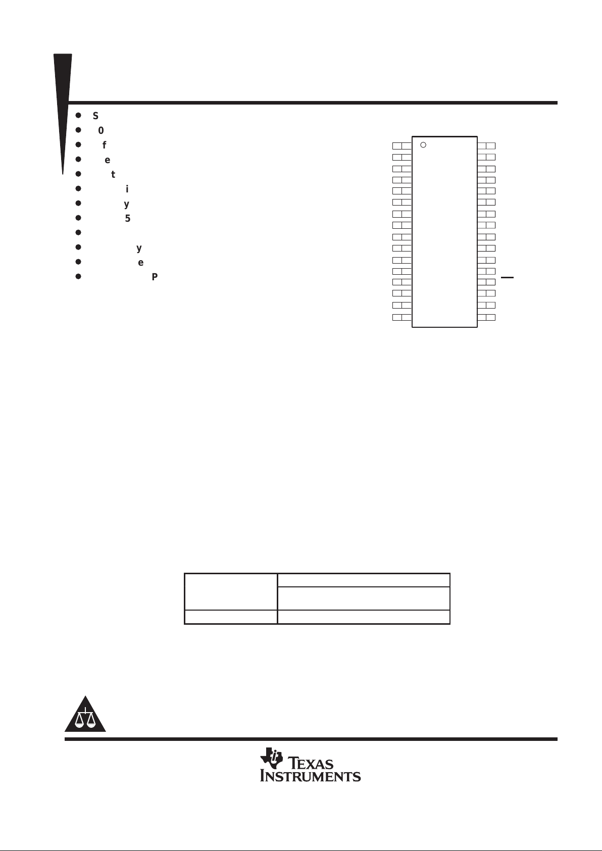
32-Pin TSSOP Package
description
The TLC8188 is a highly-integrated monolithic
analog signal processor/digitizer designed to
interface the contact image sensor (CIS) and linear charge-coupled device (CCD) image sensors in scanner
applications. The input of the TLC8188 allows direct connection to the CIS and direct ac coupling of the linear
CCD. The TLC8188 performs all the analog processing functions necessary to maximize the dynamic range,
correct various errors associated with the CIS and the linear CCD sensors, and then digitize the results with an
on-chip analog-to-digital converter (ADC). The key components of the TLC8188 include: input clamp circuitry
and a correlated double sampler (CDS), a programmable gain amplifier (PGA) with auto-cycling gain control, a
programmable offset correction controlled by a digital-to-analog converter (DAC), a 10-bit, 4 MSPS pipeline
ADC, a bidirectional parallel bus and a three-wire serial port for easy microprocessor interface, and internal
reference voltages.
Designed in advanced CMOS process, the TLC8188 operates from a single 5-V power supply and its digital
interface is 3 V compatible. The normal power consumption of the TLC8188 is just 190 mW.
Fully integrated analog processing circuitry , high throughput rate, single supply operation and low cost make the
TLC8188 an ideal CIS/linear CCD sensor interfacing solution for imaging applications such as scanners and
multifunctional office equipment (printer/scanner/facsimile/copier).
The device is available in a 32-pin TSSOP package and is specified over the 0°C to 70°C operating temperature
range.
AVAILABLE OPTIONS
PACKAGED DEVICE
T
A
SMALL OUTLINE
(DA)
0°C to 70°C TLC8188CDA
Copyright 1998, Texas Instruments Incorporated
PRODUCTION DATA information is current as of publication date.
Products conform to specifications per the terms of Texas Instruments
standard warranty. Production processing does not necessarily include
testing of all parameters.
Please be aware that an important notice concerning availability, standard warranty, and use in critical applications of
Texas Instruments semiconductor products and disclaimers thereto appears at the end of this data sheet.
1
2
3
4
5
6
7
8
9
10
11
12
13
14
15
16
32
31
30
29
28
27
26
25
24
23
22
21
20
19
18
17
OP0
OP1
OP2
OP3
OP4
DIV
DD
DIGND
OP5
OP6
OP7
OP8
OP9
DV
DD
DGND
ADCCLK
SCK/RNW
RPO
RMO
RIN
GIN
BIN
AV
DD
AGND
CLAMP
SR
SV
MA0/ACYC
MA1
OE
NRESET
SEN/STB
SDI/DNA
DA PACKAGE
(TOP VIEW)
Page 2
TLC8188
10-BIT, 4 MSPS, CIS/LINEAR CCD SENSOR PROCESSOR
SLAS177A – DECEMBER 1997 – REVISED SEPTEMBER 1998
2
POST OFFICE BOX 655303 • DALLAS, TEXAS 75265
functional block diagram
8-BIT
DAC
CLAMP
Control
Logic
MUX
RIN
MUX
GRN
OS
BLUE
OS
RED
OS
CDS
(S/H)
PGA
MUX
GRN
GAIN
BLUE
GAIN
RED
GAIN
10-BIT
ADC
THREE
STATE
LATCHES
ADCCLK
SV
MA0/ACYC
MA1
SR
NRESET
SDI/DNA
SCK/RNW
SEN/STB
SERIAL
PORT
8
6
INTERNAL
REFERENCE
OP (0 – 9)
OE
CLAMP RPO RMOAV
DD
DV
DD
DIV
DD
AGND DGND DIGND
GIN
BIN
Page 3
TLC8188
10-BIT, 4 MSPS, CIS/LINEAR CCD SENSOR PROCESSOR
SLAS177A – DECEMBER 1997 – REVISED SEPTEMBER 1998
3
POST OFFICE BOX 655303 • DALLAS, TEXAS 75265
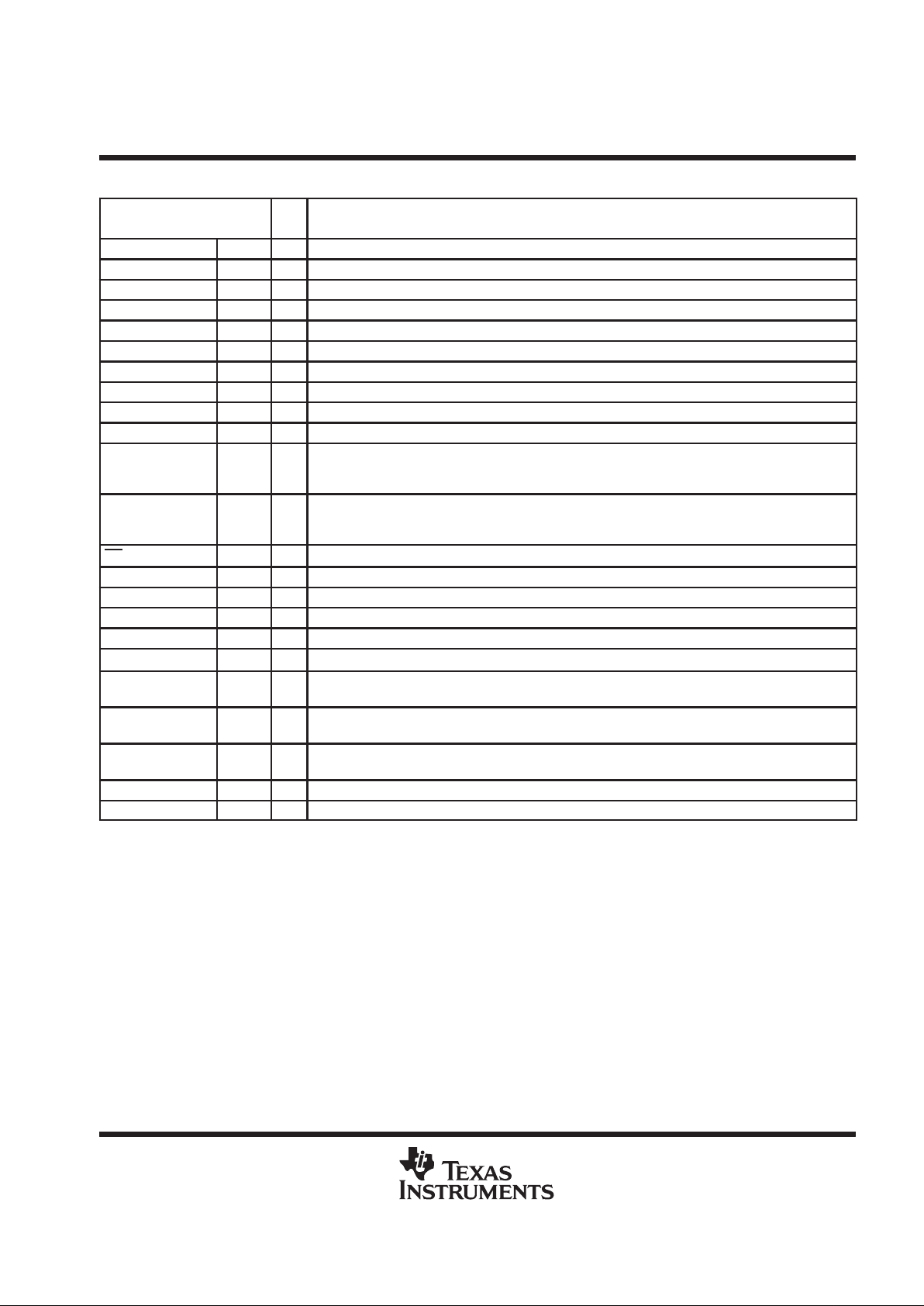
Terminal Functions
TERMINAL
NAME NO.
I/O
DESCRIPTION
ADCCLK 15 I ADC conversion clock input.
AGND 26 Analog ground
AV
DD
27 Analog supply voltage, 5 V
BIN 28 I Blue channel input
CLAMP 25 I CCD input clamp signal, active high
DGND 14 Digital ground
DIGND 7 Digital interface circuit ground
DIV
DD
6 Digital interface circuit supply voltage, 3 V to 5 V
DV
DD
13 Digital supply voltage, 5 V
GIN 29 I Green channel input
MA1, MA0/ACYC 21, 22 I MA1 and MA0 select the color to which all internal MUX (input, gain, offset) will point. When in
auto-cycling mode, the input mux and internal registers are auto-cycled by the ACYC. The ACYC is a
control signal such as a line start pulse that defines the start of a current scanning line.
NRESET 19 I Power-on reset and Interface mode control. If SEN/STB is 1 when NRESET goes high then the device
is in parallel configuration data input mode. If SEN/STB is 0 when NRESET goes high then the device
is in serial data input mode.
OE
20 I Three-state output enable, active low
OP(0–4) 1 – 5 I/O Three-state bi-directional data bus, OP0 and OP1 are output only.
OP(5–9) 8 – 12 I/O Three-state bi-directional data bus.
RIN 30 I Red channel input
RMO 31 O Ref– output for external decoupling
RPO 32 O Ref+ output for external decoupling
SCK/RNW 16 I Serial interface: serial clock
Parallel interface: 1 – OP(9–2) is output bus, 0 – OP(9–2) is input bus
SDI/DNA 17 I Serial interface: serial interface input data
Parallel interface: 1 – data, 0 – address
SEN/STB 18 I Serial interface: serial data transfer enable, active high.
Parallel interface: strobe, active low.
SR 24 I CCD reset level sample pulse input
SV 23 I CCD signal level sample pulse input
absolute maximum ratings over operating free-air temperature (unless otherwise noted)
†
Supply voltage range, V
CC
–0.3 V to 6.5 V. . . . . . . . . . . . . . . . . . . . . . . . . . . . . . . . . . . . . . . . . . . . . . . . . . . . . . . .
Analog input voltage range –0.3 V to V
CC
+0.3 V. . . . . . . . . . . . . . . . . . . . . . . . . . . . . . . . . . . . . . . . . . . . . . . . . . . .
Reference input voltage V
CC
+0.3 V. . . . . . . . . . . . . . . . . . . . . . . . . . . . . . . . . . . . . . . . . . . . . . . . . . . . . . . . . . . . . .
Digital input voltage range –0.3 V to V
CC
+0.3 V. . . . . . . . . . . . . . . . . . . . . . . . . . . . . . . . . . . . . . . . . . . . . . . . . . . .
Operating
virtual junction temperature range, T
J
–40°C to 150°C. . . . . . . . . . . . . . . . . . . . . . . . . . . . . . . . . . . . .
Operating free-air temperature range, T
A
0°C to 70°C. . . . . . . . . . . . . . . . . . . . . . . . . . . . . . . . . . . . . . . . . . . . . .
Storage temperature range, T
stg
–65°C to 150°C. . . . . . . . . . . . . . . . . . . . . . . . . . . . . . . . . . . . . . . . . . . . . . . . . . .
Lead temperature 1,6 mm (1/16 inch) from case for 10 seconds 260°C. . . . . . . . . . . . . . . . . . . . . . . . . . . . . . .
†
Stresses beyond those listed under “absolute maximum ratings” may cause permanent damage to the device. These are stress ratings only, and
functional operation of the device at these or any other conditions beyond those indicated under “recommended operating conditions” is not
implied. Exposure to absolute-maximum-rated conditions for extended periods may affect device reliability.
Page 4
TLC8188
10-BIT, 4 MSPS, CIS/LINEAR CCD SENSOR PROCESSOR
SLAS177A – DECEMBER 1997 – REVISED SEPTEMBER 1998
4
POST OFFICE BOX 655303 • DALLAS, TEXAS 75265
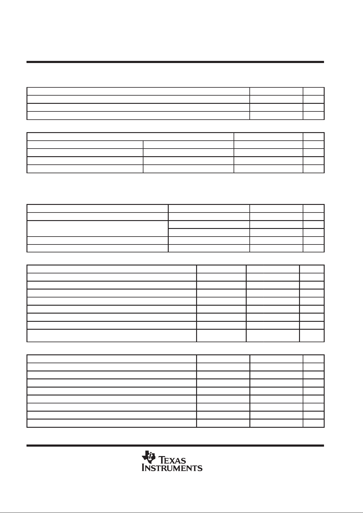
recommended operating conditions
power supplies
MIN NOM MAX UNIT
Analog supply voltage, A V
DD
4.5 5.5 V
Digital supply voltage, DV
DD
4.5 5.5 V
Digital interface supply voltage, DIV
DD
2.7 5.5 V
digital inputs
MIN NOM MAX UNIT
High-level input voltage, V
IH
DIVDD = 3 V to 5.5 V 0.8DIV
DD
V
Low-level input voltage, V
IL
DIVDD = 3 V to 5.5 V 0.2DIV
DD
V
Input ADCCLK frequency 4 MHz
Input SCLK frequency 13.3 MHz
electrical characteristics over recommended operating free-air temperature range,
AV
DD
= DVDD = 5 V, ADCCLK = 4 MHz (unless otherwise noted)
total device
PARAMETER TEST CONDITIONS
MIN TYP MAX UNIT
AVDD operating current 35 40 mA
p
1 mA
DIV
DD
operating current
5 pF loading, all outputs switching 2 mA
Device power consumption 190 mW
Device power consumption, power down mode 7 mW
analog-to-digital converter (ADC)
PARAMETER TEST CONDITIONS MIN TYP MAX UNIT
Resolution 10 Bits
INL Integral nonlinearity ±0.6 ±2 LSB
DNL Differential nonlinearity ±0.5 ±1 LSB
No missing codes
Full-scale input voltage 4 V
PP
Input capacitance 15 pF
Conversion rate 4 MHz
ADC output latency 4
ADCCLK
cycles
correlated double sampler (CDS) and programmable gain amplifier (PGA)
PARAMETER TEST CONDITIONS MIN TYP MAX UNIT
CDS sample rate 4 MHz
Analog input voltage 4 V
Input capacitance 5 pF
PGA gain control resolution 6 Bits
PGA gain 1 5 V/V
PGA gain accuracy ±5%
PGA output settling time 125 ns
New gain settling time 125 ns
Page 5

TLC8188
10-BIT, 4 MSPS, CIS/LINEAR CCD SENSOR PROCESSOR
SLAS177A – DECEMBER 1997 – REVISED SEPTEMBER 1998
5
POST OFFICE BOX 655303 • DALLAS, TEXAS 75265
electrical characteristics over recommended operating free-air temperature range,
AV
DD
= DVDD = 5 V, ADCCLK = 4 MHz (unless otherwise noted) (continued)
digital-to-analog converter (DAC)
PARAMETER TEST CONDITIONS MIN TYP MAX UNIT
Resolution 8 Bits
INL Integral nonlinearity ±0.5 ±1 LSB
DNL Differential nonlinearity ±0.3 ±1 LSB
Output settling time To 1% accuracy 2 µs
reference voltages
PARAMETER TEST CONDITIONS MIN TYP MAX UNIT
Internal bandgap voltage reference 1.15 1.22 1.28 V
T emperature coef ficient 100 ppm/°C
Voltage reference noise 0.5 LSB
ADCRef+ ADC positive reference voltage Externally decoupled 3.35 3.5 3.65 V
ADCRef– ADC negative reference voltage Externally decoupled 1.35 1.5 1.65 V
DACRef+ DAC positive reference voltage 2.5 V
input clamp voltages
PARAMETER TEST CONDITIONS MIN TYP MAX UNIT
Clamp voltage, high AVDD = 4.5 V to 5.5 V 2.5 V
Clamp voltage, low AVDD = 4.5 V to 5.5 V 1.5 V
digital specifications
PARAMETER TEST CONDITIONS MIN TYP MAX UNIT
Logic Inputs
I
IH
High-level input current DIVDD = 5 V –50 50 µA
I
IL
Low-level input current DIVDD = 5 V –50 50 µA
C
i
Input capacitance 5 pF
Logic Outputs
V
OH
High-level output voltage IOH = 50 µA to 0.5 mA DIVDD–0.4 V
V
OL
Low-level output voltage IOL = 50 µA to 0.5 mA 0.4 V
I
OZ
High-impedance-state output current –10 10 µA
C
O
Output capacitance 20 pF
Page 6

TLC8188
10-BIT, 4 MSPS, CIS/LINEAR CCD SENSOR PROCESSOR
SLAS177A – DECEMBER 1997 – REVISED SEPTEMBER 1998
6
POST OFFICE BOX 655303 • DALLAS, TEXAS 75265
timing requirements
PARAMETER TEST CONDITIONS MIN TYP MAX UNIT
Serial Interface
t
w(SCKH)
SCK high pulse duration 37.5 ns
t
w(SCKL)
SCK low pulse duration 37.5 ns
t
su(SSU)
Data (SDI) to SCK setup time 10 ns
t
h(SH)
SDI to SCK hold time 10 ns
t
su(SCE)
SCK to SEN setup time 20 ns
t
w(SEN)
SEN pulse duration 50 ns
t
su(SEC)
SEN to SCK setup time 20 ns
Parallel Interface
t
w(STB)
Strobe pulse duration 50 ns
t
su(D)
Data to strobe setup time 10 ns
t
h(DH)
Data to strobe hold time 10 ns
t
su(ADS)
Address to srobe setup time 10 ns
t
h(ADH)
Address to strobe hold time 10 ns
t
d(OPZI)
RNW low to OP bus 3-state delay time 10 ns
t
d(OPZE)
RNW high to OP bus 3-state delay time 0 ns
t
d(OPDV)
RNW high to data valid delay time 10 ns
Output
t
dis
Output disable time 10 ns
t
en
Output enable time 10 ns
t
d(POW)
Delay time to power up 2 ms
t
d(PD)
Delay time to power down 30 ns
CIS Mode
t
d(LSD)
ACYC high to the first valid pixel delay time 1 µs
t
w(ACYPW)
ACYC pulse duration 25 ns
t
w(ACLKH)
ADCCLK high pulse duration 125 ns
t
w(ACLKL)
ADCCLK low pulse duration 125 ns
tsu(
SMPSU)
Sampling setup time 20 ns
t
d(OD)
ADCCLK to output data delay time 15 ns
CCD Mode
t
d(LSD)
ACYC high to the first valid pixel delay time 1 µs
t
w(ACLKH)
ADCCLK high pulse duration 125 ns
t
w(ACLKL)
ADCCLK low pulse duration 125 ns
t
w(SRW)
Sample Reset (SR) pulse duration 40 ns
t
w(SVW)
Sample Video (SV) pulse duration 40 ns
t
d(ACLKSR)
ADCCLK low to SR low 60 ns
t
d(SRSVN)
Delay time SR low to SV high 20 ns
t
d(SRSVM)
Delay time SV low to SR high 125 ns
t
d(OD)
ADCCLK to output data delay time 15 ns
Page 7

TLC8188
10-BIT, 4 MSPS, CIS/LINEAR CCD SENSOR PROCESSOR
SLAS177A – DECEMBER 1997 – REVISED SEPTEMBER 1998
7
POST OFFICE BOX 655303 • DALLAS, TEXAS 75265
PARAMETER MEASUREMENT INFORMATION
t
w(ACYPW)
t
d(LDS)
n
n+1
t
su(SMPSU)
t
W(ACLKL)
t
w(ACLKH)
t
d(OD)
ACYC
CIS Clock
CIS Output
ADCCLK
ADC OUT
Figure 1. Typical CIS Mode Operation Timing
t
w(ACYPW)
t
d(LSD)
n
n+1
t
w(SRW)
t
d(SRSVM)
t
d(SRSVN)
t
w(SVW)
t
d(ACLKSR)
t
w(ACLKH)
t
w(ACLKL)
t
d(OD)
ACYC
CCD Reset
CCD Output
SR
SV
ADCCLK
ADC OUT
Figure 2. Typical CCD Mode Operation Timing
Page 8

TLC8188
10-BIT, 4 MSPS, CIS/LINEAR CCD SENSOR PROCESSOR
SLAS177A – DECEMBER 1997 – REVISED SEPTEMBER 1998
8
POST OFFICE BOX 655303 • DALLAS, TEXAS 75265
PARAMETER MEASUREMENT INFORMATION
t
w(SCKH)
t
w(SCKL)
t
h(SH)
t
su(ssu)
t
su(SCE)
t
su(SEC)
t
w(SEN)
a5 a4 a3 a2 a1 a0 b7 b0
SCK
SDI
SEN
Figure 3. Serial Interface Timing
t
w(STB)
t
su(D)
t
h(DH)
t
su(D)
t
h(DH)
t
su(ADS)
t
h(ADH)
t
d(OPZI)
t
d(OPZE)
t
d(OPDV)
STB
OP (2–9)
DNA
RNW
Address Data
Figure 4. Parallel Interface Timing
t
dis
t
en
OE
OP (0–9)
Hi-Z
Active
Figure 5. High-Impedance Output Timing
Page 9

TLC8188
10-BIT, 4 MSPS, CIS/LINEAR CCD SENSOR PROCESSOR
SLAS177A – DECEMBER 1997 – REVISED SEPTEMBER 1998
9
POST OFFICE BOX 655303 • DALLAS, TEXAS 75265
PRINCIPLES OF OPERATION
internal register definition
ADDRESS
DEF.
BIT
A5–A0
DESCRIPTION
R/W
(Hex)
B7 B6 B5 B4 B3 B2 B1 B0
000000 Not Used
000001 Setup register 1 R/W 01 MUXOP SM1 SM0 ENBL
000010 Setup register 2 R/W 00 FME FM1 FM0 INTM1 INTM0 MM1 MM0
00001 1 Setup register 3 R/W 02 RLC1 RLC0
000100 Software reset W 00
000101 Auto-cycle reset W 00
000110 Read-only ID R 0 0 0 0 0 0 0 1
000111 Test register R/W 00 ST RR RA5 RA4 RA3 RA2 RA1 RA0
001000 Reserved
001001 Reserved
1000xx DAC values R/W 00 DAC7 DAC6 DAC5 DAC4 DAC3 DAC2 DAC1 DAC0
1001xx DAC signs R/W 00 DSIGN
1010xx PGA gains R/W 00 PGA5 PGA4 PGA3 PGA2 PGA1 PGA0
A1 A0 ADDRESS LSB DECODE R/W
DEFAULT
(HEX)
0 0 Red register R/W
xx
0 1 Green register R/W
1 0 Blue register R/W
00
1 1 Red, green, and blue W
setup register 1 description
BIT NAME DEFAULT DESCRIPTION
B0 ENBL 1 Standby mode, 0 – standby, 1 – power up
B2,B1 SM1, SM0 00 Sensor mode control:
SM1 SM0
0 0 CIS mode – single-ended input (default, RIN pin)
0 1 CIS mode – differential input (RIN, GIN pins)
1 0 CCD mode
B3 MUXOP 0 Eight bit output mode: 0 – ten bit, 1– eight-bit multiplexed
setup register 2 description
BIT NAME DEFAULT DESCRIPTION
B1,B0 MM1, MM0 00 Input MUX and register MUX control:
MM1 MM0
0 0 Internal
0 1 External
1 0 Auto-cycling
B3,B2 INTM1, INTM0 00 Register containing color codes used in internal modes
B5,B4 FM1, FM0 00 Register containing color codes used in force mux modes
B6 FME 0 Force mux mode control, 1 – force mux, 0 – no force mux
Page 10

TLC8188
10-BIT, 4 MSPS, CIS/LINEAR CCD SENSOR PROCESSOR
SLAS177A – DECEMBER 1997 – REVISED SEPTEMBER 1998
10
POST OFFICE BOX 655303 • DALLAS, TEXAS 75265
PRINCIPLES OF OPERATION
color selection mode description
FME MM1 MM0 NAME DESCRIPTION
0 0 0 Internal, no force mux Input mux, offset and gain register selected from internal register bits INTM1, INTM0
0 0 1 External, no force mux Input mux, of fset and gain register selected from external pins MA1, MA0
MA1 MA0
0 0 Red
0 1 Green
1 0 Blue
0 1 0 Auto-cycling, no force mux Input mux, of fset and gain register auto-cycled, R → G → B → R on ACYC pulse.
1 0 0 Internal, force mux Input mux selected from internal register bits FM1, FM0; offset and gain register
selected from internal register bits INTM1, INTM0
1 0 1 External, force mux Input mux selected from internal register bits FM1, FM0; offset and gain register
selected from external pins MA1, MA0
1 1 0 Auto-cycling, force mux Input mux selected from internal register bits FM1, FM0; offset and gain register
auto-cycled, R → G → B → R on ACYC pulse
setup register 3 description
BIT NAME DEFAULT DESCRIPTION
B1, B0 RCL1, RCL0 No default setting These two bits control the input clamp voltage levels.
RCL1 RCL0
0 0 Clamp low, 1.5 V
0 1 Clamp high, 2.5 V
software reset description
BIT DESCRIPTION
B7–B0 Software reset, reset system to the default settings.
auto-cycle reset description
BIT DESCRIPTION
B7–B0 In auto-cycling mode this will reset auto-cycling to RED channel, RED gain register, and RED offset register.
read-only I.D. description
BIT NAME DEFAULT DESCRIPTION
B7–B0 ID Hard-coded device revision identification. This can be read in one of the test modes.
test register description
BIT NAME DEFAULT DESCRIPTION
B5–B0 RA5–RA0 00 These six bits select the internal register to be read out at the output data bus.
B7 ST 0 Self test. 1 – self-test enable, the DAC output is connected to the PGA input. 0 – self-test disable (default)
B6 RR 0 Read internal register value from the output data bus. 1 – read enable, 0 – read disable (default). When
the RR bit is set to 1, the content of a register specified by RA5–RA0 can be read from the parallel data
bus upper 8 bits, OP(9–2). Both the parallel and serial ports can be used to write any internal registers,
but only the parallel port is used to read the registers.
Page 11

TLC8188
10-BIT, 4 MSPS, CIS/LINEAR CCD SENSOR PROCESSOR
SLAS177A – DECEMBER 1997 – REVISED SEPTEMBER 1998
11
POST OFFICE BOX 655303 • DALLAS, TEXAS 75265
PRINCIPLES OF OPERATION
DAC value registers and DAC sign register format
DSIGN = 0: DAC coding CIS mode DAC output CCD mode DAC output
0000 0000 0 V (default) 0 V (default)
1000 0000 1.25 V 250 mV
1111 1111 2.5 V 500 mV
DSIGN = 1: DAC coding CIS mode DAC output CCD mode DAC output
0000 0000 Not applicable 0 V (default)
1000 0000 –250 mV
1111 1111 –500 mV
PGA output in CCD mode: V
O(PGA)
= Gain (Vr – Vs) – V
offset
Offset correction performed after gain stage.
PGA output in CIS single-ended mode: V
O(PGA)
= Gain (Vs – V
offset
)
Offset correction performed before gain stage.
PGA output in CIS differential input mode: V
O(PGA)
= Gain (Signal on RIN – Signal on GIN)
No additional offset cancellation.
gain registers format
PGA coding PGA gain
000000 1 V/V (default)
111111 5 V/V
Page 12

IMPORTANT NOTICE
T exas Instruments and its subsidiaries (TI) reserve the right to make changes to their products or to discontinue
any product or service without notice, and advise customers to obtain the latest version of relevant information
to verify, before placing orders, that information being relied on is current and complete. All products are sold
subject to the terms and conditions of sale supplied at the time of order acknowledgement, including those
pertaining to warranty, patent infringement, and limitation of liability.
TI warrants performance of its semiconductor products to the specifications applicable at the time of sale in
accordance with TI’s standard warranty. Testing and other quality control techniques are utilized to the extent
TI deems necessary to support this warranty. Specific testing of all parameters of each device is not necessarily
performed, except those mandated by government requirements.
CERT AIN APPLICATIONS USING SEMICONDUCTOR PRODUCTS MA Y INVOLVE POTENTIAL RISKS OF
DEATH, PERSONAL INJURY, OR SEVERE PROPERTY OR ENVIRONMENTAL DAMAGE (“CRITICAL
APPLICATIONS”). TI SEMICONDUCTOR PRODUCTS ARE NOT DESIGNED, AUTHORIZED, OR
WARRANTED TO BE SUITABLE FOR USE IN LIFE-SUPPORT DEVICES OR SYSTEMS OR OTHER
CRITICAL APPLICATIONS. INCLUSION OF TI PRODUCTS IN SUCH APPLICA TIONS IS UNDERST OOD TO
BE FULLY AT THE CUSTOMER’S RISK.
In order to minimize risks associated with the customer’s applications, adequate design and operating
safeguards must be provided by the customer to minimize inherent or procedural hazards.
TI assumes no liability for applications assistance or customer product design. TI does not warrant or represent
that any license, either express or implied, is granted under any patent right, copyright, mask work right, or other
intellectual property right of TI covering or relating to any combination, machine, or process in which such
semiconductor products or services might be or are used. TI’s publication of information regarding any third
party’s products or services does not constitute TI’s approval, warranty or endorsement thereof.
Copyright 1999, Texas Instruments Incorporated
 Loading...