

Datasheet TK73280MILH, TK73280MCLH, TK73280MIL, TK73280MCL, TK73270MILH Datasheet (TOKO)
...Page 1
January 1999 TOKO, Inc. Page 1
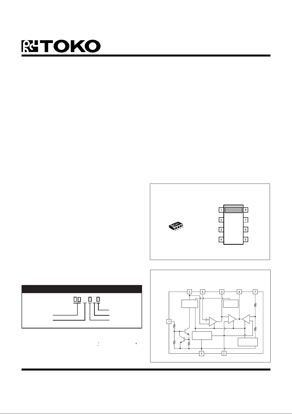
TK732xx
C
PULSE
CONTROL
GND
BASE
NOISE
BYPASS
V
SENSE
I
PK
V
IN
TK732xx
01S
FEATURES
■ Up to 5 A Output Current Capability With External
PNP Transistor
■ Internal Short Circuit Protection
■ Excellent Load Regulation
■ CMOS/TTL-Compatible On/Off Switch
■ Internal Reverse Bias Current Protection Switch
■ Internal Thermal Shutdown
■ Broad Operating Voltage Range
■ High Impedance V
SENSE
Pin (Off Mode)
■ Continuous and Pulsed Current Modes
APPLICATIONS
■ Battery Powered Systems
■ Cellular/Cordless Telephones
■ Radio Control Systems
■ Wireless Communications Systems
■ Portable Instrumentations
■ Portable Computers
■ Personal Digital Assistants
■ Local Area Network (LAN) Receivers
■ Lithium Ion Battery Chargers
■ Power Recovery for Microprocessors
VOLTAGE CODE
20 = 2.0 V * 32 = 3.2 V 44 = 4.4 V
21 = 2.1 V * 33 = 3.3 V 45 = 4.5 V
22 = 2.2 V * 34 = 3.4 V 46 = 4.6 V
23 = 2.3 V * 35 = 3.5 V 47 = 4.7 V
24 = 2.4 V 36 = 3.6 V 48 = 4.8 V
25 = 2.5 V 37 = 3.7 V 49 = 4.9 V
26 = 2.6 V 38 = 3.8 V 50 = 5.0 V
27 = 2.7 V 39 = 3.9 V 55 = 5.5 V *
28 = 2.8 V 40 = 4.0 V 70 = 7.0 V *
29 = 2.9 V 41 = 4.1 V 80 = 8.0 V
30 = 3.0 V 42 = 4.2 V 11 = 11.0 V
31 = 3.1 V 43 = 4.3 V
TK732 M L
ORDERING INFORMATION
Tape/Reel Code
TAPE/REEL CODE
L: Tape Left
TEMP. RANGE
C: -30 to 80 C **
I : -40 to 85
C
Temp. Code
Package Code
Voltage Code
Grade
* Unavailable with I Rank
** unless Otherwise Specified
*** TK73241MCLH, TK73242MCLH Available Only
PACKAGE CODE
M: SOT-23L-8
GRADE
None: Standard 2%
H: High (Special) **
*
BLOCK DIAGRAM
DESCRIPTION
The TK732xx is a controller IC for a low dropout voltage
regulator. The TK732xx and the external PNP power
transistor provide standard output voltages from 2 to 11 V
and output current from 100 mA to 5 A. By utilizing an
external PNP power transistor, low dropout voltage at high
current can be readily achieved. The internal electronic
switch can be controlled by TTL or CMOS logic levels. The
device is in the “on” state when the control pin is pulled to
a high logic level. A pin for a bypass capacitor, which
connects to the internal circuitry, is provided to lower the
overall output noise level.
The current limit characteristics can be configured as
continuous (constant current) or pulsed (cycling). An internal
thermal shutdown circuit limits the junction temperatures
to below 150 °C. In the “off” mode, the output of the
regulator becomes a high impedance. This prevents the
output capacitor from being rapidly discharged for backup
to the load.
CONTROL
NOISE BYPASS
V
IN
THERMAL
SENSOR
ON/OFF
CIRCUIT
BANDGAP
REFERENCE
LEAKAGE
PROTECTION
I
PK C
PULSE
BASEVSENSE
GND
LOW DROPOUT REGULATOR
Page 2
Page 2 January 1999 TOKO, Inc.
TK732xx
ABSOLUTE MAXIMUM RATINGS (STANDARD DEVICES) (NOTE 6)
Supply Voltage Range ............................................ 19 V
Power Dissipation (Note 1) ................................ 600 mW
Reverse Bias Voltage Range ..................................... 6 V
Noise Bypass Pin Terminal Voltage Range ............... 5 V
Control Pin Terminal Voltage Range........................ 14 V
Storage Temperature Range ................... -55 to +150 °C
Operating Temperature Range ...................-30 to +80 °C
Extended Temperature Range................... -40 to +85 °C
Operating Voltage Range............................ 1.8 to 14.0 V
Junction Temperature ........................................... 150 °C
Lead Soldering Temperature (10 s) ...................... 235 °C
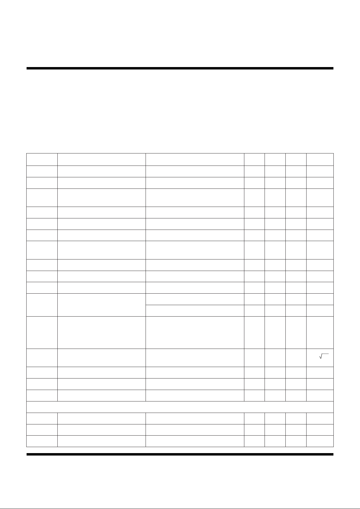
TK732xx ELECTRICAL CHARACTERISTICS (STANDARD DEVICES)
Test conditions: VIN = V
OUT(TYP)
+ 1 V, TA = 25 °C, unless otherwise specified.
LOBMYSRETEMARAPSNOITIDNOCTSETNIMPYTXAMSTINU
I
Q
tnerruCtnecseiuQI
TUO
IgnidulcxE,Am0=
TNOC
052063Aµ
I
YBTS
tnerruCybdnatSV
NI
FFOtuptuO,V8=1.0Aµ
I
)KAEL(R
)5etoN(egakaeLsaiBesreveR
V
R
lanretxEgnidulcxE,V5=
FFOtuptuO,rotsisnarT
205An
I
TUO
tnerruCtuptuOtnednepeDrotsisnarTlanretxEA/NA
V
TUO
egatloVtuptuOI
TUO
1elbaTeeS,Am03=V
V
PORD
egatloVtuoporDtnednepeDrotsisnarTlanretxEA/NV
geReniLnoitalugeReniL
VNIV=
)PYT(TUO
otV1+
V
)PYT(TUO
)2etoN(V6+
0.302Vm
gerdaoLnoitalugeRdaoLtnednepeDrotsisnarTlanretxE01Vm
I
)L(ESAB
WOLtnerruCesaBV8.1 ≤ VNI≤ V451Am
I
)H(ESAB
HGIHtnerruCesaBV1.4 ≤ VNI≤ V2104Am
V
ESNES
egatloVtceteDtimiLtnerruC
edoMtimiLtnerruCsuounitnoC08001021Vm
edoMtimiLtnerruCesluP0709011Vm
RRnoitcejeRelppiR
C,zH004=f
L
,Fµ01=
C
N
V,Fµ1.0=
NI
V=
)PYT(TUO
,V5.1=
I
TUO
V,Am03=
ELPPIR
,smrVm001=
)3etoN(
75Bd
V
ON
esioNtuptuO
,zHk03otzH004=FPB,zHk1=f
)3etoN(
31.0zH/Vµ
I
ESLUP
C
ESLUP
tnerruClanimreTniP)4etoN(515254Aµ
∆V
TUO
/∆T
tneiciffeoCerutarepmeT 02C°/mpp
V
fer
egatloVecnerefeR 52.1V
SNOITACIFICEPSLANIMRETLORTNOC
I
TNOC
tnerruClortnoCV
TNOC
NOtuptuO,V8.1=5.602Aµ
V
)NO(TNOC
)NO(egatloVlortnoCNOtuptuO8.1V
V
)FFO(TNOC
)FFO(egatloVlortnoCFFOtuptuO6.0V
Page 3
January 1999 TOKO, Inc. Page 3
TK732xx
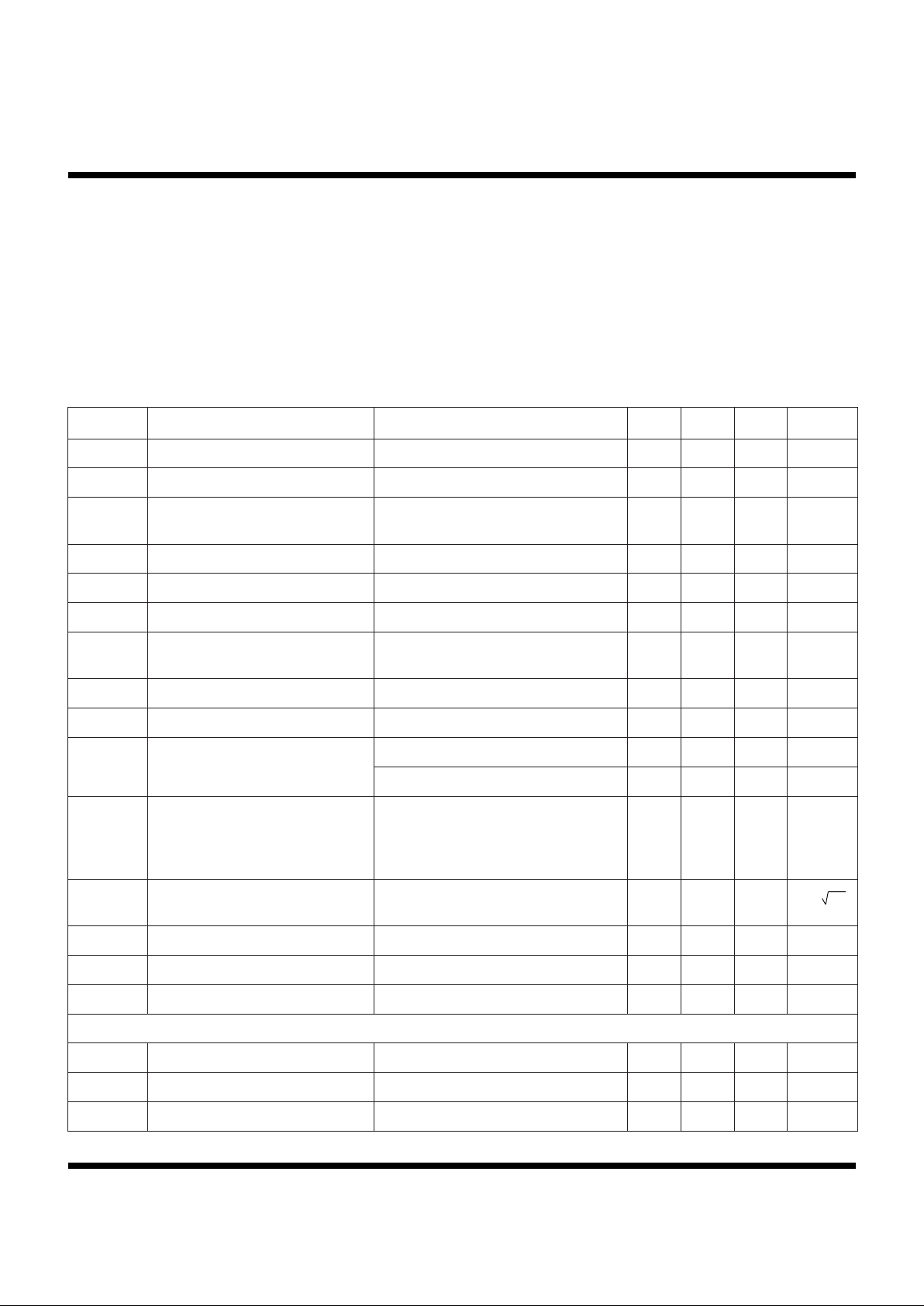
TK732xx ELECTRICAL CHARACTERISTICS TABLE 1 (STANDARD DEVICES)
Test Conditions: VIN = V
OUT(TYP)
+ 1 V, I
OUT
= 30 mA, TA = 25 °C, unless otherwise specified.
TK732xx ELECTRICAL CHARACTERISTICS (STANDARD DEVICES) CONT.
2.0 V 20 1.940 V 2.060 V
2.1 V 21 2.040 V 2.160 V
2.2 V 22 2.140 V 2.260 V
2.3 V 23 2.240 V 2.360 V
2.4 V 24 2.340 V 2.460 V 2.300 V 2.500 V
2.5 V 25 2.440 V 2.560 V 2.400 V 2.600 V
2.6 V 26 2.540 V 2.660 V 2.500 V 2.700 V
2.7 V 27 2.640 V 2.760 V 2.600 V 2.800 V
2.8 V 28 2.740 V 2.860 V 2.700 V 2.900 V
2.9 V 29 2.840 V 2.960 V 2.800 V 3.000 V
3.0 V 30 2.940 V 3.060 V 2.900 V 3.100 V
3.1 V 31 3.040 V 3.160 V 3.000 V 3.200 V
3.2 V 32 3.140 V 3.260 V 3.095 V 3.305 V
3.3 V 33 3.240 V 3.360 V 3.190 V 3.410 V
3.4 V 34 3.335 V 3.465 V 3.290 V 3.510 V
3.5 V 35 3.435 V 3.565 V 3.385 V 3.615 V
3.6 V 36 3.535 V 3.665 V 3.485 V 3.720 V
3.7 V 37 3.630 V 3.770 V 3.580 V 3.820 V
3.8 V 38 3.725 V 3.875 V 3.675 V 3.925 V
3.9 V 39 3.825 V 3.975 V 3.770 V 4.030 V
4.0 V 40 3.920 V 4.080 V 3.870 V 4.130 V
4.1 V 41 4.020 V 4.180 V 3.965 V 4.235 V
4.2 V 42 4.120 V 4.280 V 4.060 V 4.335 V
4.3 V 43 4.215 V 4.385 V 4.160 V 4.440 V
4.4 V 44 4.315 V 4.485 V 4.255 V 4.545 V
4.5 V 45 4.410 V 4.590 V 4.350 V 4.645 V
4.6 V 46 4.510 V 4.690 V 4.450 V 4.750 V
4.7 V 47 4.605 V 4.795 V 4.545 V 4.850 V
4.8 V 48 4.705 V 4.895 V 4.640 V 4.955 V
4.9 V 49 4.800 V 5.000 V 4.740 V 5.060 V
5.0 V 50 4.900 V 5.100 V 4.835 V 5.165 V
5.5 V 55 5.390 V 5.610 V
7.0 V 70 6.860 V 7.140 V
6.0 V 80 7.840 V 8.160 V 7.745 V 8.265 V
11.0 V 11 10.78 V 11.22 V 10.650 V 11.365 V
Note 1: Power dissipation is 600 mW when mounted as recommended. Derate at 4.8 mW/°C for operation above 25 °C.
Note 2: Refer to :Definition of Terms.”
Note 3: Ripple rejection and noise voltage are affected by the value and characteristics of the capacitor used.
Note 4: This pin is used for Pulse Current Limit Mode. When selecting Continuous Current Limit Mode, this pin is connected to GND.
Note 5: Not applicable for V
OUT
> 4.8 V.
Note 6: The voltage applied to any pin must be greater than -0.4 V.
Gen. Note: Parameters with min. or max. values are 100% tested at TA = 25 °C.
Room Temp. Range (TA = 25 °C) Full Temp. Range (TA = -40 to +85 °C)
(Applies to "I" Rank Only)
Output Voltage Voltage Code V
OUT(MIN)
V
OUT(MAX)
V
OUT(MIN)
V
OUT(MAX)
Page 4
Page 4 January 1999 TOKO, Inc.
TK732xx
ABSOLUTE MAXIMUM RATINGS (SPECIAL DEVICES) (Note 6)
Supply Voltage Range ............................................ 19 V
Power Dissipation (Note 1) ................................ 600 mW
Reverse Bias Voltage Range ..................................... 6 V
Noise Bypass Pin Terminal Voltage Range ............... 5 V
Control Pin Terminal Voltage Range........................ 14 V
Storage Temperature Range ................... -55 to +150 °C
Operating Temperature Range ...................-10 to +60 °C
Operating Voltage Range............................ 1.8 to 14.5 V
Junction Temperature ........................................... 150 °C
Lead Soldering Temperature (10 s) ...................... 235 °C
TK73241MCLH, TK73242MCLH ELECTRICAL CHARACTERISTICS
Test conditions: VIN = V
OUT(TYP)
+ 1 V, TA = 25 °C, unless otherwise specified.
LOBMYSRETEMARAPSNOITIDNOCTSETNIMPYTXAMSTINU
I
Q
tnerruCtnecseiuQI
TUO
IgnidulcxE,Am0=
TNOC
042003Aµ
I
YBTS
tnerruCybdnatSV
NI
FFOtuptuO,V8=1.0Aµ
I
)KAEL(R
)5etoN(egakaeLsaiBesreveR
V
R
lanretxEgnidulcxE,V5=
FFOtuptuO,rotsisnarT
205An
I
TUO
tnerruCtuptuOtnednepeDrotsisnarTlanretxEA/NA
V
TUO
egatloVtuptuOI
TUO
2elbaTeeS,Am03=V
V
PORD
egatloVtuoporDtnednepeDrotsisnarTlanretxEA/NV
geReniLnoitalugeReniL
V
NI
V=
)PYT(TUO
otV1+
V
)PYT(TUO
)2etoN(V6+
0.302Vm
gerdaoLnoitalugeRdaoLtnednepeDrotsisnarTlanretxE01Vm
I
ESAB
tnerruCesaB 05Am
V
ESNES
egatloVtceteDtimiLtnerruC
edoMtimiLtnerruCsuounitnoC58001511Vm
edoMtimiLtnerruCesluP5709501Vm
RRnoitcejeRelppiR
C,zH004=f
L
,Fµ01=
C
N
V,Fµ1.0=
NI
V=
)PYT(TUO
,V5.1=
I
TUO
V,Am03=
ELPPIR
,smrVm001=
)3etoN(
75Bd
V
ON
esioNtuptuO
,zHk03otzH004=FPB,zHk1=f
)3etoN(
31.0zH/Vµ
I
ESLUP
C
ESLUP
tnerruClanimreTniP)4etoN(515254Aµ
∆V
TUO
/∆T
tneiciffeoCerutarepmeT 02C°/mpp
V
fer
egatloVecnerefeR 52.1V
SNOITACIFICEPSLANIMRETLORTNOC
I
TNOC
tnerruClortnoCV
TNOC
NOtuptuO,V8.1=5.602A
V
)NO(TNOC
)NO(egatloVlortnoCNOtuptuO8.1V
V
)FFO(TNOC
)FFO(egatloVlortnoCFFOtuptuO6.0V
Page 5

January 1999 TOKO, Inc. Page 5
TK732xx
TK73241MCLH, TK73242MCLH ELECTRICAL CHARACTERISTICS CONT.
TK73241MCLH, TK73242MCLH ELECTRICAL CHARACTERISTICS TABLE 2
Test Conditions: VIN = V
OUT(TYP)
+ 1 V, I
OUT
= 30 mA, TA = 25 °C, unless otherwise specified.
Room Temp. Range (TA = 25 °C) Full Temp. Range (TA = -10 to +60 °C)
Output Voltage Voltage Code V
OUT(MIN)
V
OUT(MAX)
V
OUT(MIN)
V
OUT(MAX)
4.1 V 41 4.067 V 4.133 V 4.050 V 4.150 V
4.2 V 42 4.167 V 4.233 V 4.150 V 4.250 V
Note 1: Power dissipation is 600 mW when mounted as recommended. Derate at 4.8 mW/°C for operation above 25 °C.
Note 2: Refer to “Definition of Terms.”
Note 3: Ripple rejection and noise voltage are affected by the value and characteristics of the capacitor used.
Note 4: This pin is used for Pulse Current Limit Mode. When selecting Continuous Current Limit Mode, this pin is connected to GND.
Note 5: Not applicable for V
OUT
> 4.8 V.
Note 6: The voltage applied to any pin must be greater than -0.4 V.
Gen. Note: Parameters with min. or max. values are 100% tested at TA = 25 °C.
Page 6

Page 6 January 1999 TOKO, Inc.
TK732xx
CPC
N
V
IN
R
IPK
CONT
C
L
COLLECTOR
BASE
EMITTER
R
P
C
IN
V
OUT
TK732xx
EXTERNAL
TRANSISTOR
TYPICAL PERFORMANCE CHARACTERISTICS
TA = 25 °C, external transistor is 2SB1115(NEC), unless otherwise specified.
TEST CIRCUIT
V
OUT
(
5
0
m
V/
DIV)
LINE REGULATION 1
VIN (V)
0 10 20
V
OUT
(10
m
V/
DIV)
LINE REGULATION 2
VIN (V)
0 10 20
V
OUT
(
5 m
V/
DIV)
LOAD REGULATION
I
OUT
(mA)
0 500 1000
V
OUT
TYPICAL
I
Q
(
m
A)
3
5
QUIESCENT CURRENT
VS.
OUTPUT VOLTAGE
VIN (V)
1
0 10 20
4
2
0
V
OUT
= 3.0 V
V
OUT
= 5.0 V
V
DROP
(
m
V)
-200
0
DROPOUT VOLTAGE
VS.
OUTPUT VOLTAGE
I
OUT
(mA)
-400
0 500 1000
-100
-300
2SB799
2SB1115
2SB1114
2SB1302
I
GND
(
m
A)
3
5
GROUND CURRENT
VS.
OUTPUT VOLTAGE
I
OUT
(mA)
1
0 500 1000
4
2
0
Note:Transistor: 2SB1115
CN = 0.1 µF
CP = 0.1 µF
CL = 4.7 µF
RP = 330 k
Continuous Current Limit Mode:
I
SET
(mA) = 100 mV / R
IPK
(Ω)
Pulse Current Limit Mode:
I
SET
(mA) = 90 mV / R
IPK
(Ω)
Page 7

January 1999 TOKO, Inc. Page 7
TK732xx
∆
V
(
m
V)
100
CURRENT LIMIT DETECTOR VOLTAGE
VS. INPUT VOLTAGE
VIN (V)
50
0 5 10 15
CONTINUOUS CURRENT
LIMIT MODE
PULSE CURRENT
LIMIT MODE
I
B
(
m
A)
100
BASE CURRENT DRIVE
VS.
INPUT VOLTAGE
VIN (V)
50
0 5 10 15
I
REV
(A)
1E-6
REVERSE BIAS CURRENT
(VIN = 0 TO 6 V)
V
REV
(V)
1E-12
0 5 10
1E-9
VIN = 0 V
VIN = 6 V
VIN = 4 V
VIN = 2 V
I
Q
(A)
1E-6
QUIESCENT CURRENT
VS.
INPUT VOLTAGE (OFF MODE)
VIN (V)
1E-12
0 10 20
1E-9
RIPPLE REJECTION
0.01 0.1 1 10 100
f (kHz)
-80
RR (dB)
-20
-60
-40
0
-100
CN = 0.01 µF
CN = 0.1 µF
CN = NONE
I
CONT
(
µ
A)
50
CONTROL CURRENT
VS.
TEMPERATURE
TA (°C)
-50 0 50 100
20
40
30
10
0
V
CONT
= 5 V
V
CONT
= 2 V
V
OUT
(mV)
50
OUTPUT VOLTAGE VARIATION
VS.
TEMPERATURE
TA (°C)
-50 0 50 100
-10
30
10
-30
-50
V
OUT
TYPICAL
732xx
C
L
4.7 µF
V
OUT
V
IN
R
CONT
V
CONT
C
N
RIPPLE REJECTION CIRCUIT
V
CONT
(V)
2.0
CONTROL VOLTAGE (OUTPUT ON
POINT) VS. TEMPERATURE
TA (°C)
-50 0 50 100
1.0
R
CONT
= 0 Ω
TYPICAL PERFORMANCE CHARACTERISTICS (CONT.)
TA = 25 °C, external transistor is 2SB1115(NEC), unless otherwise specified.
Page 8

Page 8 January 1999 TOKO, Inc.
TK732xx
V
CONT
(V)
50
CONTROL PIN VOLTAGE
VS
.
CONTROL CURRENT
I
CONT
(µA)
-50 0 50 100
20
40
30
10
0
R
CONT
= 0 k
R
CONT
= 200 k
V
OUT
R
CONT
= 100 k
V
OUT
ON/OFF STEP RESPONSE
TIME (µs)
0 10 20 30
CL = 4.7 µF
CN = NONE
ON/OFF CONTROL
V
OUT
(200
m
V/
DIV)
LOAD CURRENT STEP RESPONSE
TIME (µs)
0 5 10 15 20
I
OUT
= 0 TO 300 mA
CL = 4.7 µF
CL = 10 µF
CL = 47 OR 100 µF
CL = 22 µF
V
OUT
(20
m
V/
DIV)
LINE CURRENT STEP RESPONSE
TIME (µs)
C
N
= 0.1 µF
I
OUT
= 50 mA
C
N
= NONE
V
OUT
+ 2 V
V
OUT
+ 1 V
V
OUT
V
IN
RISE TIME (µs)
ON/OFF TRANSIENT
CN (µF)
100
5000
10
0.001 0.01 0.1 10
1000
CL = 100 µF
CL = 4.7 µF OR 10 µF
CL = 22 µF
CL = 4.7 µF
TYPICAL PERFORMANCE CHARACTERISTICS (CONT.)
TA = 25 °C, external transistor is 2SB1115(NEC), unless otherwise specified.
Page 9

January 1999 TOKO, Inc. Page 9
TK732xx
DEFINITION AND EXPLANATION OF TECHNICAL TERMS
OUTPUT VOLTAGE (V
OUT
)
The output voltage is specified with VIN = (V
OUT(TYP)
+ 1 V)
and I
OUT
= 30 mA.
DROPOUT VOLTAGE (V
DROP
)
The dropout voltage is the difference between the input
voltage and the output voltage at which point the regulator
starts to fall out of regulation. Below this value, the output
voltage will fall as the input voltage is reduced. It is
dependent upon the load current, the external transistor
and the junction temperature.
BASE CONTROL CURRENT (I
BASE
)
The base control current is the drive current for the base of
the external transistor.
OUTPUT CURRENT (I
OUT
)
The output current depends on the characteristics of the
external transistor and current limit setting.
LINE REGULATION (Line Reg)
Line regulation is the ability of the regulator to maintain a
constant output voltage as the input voltage changes. The
line regulation is specified as the input voltage is changed
from VIN = V
OUT(TYP)
+ 1 V to VIN = V
OUT(TYP)
+ 6 V.
LOAD REGULATION (Load Reg)
Load regulation is the ability of the regulator to maintain a
constant output voltage as the load current changes. It is
a pulsed measurement to minimize temperature effects.
Load regulation depends on the external transistor.
QUIESCENT CURRENT (IQ)
The quiescent current is the current which flows through
the ground terminal under no load conditions (I
OUT
= 0 mA)
and excludes the control pin current.
GROUND CURRENT (I
GND
)
Ground current is the current which flows through the
ground pin(s). It is defined as I
IN
- I
OUT
, excluding control
current.
RIPPLE REJECTION RATIO (RR)
Ripple rejection is the ability of the regulator to attenuate
the ripple content of the input voltage at the output. It is
specified with 100 mVrms, 400 Hz superimposed on the
input voltage, where VIN = V
OUT(TYP)
+ 1.5 V. The output
decoupling capacitor is set to 10 µF, the noise bypass
capacitor is set to 0.1 µF, and the load current is set to
30 mA. Ripple rejection is the ratio of the ripple content of
the output vs. the input and is expressed in dB.
STANDBY CURRENT (I
STBY
)
Standby current is the current which flows into the regulator
when the output is turned off by the control function
(V
CONT
= 0 V). It is measured with VIN = 8 V (9 V for the
8 V output device).
REMOTE SENSING (V
SENSE
)
The V
SENSE
pin is the output voltage sensing pin. If the
voltage drop to the load caused by the PCB etch resistance
cannot be disregarded, the voltage drop can be
compensated by connecting the V
SENSE
pin as shown
below.
The length of the V
SENSE
etch should be limited to 30 cm
(11.8 in.) maximum.
COLLECTOR
V
OUT
EMITTER BASE
R
IPK
C
L
EXTERNAL
TRANSISTOR
TK732XX
Page 10

Page 10 January 1999 TOKO, Inc.
TK732xx
deliberately increase the output current (or raise the input
voltage) until the thermal protection circuit is activated.
Calculate the power dissipation of the device by subtracting
the output power from the input power. These
measurements should allow for the ambient temperature
of the PCB. The value obtained from PD /(150 °C - TA) is the
derating factor. The PCB mounting pad should provide
maximum thermal conductivity in order to maintain low
device temperatures. As a general rule, the lower the
temperature, the better the reliability of the device. The
thermal resistance when mounted is expressed as follows:
Tj = 0jA x PD + T
A
For Toko ICs, the internal limit for junction temperature is
150 °C. If the ambient temperature (TA) is 25 °C, then:
150 °C = 0jA x PD + 25 °C
0jA = 125 °C / P
D
PD is the value when the thermal sensor is activated. A
simple way to determine PD is to calculate VIN x IIN when
the output side is shorted. Input current gradually falls as
temperature rises. You should use the value when thermal
equilibrium is reached.
The range of usable currents can also be found from the
graph below.
Procedure:
1) Find P
D
2) PD1 is taken to be PD x (Note: It is not necessary to connect
a ceramic capacitor in parallel with an aluminum or tantalum output
capacitor. (~0.8 - 0.9)
SENSOR CIRCUITS
Overcurrent Sensor
The overcurrent sensor protects the device if the output is
shorted to ground.
Thermal Sensor
The thermal sensor protects the device if the junction
temperature exceeds the safe value (Tj = 150 °C). This
temperature rise can be caused by extreme heat, excessive
power dissipation caused by large output voltage drops, or
excessive output current. The regulator will shut off when
the temperature exceeds the safe value. As the junction
temperature decreases, the regulator will begin to operate
again. Under sustained fault conditions, the regulator
output will oscillate as the device turns off then resets.
Damage may occur to the device under extreme fault
conditions.
Reverse Voltage Protection
Reverse voltage protection prevents damage due to the
output voltage being higher than the input voltage. This
fault condition can occur when the output capacitor remains
charged and the input is reduced to zero, or when an
external voltage higher than the input voltage is applied to
the output side.
PACKAGE POWER DISSIPATION (PD)
This is the power dissipation level at which the thermal
sensor is activated. The IC contains an internal thermal
sensor which monitors the junction temperature. When the
junction temperature exceeds the monitor threshold of
150 °C, the IC is shut down. The junction temperature
rises as the difference between the input power (VIN x IIN)
and the output power (V
OUT
x I
OUT
) increases. The rate of
temperature rise is greatly affected by the mounting pad
configuration on the PCB, the board material, and the
ambient temperature. When the IC mounting has good
thermal conductivity, the junction temperature will be low
even if the power dissipation is great. When mounted on
the recommended mounting pad, the power dissipation of
the SOT-23L-8 is increased to 600 mW. For operation at
ambient temperatures over 25 °C, the power dissipation of
the SOT-23L-8 device should be derated at 4.8 mW/°C. To
determine the power dissipation for shutdown when
mounted, attach the device on the actual PCB and
DEFINITION AND EXPLANATION OF TECHNICAL TERMS (CONT.)
P
D
D
PD
25 50 75 150
(mW)
TA (°C)
3
6
5
4
Page 11

January 1999 TOKO, Inc. Page 11
TK732xx
3) Plot PD1 against 25 °C
4) Connect P
D1
to the point corresponding to the 150 °C
with a straight line.
5) In design, take a vertical line from the maximum
operating temperature (e.g., 75 °C) to the derating
curve.
6) Read off the value of PD against the point at which the
vertical line intersects the derating curve. This is taken
as the maximum power dissipation, DPD.
The maximum operating current is:
I
OUT
= (D
PD
/ (V
IN(MAX) - VOUT
)
SOT-23L-8 POWER DISSIPATION CURVE
V
IN
R
IPK
CONTROL
GND
GND
V
OUT
DEFINITIONS AND TERMS (CONT.)
0 50 100 150
TA (°C)
P
D
(mW)
0
450
750
150
300
600
MOUNTED AS
SHOWN
FREE AIR
INPUT-OUTPUT CAPACITORS
The output capacitor is necessary for stable operation.
The regulator may oscillate if the output capacitor is too
small or missing. The output capacitor size is determined
by load, transient response and external transistor used.
Evaluation in the circuit is recommended to ensure
performance requirements are satisfied. A minimum of 4.7
µF is necessary for stability, with twice that value
recommended. The minimum recommended input
capacitor is 1 µF. Problems do not occur with larger values
of capacitance. However, extremely low ESR may result in
unstable operation. Thus, the use of large value ceramic
capacitors is not recommended on the output.
BOARD LAYOUT
SOT-23L-8 BOARD LAYOUT
APPLICATION INFORMATION
Page 12

Page 12 January 1999 TOKO, Inc.
TK732xx
PULSE CURRENT LIMIT MODE
The equation for the pulse output current limit is as follows:
I
SET
(mA) = 90 (mV) / R
IPK
(Ω)
During the initial turn-on, charge (surge) current flows to
the output capacitor. This IC has a possibility for the
current limit to operate and to turn off the output by the
charge current of the output capacitor. Therefore, the
relationship between CL and CP is set as shown in the
graph below:
C
P
C
N
V
IN
COLLECTOR
BASE
EMITTER
R
P
330 k
V
OUT
V
CONT
C
L
R
IPK
C
IN
GND
EXTERNAL
TRANSISTOR
TK732xx
APPLICATION INFORMATION (CONT.)
C
L
(µF)
CP (µF)
100
1000
10
100.10.01
STABLE REGION
1
1
V
OUT
I
OUT
CONTINUOUS CURRENT LIMIT MODE
In the continuous current limit mode, the C
PULSE
pin (pin 3)
is directly connected to ground. The output current limit is
set by R
IPK
according to the following equation:
I
SET
(mA) = 100 (mV) / R
IPK
(Ω)
If the continuous current limit mode is also used for output
short circuit protection, the I
SET
value is set 50% to 100%
more than the maximum operating current. The current
transistor is selected from the I
SET
value. The output
voltage drops when the output current exceeds the I
SET
value. However, the output voltage returns to normal once
the output current decreases below the I
SET
value.
C
N
V
IN
COLLECTOR
BASE
EMITTER
V
OUT
V
CONT
C
L
C
IN
CONT
R
IPK
GND
EXTERNAL
TRANSISTOR
TK732xx
Page 13

January 1999 TOKO, Inc. Page 13
TK732xx
EXTERNAL PNP POWER TRANSISTOR
This IC can use any kind of external transistor. The external transistor selection is a function of the load current, Hfe and
power dissipation. See following chart:
HIGH-SIDE SWITCHING
High-side switching should not be implemented by an external transistor as shown above. This results in additional
voltage drop and loss of accuracy.
The high output voltage accuracy and low dropout voltage are maintained when the IC is turned ON/OFF by using the
control pin as illustrated above.
LOAD CURRENT RECOMMENDED EXTERNAL TRANSISTOR RECOMMENDED R
IPK
(Ω)
0 ~ 180 mA 2SB624, 2SB1115, 2SB799 (NEC), 2SB970 (Matushita) 0.33 ~ 0.39
0 ~ 300 mA 2SB1115, 2SB799 (NEC) 0.22 ~ 0.27
0 ~ 500 mA
2SB1114, 2SB1115 (NEC), 2SB1302 (Sanyo), 2SA1203,
2SA1213, 2SA1734 (Toshiba)
0.12 ~ 0.15
0 ~ 1 A 2SA1242, 2SA1736 (Toshiba), 2SB1302, 2SA1896 (Sanyo) 0.056 ~ 0.068
0 ~ 2 A 2SA1451, 2SA1242 (Toshiba) 0.033 ~ 0.039
0 ~ 3 A 2SA1451 (Toshiba), 2SA1645 (NEC) 0.022 ~ 0.027
0 ~ 4 A 2SA1451 (Toshiba), 2SB904 (Sanyo), 2SA1645 (NEC) 0.012 ~ 0.015
APPLICATION INFORMATION (CONT.)
ON/OFF
CONTROL
V
OUT
VOLTAGE
REGULATOR
V
DROP
TK732xx
V
OUT
V
IN
V
CONT
µ PRO
Page 14

Page 14 January 1999 TOKO, Inc.
TK732xx
VOLTAGE BACKUP OPERATION (HOLDUP TIME)
CL becomes the backup power supply when the
microprocessor is reset with the voltage detector IC
simultaneously with turning OFF the TK732xx. CL provides
the holdup time necessary to do an orderly shutdown of the
microprocessor.
PARALLEL ON/OFF CONTROL OPERATION
The figure above illustrates multiple regulators being
controlled by a single ON/OFF control signal. The series
resistor R is put in the input line of the low output voltage
regulator in order to prevent overdissipation. The voltage
dropped across the resistor reduces the large input-tooutput voltage across the regulator, reducing the power
dissipation in the device.
APPLICATION INFORMATION (CONT.)
OUTPUT VOLTAGE ADJUST
When a highly accurate output voltage is necessary, the
output can be adjusted. As shown above, higher output
resolution can be achieved by putting a resistor (R
ADJ
) in
the V
SENSE
pin in parallel with a 1000 pF capacitor. A value
of 2 K provides an adjustment of 50 mV typically. Note:
using this technique, the output voltage can only be
adjusted higher.
BATTERY CHARGER
Continuous Current Limit Mode:
I
SET
(mA) = 100 (mV) / R
IPK
(Ω)
732xx
V
OUT
V
IN
V
CONT
OFF
VOLTAGE
DETECTOR
IC
µ PRO
RESET
C
L
2 V
100 mA
TK732xx
5 V
5 A
V
IN
ON/OFF
CONTROL
3 V
100 mA
TK11230B
TK11220B
R
TK732xx
V
OUT
V
IN
V
CONT
V
SENSE
R
ADJ
1000 pF
V
CONT
V
IN
COLLECTOR
BASE
EMITTER
C
L
R
IPK
CONT
V
ADJ
LOAD
VOLTAGE DETECTOR
CIRCUIT
OR
MICROPROCESSOR
BATTERY
REMOTE
SENSING
CURRENT
LIMIT
SENSING
CONT
V
SENSE
V
OUT
EXTERNAL
TRANSISTOR
TK732XX
Page 15

January 1999 TOKO, Inc. Page 15
TK732xx
I
SET
(Continuous Current Limit Mode) is set to the desired
charging current.
LITHIUM ION BATTERY CHARGER WITH
OVERDISSIPATION PROTECTION OF EXTERNAL
TRANSISTOR (SHORT CIRCUIT MODE)
(RECOMMENDED WITH TK732xxMCLH)
During normal operation, Tr1 is turned ON, connecting pin
3 (C
PULSE
) to ground. This provides the continuous current
limit mode for normal operating conditions. During a short
CHARGING CHARACTERISTICS
I
OUT
FINISH CHARGE
SET CHARGING CURRENT
V
OUT
4.1 V
APPLICATION INFORMATION (CONT.)
V
IN
COLLECTOR
BASE
EMITTER
C
L
R
IPK
T
r1
LOAD
R
CONT
BATTERY
V
OUT
EXTERNAL
TRANSISTOR
TK732xx
circuit condition, Tr1 is turned “off.” This converts the circuit
into the pulse current limit mode of operation, reducing the
power dissipation in the pass transistor. The transition
between the continuous and pulse current limit modes can
be controlled by adjusting the operating point of Tr1 by the
value of resistor R.
Page 16

Page 16 January 1999 TOKO, Inc.
TK732xx
Marking Information
Product Code C
Voltage Code
TK73220 20
TK73221 21
TK73222 22
TK73223 23
TK73224 24
TK73225 25
TK73226 26
TK73227 27
TK73228 28
TK73229 29
TK73230 30
TK73231 31
TK73232 32
TK73233 33
TK73234 34
TK73235 35
TK73236 36
TK73237 37
TK73238 38
TK73239 39
TK73240 40
TK73241 41
TK73242 42
TK73243 43
TK73244 44
TK73245 45
TK73246 46
TK73247 47
TK73248 48
TK73249 49
TK73250 50
TK73255 55
TK73270 70
TK73280 80
TK73211 11
0.8
0.8
3.3
0.4
2.2
(0.3)
1.2
0.15
0.3
1.0
3.0
e
1
Recommended Mount Pad
5
1
0 - 0.1
15 max
e
4
e
8
0.1
Çl
0.1
0.45
1.4max
(3.4)
3.5
marking
Voltage Code
Product Code
Dimensions are shown in millimeters
Tolerance: x.x = ± 0.2 mm (unless otherwise specified)
+0.3
- 0.1
+0.15
- 0.15
+ 0.3
SOT-23L-8
PACKAGE OUTLINE
Printed in the USA
© 1999 Toko, Inc.
All Rights Reserved
TOKO AMERICA REGIONAL OFFICES
Toko America, Inc. Headquarters
1250 Feehanville Drive, Mount Prospect, Illinois 60056
Tel: (847) 297-0070 Fax: (847) 699-7864
IC-xxx-TK732xx
0798O0.0K
Visit our Internet site at http://www.tokoam.com
The information furnished by TOKO, Inc. is believed to be accurate and reliable. However, TOKO reserves the right to make changes or improvements in the design, specification or manufacture of its
products without further notice. TOKO does not assume any liability arising from the application or use of any product or circuit described herein, nor for any infringements of patents or other rights of
third parties which may result from the use of its products. No license is granted by implication or otherwise under any patent or patent rights of TOKO, Inc.
Western Regional Office
Toko America, Inc.
2480 North First Street , Suite 260
San Jose, CA 95131
Tel: (408) 432-8281
Fax: (408) 943-9790
Midwest Regional Office
Toko America, Inc.
1250 Feehanville Drive
Mount Prospect, IL 60056
Tel: (847) 297-0070
Fax: (847) 699-7864
Eastern Regional Office
Toko America, Inc.
107 Mill Plain Road
Danbury, CT 06811
Tel: (203) 748-6871
Fax: (203) 797-1223
Semiconductor Technical Support
Toko Design Center
4755 Forge Road
Colorado Springs, CO 80907
Tel: (719) 528-2200
Fax: (719) 528-2375
 Loading...