

Page 1
TISP5070H3BJ, TISP5080H3BJ, TISP5110H3BJ, TISP5150H3BJ
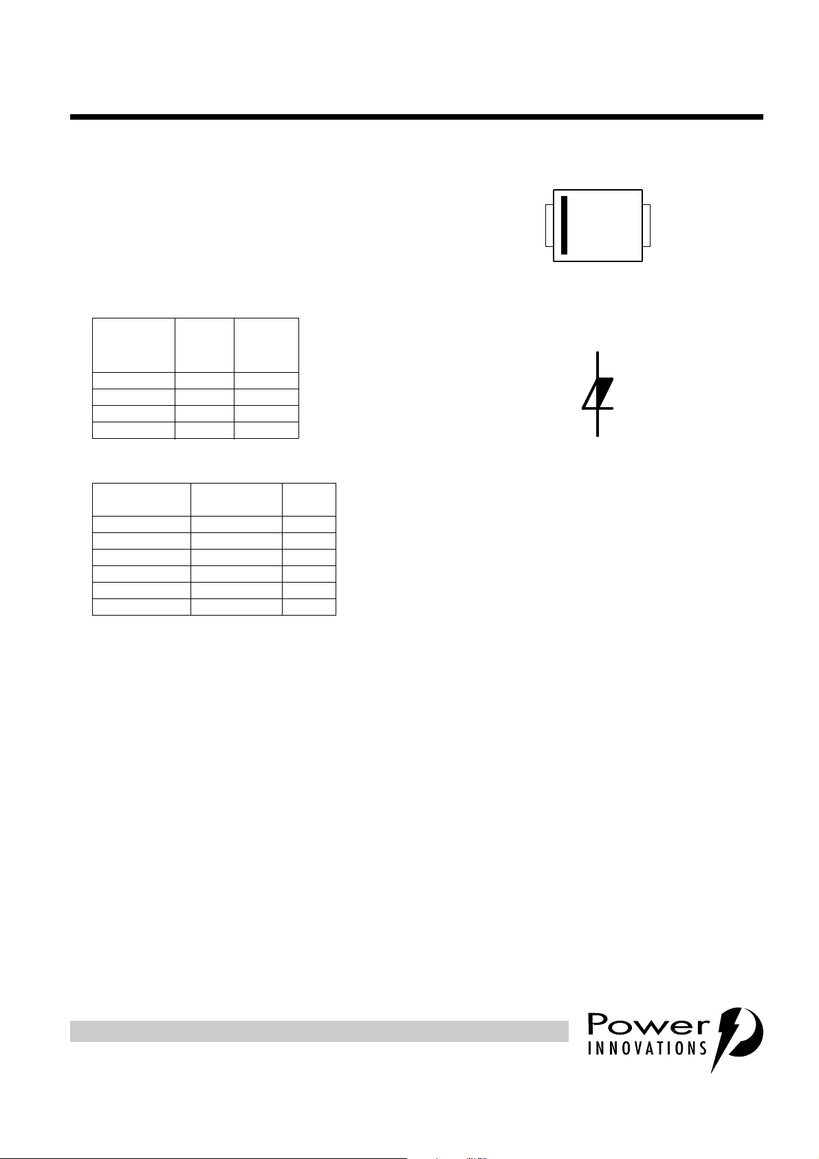
device symbol
SD5XAB
2
1
UNIDIRECTIONAL THYRISTOR OVERVOLTAGE PROTECTORS
TELECOMMUNICATION SYSTEM HIGH CURRENT OVERVOLTAGE PROTECTORS
●
Analogue Line Card and ISDN Protection
- Analogue SLIC
- ISDN U Interface
- ISDN Power Supply
●
8 kV 10/700, 200 A 5/310 ITU-T K20/21 rating
●
Ion-Implanted Breakdown Region
Precise and Stable Voltage
Low Voltage Overshoot under Surge
FORWARD-CONDUCTING
JANUARY 1998 - REVISED MARCH 1999Copyright © 1999, Power Innovations Limited, UK
SMBJ PACKAGE
(TOP VIEW)
12
MDXXBGB
V
DRM
DEVICE
‘5070 -58 -70
‘5080 -65 -80
‘5110 -80 -110
‘5150 -120 -150
●
Rated for International Surge Wave Shapes
WAVE SHAPE STANDARD
2/10 µs GR-1089-CORE 500
8/20 µs ANSI C62.41 300
10/160 µs FCC Par t 68 250
10/700 µs ITU-T K20/21 200
10/560 µs FCC Par t 68 160
10/1000 µs GR-1089-CORE 100
MINIMUM
V
V
(BO)
MAXIMUM
V
I
TSP
A
description
These devices are designed to limit overvoltages on the telephone and data lines. Overvoltages are normally
caused by a.c. power system or lightning flash disturbances which are induced or conducted on to the
telephone line. A single device provides 2-point protection and is typically used for the protection of ISDN
power supply feeds. Two devices, one for the Ring output and the other for the Tip output, will provide
protection for single supply analogue SLICs. A combination of three devices will give a low capacitance
protector network for the 3-point protection of ISDN lines.
PRODUCT INFORMATION
Information is current as of publication date. Products conform to speci fic ations in accordance
with the terms of Power Innovations standard warranty. Production processing does not
necessarily include testing of all parameters.
The protector consists of a voltage-triggered unidirectional thyristor with an anti-parallel diode. Negative
overvoltages are initially clipped by brea kdown clamping until the voltage r ises to the breakover level, which
causes the device to crowbar into a low-voltage on state. This low-voltage on state causes the current
resulting from the overvoltage to be safely diverted through the device. The high crowbar holding current
prevents d.c. latchup as the diver te d cu rrent s ubsides. Positive overvoltages are limi ted by the conduc tion o f
the anti-parallel diode.
This TISP5xxxH3BJ range consists of four voltage variants to meet vari ous maximum sys tem voltage levels
(58 V to 120 V). They are guaranteed to voltage limit and withstand the listed international lightning surges in
both polarities. The se hi gh (H ) c urre nt pr otecti on devices ar e in a pla stic pa ckage SMB J ( JEDE C DO- 21 4AA
with J-bend leads) and supplied in embossed carrier reel pack.
1
Page 2

TISP5070H3BJ, TISP5080H3BJ, TISP5110H3BJ, TISP5150H3BJ
FORWARD-CONDUCTING
UNIDIRECTIONAL THYRISTOR OVERVOLTAGE PROTECTORS
JANUARY 1998 - REVISED MA RCH 1999
T
absolute maximum ratings,
Repetitive peak off-state voltage, (see Note 1)
Non-repetitive peak on-state pulse current (see Notes 2, 3 and 4)
2/10 µs (GR-1089-CORE, 2/10 µs voltage wave shape) 500
8/20 µs (IEC 61000-4-5, 1.2/50 µs voltage, 8/20 current combination wave generator) 300
10/160 µs (FCC Part 68, 10/160 µs voltage wave shape) 250
5/200 µs (VDE 0433, 10/700 µs voltage wave shape) 220
0.2/310 µs (I3124, 0.5/700 µs voltage wave shape) 200
5/310 µs (ITU-T K20/21, 10/700 µs voltage wave shape) 200
5/310 µs (FTZ R12, 10/700 µs voltage wave shape) 200
10/560 µs (FCC Part 68, 10/560 µs voltage wave shape) 160
10/1000 µs (GR-1089-CORE, 10/1000 µs voltage wave shape) 100
Non-repetitive peak on-state current (see Notes 2, 3 and 5)
20 ms (50 Hz) full sine wave
16.7 ms (60 Hz) full sine wave
1000 s 50 Hz/60 Hz a.c.
Initial rate of rise of on-state current, Exponential current ramp, Maximum ramp value < 140 A di
Junction temperature T
Storage temperature range T
= 25°C (unless otherwise noted)
A
RATING SYMBOL VALUE UNIT
‘5070
‘5080
‘5110
‘5150
- 58
V
DRM
I
TSP
I
TSM
/dt 400 A/µs
T
J
stg
- 65
- 80
-120
55
60
2.1
-40 to +150 °C
-65 to +150 °C
V
A
A
NOTES: 1. See Figure 9 for voltage values at low er temperatures.
2. Initially the TISP5xxxH3BJ must be in thermal equilibrium with T
3. The surge may be repeated after the TISP5xxxH3BJ returns to its initial conditions.
4. See Figure 10 for current ratings at other temperatures.
5. EIA/JESD51-2 environment and EIA/JESD51-3 PCB with standard footprint dimensions connected with 5 A rated printed w iring
track widths. See Figure 8 for the current ratings at other durations. Derat e current v alues at -0.61%/°C for ambient temperatures
above 25 °C
=25°C.
J
electrical characteristics for terminal pair, TA = 25°C (unless otherwise noted)
PARAMETER TEST CONDITIONS MIN TYP MAX UNIT
I
DRM
V
V
I
(BO)
V
V
V
I
H
Repetitive peak offstate current
Breakover voltage dv/dt = -750 V/ms, R
(BO)
Impulse breakover
(BO)
voltage
Breakover current dv/dt = -750 V/ms, R
Forward voltage IF= 5 A, tW= 500 µs ‘5070 thru ‘5150 3 V
F
Peak forward recovery
FRM
voltage
On-state voltage IT=-5A, tW= 500 µs -3 V
T
Holding current IT= -5 A, di/dt = +30 mA/ms -0.15 -0.6 A
V
= V
D
DRM
Ω
= 300
SOURCE
dv/dt≥-1000 V/µs, Linear voltage ramp,
Maximum ramp value = -500 V
di/dt = -20 A/µs, Linear current ramp,
Maximum ramp value = -10 A
Ω
= 300
SOURCE
dv/dt≤+1000 V/µs, Linear voltage ramp,
Maximum ramp value = +500 V
di/dt = +20 A/µs, Linear current ramp,
Maximum ramp value = +10 A
TA = 25°C
T
= 85°C
A
‘5070
‘5080
‘5110
‘5150
‘5070
‘5080
‘5110
‘5150
-0.15 -0.6 A
‘5070 thru ‘5150 5 V
-5
-10
-70
-80
-110
-150
-80
-90
-120
-160
µA
V
V
PRODUCT INFORMATION
2
Page 3

TISP5070H3BJ, TISP5080H3BJ, TISP5110H3BJ, TISP5150H3BJ
FORWARD-CONDUCTING
UNIDIRECTIONAL THYRISTOR OVERVOLTAGE PROTECTORS
JANUARY 1998 - REVISED MARCH 1999
electrical characteristics for terminal pair, TA = 25°C (unless otherwise noted) (continued)
PARAMETER TEST CONDITIONS MIN TYP MAX UNIT
dv/dt
I
C
Critical rate of rise of
off-state voltage
Off-state current VD=-50V TA = 85°C -10 µA
D
Off-state capacitance
off
Linear voltage ramp, Maximum ramp value< 0.85V
f = 100 kHz, V
(see Note 6)
f = 100 kHz, V
f = 100 kHz, V
f = 100 kHz, V
= 1 Vrms, VD=-1V,
d
= 1 Vrms, VD=-2V
d
= 1 Vrms, VD=-50V
d
= 1 Vrms, VD= -100 V
d
DRM
‘5070
‘5080
‘5110
‘5150
‘5070
‘5080
‘5110
‘5150
‘5070
‘5080
‘5110
‘5150
‘5150
-5 kV/µs
300
280
240
140
260
245
205
120
90
80
65
35
30
420
390
335
195
365
345
285
170
125
110
90
50
40
pF
NOTE 6: Up to 10 MHz the capacitance is essentially independent of frequency. Above 10 MHz the effective capacitance is strongly
dependent on connection inductance.
thermal characteristics
PARAMETER
EIA/JESD51-3 PCB, I
= 25 °C, (see Note 7)
T
R
NOTE 7: EIA/JESD51-2 environment and PCB has standard footprint dimensions connected with 5 A rated printed wiring track widths.
Junction to free air thermal resistance
θ
JA
A
265 mm x 210 mm populated line card,
4-layer PCB, I
TEST CONDITIONS
= I
T
TSM(1000)
= I
T
TSM(1000)
, TA = 25 °C
,
MIN TYP MAX UNIT
113
°C/W
50
PRODUCT INFORMATION
3
Page 4
TISP5070H3BJ, TISP5080H3BJ, TISP5110H3BJ, TISP5150H3BJ
FORWARD-CONDUCTING
UNIDIRECTIONAL THYRISTOR OVERVOLTAGE PROTECTORS
JANUARY 1998 - REVISED MA RCH 1999
PARAMETER MEASUREMENT INFORMATION
+i
I
TSP
I
TSM
I
F
V
F
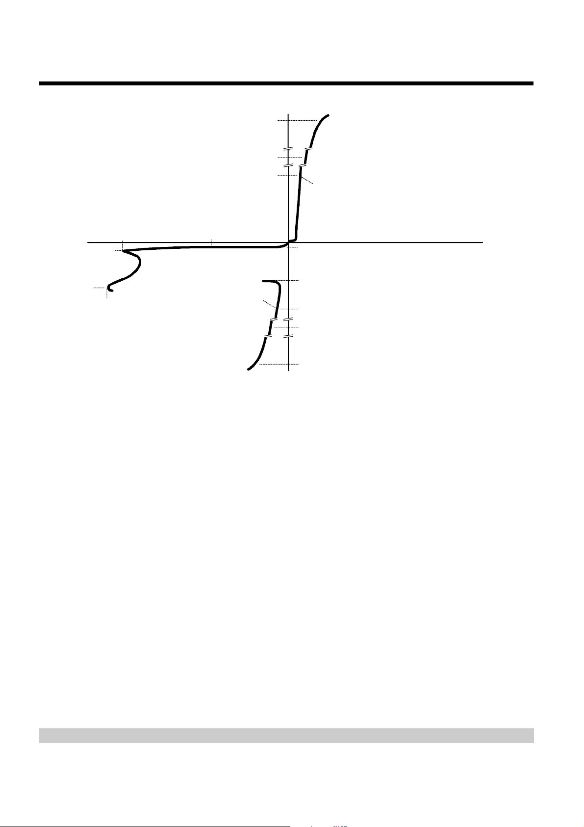
Quadrant I
Forward
Conduction
Characteristic
V
-v
I
(BO)
DRM
I
DRM
V
(BO)
Quadrant III
Switching
Characteristic
Figure 1. VOLTAGE-CURRENT CHARACTERISTIC FOR TERMINAL PAIR
V
D
I
D
I
H
V
T
I
T
I
TSM
I
TSP
-i
ALL MEASUREMENTS ARE REFERENCED TO TERMINAL 1
+v
PMXXACA
PRODUCT INFORMATION
4
Page 5
- Off-State Current - µA
NORMALISED BREAKO V ER VOLTAGE
vs
JUNCTION TEM P ERATURE
TJ - Junction Temperature - °C
-25 0 25 50 75 100 125 150
Normalised Breakover Voltage
0.95
1.00
1.05
1.10
TC5XAIA
NORMALISED HOLDING CURRENT
vs
JUNCTION T EM PERATURE
TJ - Junction Temperature - °C
-25 0 25 50 75 100 125 150
Normalised Holding Current
0.4
0.5
0.6
0.7
0.8
0.9
1.5
2.0
1.0
TC5XAD
D
I
100
10
0·1
0·01
TISP5070H3BJ, TISP5080H3BJ, TISP5110H3BJ, TISP5150H3BJ
FORWARD-CONDUCTING
UNIDIRECTIONAL THYRISTOR OVERVOLTAGE PROTECTORS
JANUARY 1998 - REVISED MARCH 1999
TYPICAL CHARACTERISTICS
OFF-ST AT E CURRE NT
vs
JUNCTION TEM P ERATURE
1
TC5XAFA
VD = -50 V
0·001
-25 0 25 50 75 100 125 150
T
- Junction Temperature - °C
Figure 2. Figure 3.
ON-STATE AND F ORWARD CURRENTS
vs
ON-STATE AND F ORWARD VOL TAGES
200
150
TA = 25 °C
100
t
= 100 µs
W
70
50
40
30
20
15
10
7
V
5
F
4
3
- On-State Curren t, Forward Current - A
F
2
, I
T
I
1.5
1
0.7 1.5 2 3 4 5 7110
TC5LAC
VT , VF- On-State Voltage, Forward Voltage - V
V
Figure 4. Figure 5.
T
PRODUCT INFORMATION
5
Page 6

TISP5070H3BJ, TISP5080H3BJ, TISP5110H3BJ, TISP5150H3BJ
E
FORWARD-CONDUCTING
UNIDIRECTIONAL THYRISTOR OVERVOLTAGE PROTECTORS
JANUARY 1998 - REVISED MA RCH 1999
TYPICAL CHARACTERISTICS
OFF-ST ATE CAPACITANCE
vs
OFF-STATE VOLTAGE
300
200
150
100
90
80
70
60
- Capacitance - pF
50
off
C
40
30
20
1 2 3 5 10 20 30 50 100
VD - Negative Off-state Voltage - V
TJ = 25°C
= 1 Vrms
V
d
Figure 6. Figure 7.
TC5XAB
'5070
'5080
'5110
'5150
DIFFERENTIAL OFF-STATE CAPACITANCE
vs
RATED REPETITIVE PEAK OFF-STATE VOLTAG
190
C - Differential Off-State Capacitance - pF
∆
∆∆
∆
180
170
160
150
140
130
120
110
100
90
80
'5070
'5080
58 65 80 120
V
- Negative Repetitive Peak Off-State Voltage - V
DRM
'5110
∆∆∆∆C = C
off(-2 V)
- C
TC5XAE
'5150
off(-50 V)
PRODUCT INFORMATION
6
Page 7

TISP5070H3BJ, TISP5080H3BJ, TISP5110H3BJ, TISP5150H3BJ
IMPULSE RATING
vs
AMBIENT T EM P ERATURE
TA - Ambient Temperature - °C
-40-30-20-100 1020304050607080
Impulse Current - A
80
90
100
120
150
200
250
300
400
500
600
700
IEC 1.2/50, 8/20
ITU-T 10/700
FCC 10/560
BELLCORE 2/10
BELLCORE 10/1000
FCC 10/160
TC5XAA
UNIDIRECTIONAL THYRISTOR OVERVOLTAGE PROTECTORS
RATING AND THERMAL INFORMATIO N
NON-REPETITIVE PEAK ON-ST AT E CURRENT
vs
30
20
15
10
CURRENT DURATION
V
= 600 Vrms, 50/60 Hz
GEN
GEN
/I
TSM(t)
= 1.4*V
R
GEN
EIA/JESD51-2 ENVIRONMENT
EIA/JESD51-3 PCB
= 25 °C
T
A
9
8
7
6
5
4
3
TI5HAC
FORWARD-CONDUCTING
JANUARY 1998 - REVISED MARCH 1999
- Non-Repetitive Peak On-State Current - A
2
TSM(t)
I
1.5
0·1 1 10 100 1000
t - Current Duration - s
Figure 8.
V
DERATING F ACTOR
DRM
vs
MINIMUM AM BI ENT TEMPERATURE
1.00
0.99
0.98
0.97
0.96
Derating Factor
0.95
0.94
0.93
PRODUCT INFORMATION
-35 -25 -15 -5 5 15 25-40 -30 -20 -10 0 10 20
T
- Minimum Ambient Temperature - °C
AMIN
Figure 9. Figure 10.
TI5XAD
7
Page 8

TISP5070H3BJ, TISP5080H3BJ, TISP5110H3BJ, TISP5150H3BJ
FORWARD-CONDUCTING
UNIDIRECTIONAL THYRISTOR OVERVOLTAGE PROTECTORS
JANUARY 1998 - REVISED MA RCH 1999
APPLICATIONS INFORMATION
deployment
These devices are two terminal overvoltage prote ctors. They may be used either singly to limi t the voltage
between two points (Figure 11) or in multiples to limit the voltage at several points in a circuit (Figure 12)
SIGNAL
AI4XAC
R1a
R1b
Figure 11. POWER SUPPLY PROTECTION
TISP5xxxH3BJ
-
D.C.
.
In Figure 11, the TISP5xxxH3B J limits the maximum voltage of the negati ve supply to -V
and +VF. This
(BO)
configuration can be used for protecting circuits where the voltage polarity does not reverse in normal
operation. In Figure 12, the two TISP5xxxH3BJ protectors, Th4 and Th5, lim it the maximum voltage of the
SLIC (Subscriber Line Interface Circuit) outputs to -V
and +VF. Ring and test protection is given by
(BO)
protectors Th1, Th2 and Th3. Pro tectors Th1 and Th2 limit the maximum tip and ri ng wire voltages to the
±V
of the individual protector. Protector Th3 limits the maximum voltage between the two conductors to its
(BO)
±V
value. If the equipment being protected has all its vulnerable components connected between the
(BO)
conductors and ground, then protector Th3 is not required.
TIP
WIRE
RING
WIRE
OVER-
CURRENT
PROTECTION
R1a
R1b
RING/TEST
PROTECTION
Th3
Th1
Th2
TEST
RELAY
S1a
S1b
S2b
RING
RELAY
S2a
SLIC
RELAY
S3a
S3b
SLIC
PROTECTION
TISP5xxxH3BJ
Th4
Th5
SLIC
V
BAT
TEST
EQUIP-
MENT
Figure 12. LINE CARD SLIC PROTECTION
PRODUCT INFORMATION
8
RING
GENERATOR
AI4XAA
Page 9

TISP5070H3BJ, TISP5080H3BJ, TISP5110H3BJ, TISP5150H3BJ
FORWARD-CONDUCTING
UNIDIRECTIONAL THYRISTOR OVERVOLTAGE PROTECTORS
JANUARY 1998 - REVISED MARCH 1999
broad-band protection.
The star-connection of th ree TISP5xxxH3 BJ protectors g ives a protection circui t which has a low differential
capacitance to ground (Figure 13). This example, a -100 V ISDN line is protect ed. In Figure 13, the ci rcuit
illustration A shows that protector Th1 will be forward biased as it is connected to the most negative potential.
The other two protectors, Th2 and Th3 will be reverse biased as protector Th1 will pull their common
connection to within 0.5 V of the negative voltage supply.
C
Th1
Th2
Th3
SIGNAL
0.5 V
600 pF
C
-99.5 V
29 pF
29 pF
C
-99.5 V
26 pF
26 pF
1 pF
A) STAR-CONNECTED
U-INTERFACE
PROTECTOR
- 100 V - 100 V - 100 V
B) EQUIVALENT
TISP5150H3BJ
CAPACITANCES
C) DELTA EQUIVALENT
SHOWS 25 pF
LINE UNBALANCE
AI4XAB
Figure 13. ISDN LOW CAPACITANCE U-INTERFACE PROTECTION
Illustration B shows the equivalent capacitances of the two reverse biased protectors (Th2 and Th3) as 29 pF
each and the capacitance of the forward biased protector (Th1) as 600 p F. Illustration C shows the delta
equivalent of the star capacitances of illustration B. The protector circuit differential capacitance will be 26 - 1
= 25 pF. In this circuit, th e differential capacita nce value cannot exceed the cap acitance value of the ground
protector (Th3).
A bridge circuit can be used for low capacitance differential. Whatever the potential of the ring and tip
conductors are in Figure 14, the array of steering diodes, D1 through to D6, ensure that terminal 1 of
protector Th1 is always positive with respect to terminal 2. The protection voltage will be the sum of the
protector Th1, V
, and the forward voltage of the appropr iate series diodes. It is important t o select the
(BO)
correct diodes. Diodes D3 through to D6 divert the currents from the ring and tip lines. Diodes D1 and D2 will
carry the sum of the ring and tip cu rrents and so conduct twice the current of the othe r four diodes. The
diodes need to be specified for forward recovery voltage, V
, under the expected impulse conditions.
FRM
(Some conventional a.c. rectifiers c an p roduc e a s muc h a s 70 V of forward recovery voltage, which would b e
an extra 140 V added to the V
of Th1). In principle the bridge circuit can be extended to protect more than
(BO)
two conductors by adding extra legs to the bridge.
RING
TIP
1
2
Th1
AI5XAC
Figure 14. LOW CAPACITANCE BRIDGE PROTECTION CIRCUIT
PRODUCT INFORMATION
D1D2D3D4D5
D6
9
Page 10

TISP5070H3BJ, TISP5080H3BJ, TISP5110H3BJ, TISP5150H3BJ
FORWARD-CONDUCTING
UNIDIRECTIONAL THYRISTOR OVERVOLTAGE PROTECTORS
JANUARY 1998 - REVISED MA RCH 1999
ISDN device selection
The ETSI Techn ical Report ETR 0 80:1993 d efines several range values in ter ms of maximum an d minimum
ISDN feeding voltages. The following table shows that ranges 1 and 2 can use a TISP5110H3BJ protector
and ranges 3 to 5 can use a TISP5150H3BJ protector.
FEEDING VOLTAGE STANDOFF VOLTAGE
RANGE
V
151 69
266 70
391 99
5 105 115
V
DRM
V
-80 TISP5110H3BJ
-120 TISP5150H3BJ4 90 110
impulse testing
To verify the withstand capabil ity and safety of the equipment , standards require that the equipm ent is test ed
with various impulse wave forms. The table below shows some common values.
DEVICE #MINIMUMVMAXIMUM
PEAK VOLTAGE
STANDARD
GR-1089-CORE
FCC Part 68
(March 1998)
I3124 1500 0.5/700 37.5 0.2/310 200 0
ITU-T K20/K21
† FCC Part 68 terminology for the waveforms produced by the ITU-T recommendation K21 10/700 impulse generator
SETTING
V
2500 2/10 500 2/10 500
1000 10/1000 100 10/1000 100
1500 10/160 200 10/160 250 0
800 10/560 100 10/560 160 0
1500 9/720 † 37.5 5/320 † 200 0
1000 9/720 † 25 5/320 † 200 0
1500
4000
VOLTAGE
WAVE FORM
µs
10/700
PEAK CURRENT
VALUE
A
37.5
100
CURRENT
WAVE FORM
µs
5/310 200 0
TISP5xxxH3
25 °C RATING
A
SERIES
RESISTANCE
Ω
0
If the impulse generator current exceeds the protectors current rating then a series resistance can be used to
reduce the curren t to the prot ectors rat ed value and so prevent possible failure. The required value of se rie s
resistance for a given waveform is given by the following calculations. First, the minimum total circuit
impedance is found by dividing the impulse generators peak voltage by the protectors rated current. The
impulse generators fictive impedance (generators pea k voltage divided by peak shor t circuit current) is then
subtracted from the m inimum total circ uit impe dance to give the requi red value of s eri es res istance. In so me
cases the equipme nt will require verifi cation over a temperature range. By usin g the rated waveform values
from Figure 10, the appropriate series resistor value can be calculated for ambient temperatures in the range
of -40 °C to 85 °C.
If the devices are used in a st ar-connectio n, then the ground r eturn pr otector, Th3 in Figure 13, will co nduct
the combined cu rre nt of p ro tec tors Th1 and Th2. Similarly in the br i dge c onn ect ion ( Fig ur e 1 4) , t he pr otec to r
Th1 must be rated for the sum of the conductor currents. In these cases, it may be necessary to include some
series resistance in the conductor feed to reduce the impulse current to within the protectors ratings.
a.c. power testing
The protector can withsta nd currents ap plied for times not exceeding tho se shown in Figu re 8. Current s that
exceed these times must be terminated or reduced to avoid protector failure. Fuses, PTC (Positive
Temperature Coefficient) resistors and fusible resistors are overcurrent protection devices which can be used
PRODUCT INFORMATION
10
Page 11

TISP5070H3BJ, TISP5080H3BJ, TISP5110H3BJ, TISP5150H3BJ
FORWARD-CONDUCTING
UNIDIRECTIONAL THYRISTOR OVERVOLTAGE PROTECTORS
JANUARY 1998 - REVISED MARCH 1999
to reduce the current fl ow. Pr otective fuses may range from a few hundred milliamperes to one ampere. In
some cases it may be necessar y to add some extra series res istance to prevent the fuse opening durin g
impulse testing. The current versus time cha racteristic of the overcurrent protector must be below the line
shown in Figure 8. In some ca ses there may be a further time limit imposed by the test standard ( e.g. UL
1459 wiring simulator failure).
capacitance
The protector characteristic off-state capacitance values are given for d.c. bias voltage, VD, values of -1 V,
-2 V and -50 V. The TISP5150H3BJ is also given for a bias of -100 V. Values for other voltages may be
determined from Figure 6. Up to 10 MHz the capacitance is essentially independent of frequency. Above
10 MHz the effective capacitance is s trongly dependent on connection inductan ce. In Figure 12, the typic al
conductor bias voltages will be about -2 V and -50 V. Figure 7 shows the differential (line unbalance)
capacitance caused by biasing one pr otector at -2 V and the other at -50 V. For example, the TISP5070H3BJ
has a differential capacitance value of 166 pF under these conditions.
normal system voltage levels
The protector should not clip or limit the voltages that occur in nor mal s ystem operatio n. Figure 9 al lows the
calculation of the protector V
than the maximum normal system volt ages. The TISP5150H3BJ, with a V
protect ISDN feed voltages having maximum values of -99 V, -110 V and -115 V (range 3 through to range 5).
These three range voltages represent 0.83 (99/120), 0.92 (110/120) and 0.96 (115/120) of the -120 V
TISP5150H3BJ V
-40 °C. Thus the supply feed voltages of -99 V (0.83) and -110 V ( 0.92) will not be c lipped at temperatures
down to -40 °C. The -115 V (0.96) feed supply may be clipped if the ambient temperature falls below -21 °C.
. Figure 9 shows that the V
DRM
value at temperatures below 25 °C. The calculated value should not be less
DRM
will have decreased to 0.944 of its 25 °C value at
DRM
of -120 V, can be used to
DRM
JESD51 thermal measurement method
To standardise thermal measurements, the EIA (Electronic Industries Alliance) has created the JESD51
standard. Part 2 of the standard (JESD51-2, 1995) describes the test environment. This is a 0.0283 m
cube which contains the test PCB (Printed Ci rcuit Board) horizontally mou nted at the centre. Part 3 of the
standard (JESD51-3, 199 6) defines two test PCB s for surface mount components; one for packages smaller
than 27 mm on a s ide and the othe r for packages up to 48 mm. The SMBJ measurements used the sm aller
76.2 mm x 114.3 mm (3. 0 “ x 4.5 “) PCB. The JESD51-3 PCBs are designed to have low effective thermal
conductivity (high th er mal resi stance) and represen t a worse case con dition . The PCBs us ed in the ma jority
of applications will a chieve lower values of thermal resis tance and s o can dis sipate higher power levels than
indicated by the JESD51 values.
3
(1 ft3)
PRODUCT INFORMATION
11
Page 12

TISP5070H3BJ, TISP5080H3BJ, TISP5110H3BJ, TISP5150H3BJ
FORWARD-CONDUCTING
UNIDIRECTIONAL THYRISTOR OVERVOLTAGE PROTECTORS
JANUARY 1998 - REVISED MA RCH 1999
MECHANICAL DATA
SMBJ (DO-214AA)
plastic surface mount diode package
This surface mount package consis ts of a ci rcuit mounted on a lead frame and e ncaps ulated within a plas tic
compound. The compound will withstand soldering temperature with no deformation, and circuit performance
characteristics will remain stable when operated in high humidity conditions. Leads require no additional
cleaning or processing when used in soldered assembly.
SMB
4,57
4,06
3,94
3,30
2,40
2,00
1,52
0,76
Index
Mark
(if needed)
2,10
1,90
5,59
5,21
2
0,20
0,10
2,32
1,96
ALL LINEAR DIMENSIONS IN MILLIMETERS
PRODUCT INFORMATION
12
MDXXBHA
Page 13

TISP5070H3BJ, TISP5080H3BJ, TISP5110H3BJ, TISP5150H3BJ
UNIDIRECTIONAL THYRISTOR OVERVOLTAGE PROTECTORS
recommended printed wiring footprint.
SMB Pad Size
2.40
ALL LINEAR DIMENSIONS IN MILLIMETERS
FORWARD-CONDUCTING
JANUARY 1998 - REVISED MARCH 1999
MECHANICAL DATA
2.54
2.16
MDXXBI
device symbolization code
Devices will be coded as below. Terminal 1 is identified by a bar index mark.
DEVICE
TISP5070H3BJ 5070H3
TISP5080H3BJ 5080H3
TISP5110H3BJ 5110H3
TISP5150H3BJ 5150H3
SYMOBLIZATION
CODE
carrier information
The carrier for production q uantities is embosse d tape reel p ack. Evaluation quanti ties will be shipped in the
most practical carrier.
CARRIER ORDER #
Embossed Tape Reel Pack
(3000 Devices are on a Reel)
TISP5xxxH3BJR
PRODUCT INFORMATION
13
Page 14

TISP5070H3BJ, TISP5080H3BJ, TISP5110H3BJ, TISP5150H3BJ
FORWARD-CONDUCTING
UNIDIRECTIONAL THYRISTOR OVERVOLTAGE PROTECTORS
JANUARY 1998 - REVISED MA RCH 1999
MECHANICAL DATA
tape dimensions
SMB Package Single-Sprocket Tape
8,10
7,90
Direction of Feed
4,10
3,90
2,05
1,95
ø 1,5 MIN.
Carrier Tape
Embossment
Index
Mark
1,65
1,55
20°
1,85
1,65
5,55
5,45
0 MIN.
Maximium com ponent
rotation
Typical compon ent
cavity centre line
Typical compon ent
centre line
0,40 MAX.
12,30
11,70
Cover
Tape
8,20
MAX.
4,5 MAX.
ALL LINEAR DIMENSIONS IN MILLIMETERS
NOTES: A. The clearance between the component and the cavity must be within 0,05 mm MIN. to 0,65 mm MAX. so that the
component cannot rotate more than 20° within the determined cavity.
B. Taped devices are supplied on a reel of the following dimensions:-
Reel diam et e r: 33 0 ±3 , 0 mm
Reel hub diameter 75 mm MIN.
Reel axial hole: 13,0 ±0,5 mm
C. 3000 devices are on a reel .
PRODUCT INFORMATION
14
MDXXBJ
Page 15

TISP5070H3BJ, TISP5080H3BJ, TISP5110H3BJ, TISP5150H3BJ
FORWARD-CONDUCTING
UNIDIRECTIONAL THYRISTOR OVERVOLTAGE PROTECTORS
JANUARY 1998 - REVISED MARCH 1999
IMPORTANT NOTICE
Power Innovations Limited (PI) reserves the right to make changes to its products or to discontinue any semiconductor product
or service without notice, and advises its customers to ver ify, before placing orders, that the information being relied on is
current.
PI warrants performance of its semiconductor products to the specifications applicable at the time of sale in accordance with
PI's standard w arr a nty. Testing and other quality contro l techniques are u til ized to the extent PI deems n ec es sa ry to suppo rt thi s
warranty. Specific testing of all parameters of each device is not necessarily performed, except those mandated by government
requirements.
PI assumes no liability for applications assistance, customer product design, software performance, or infringement of patents
or services described herein. Nor is any license, either express or implied, granted under any patent right, copyright, design
right, or other intellectual property right of PI covering or relating to any combination, machine, or process in which such
semiconductor products or services might be or are used.
PI SEMICONDUCTOR PRODUCTS ARE NOT DESIGNED, INTENDED, AUTHORISED, OR WARRANTED TO BE SUITABLE
FOR USE IN LIFE-SUPPORT APPLICATIONS, DEVICES OR SYSTEMS.
Copyright © 1999, Power Innovations Limited
PRODUCT INFORMATION
15
 Loading...