

Page 1
TDA4472-M
Video-IF and Quasi Parallel Sound Processing
Description
The TDA4472 is an integrated bipolar circuit for video/
sound IF (VIF/SIF) signal processing in TV/VCR and
multimedia applications. The circuit processes all TV
Features
D
5 V supply voltage; low power consumption
D
Active carrier generation by FPLL principle
(frequency-phase-locked-loop) for true
synchronous demodulation
D
Very linear video demodulation, good pulse response
and excellent intermodulation figures
D
VCO circuit operates at picture carrier frequency
D
Alignment-free AFC without external reference
circuit, polarity of the AFC curve is switchable
video IF signals with negative modulation (e.g., B/G
standard), and the FM/NICAM sound IF signals.
D
Alignment-free quasi parallel sound (QPS) mixer for
FM/NICAM sound IF signals
D
Intercarrier output signal is gain controlled (necessary
for digital sound processing)
D
Separate SIF-AGC with average detection
D
Two independent SIF inputs
D
Package and relevant pinning is compatible with the
multistandard version TDA4470, which simplifies the
design of an universal IF module
D
VIF-AGC with peak sync. detection
D
Tuner AGC with adjustable take over point
Package: SDIP28, SO28
Ordering Information
Extended Type Number Package Remarks
TDA4472-MSD SDIP28
TDA4472-MFLG3 SO28 Delivery in taped form
TELEFUNKEN Semiconductors
Rev . A2, 15-Oct-96
1 (14)
Preliminary Information
Page 2
TDA4472-M
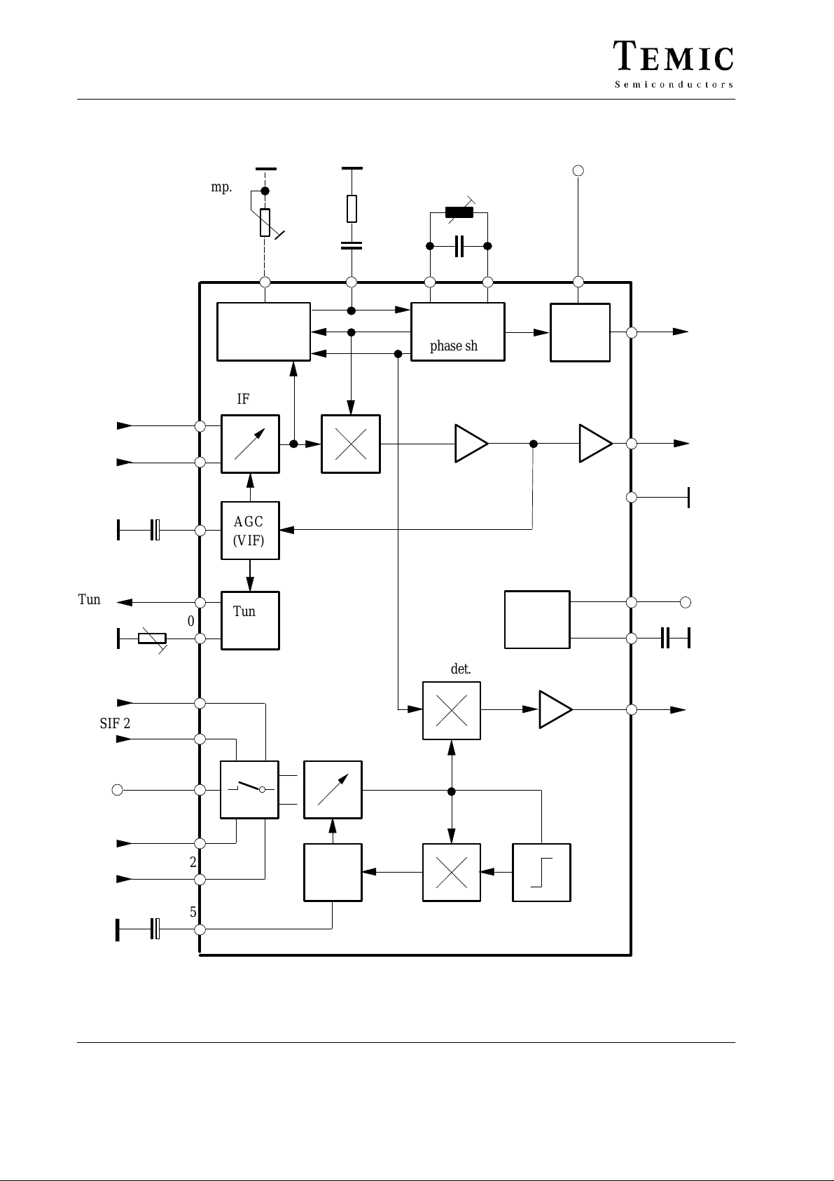
Block Diagram
VIF
C
AGC
Offset
comp.
(optional)
VIF amp
6
7
8
26
FPL
L
AGC
(VIF)
Loop
filter
Video
det.
18
0°
90°
VCO
2 0
phase shift
VCO
+
21
AFC
AFC
switch
19
22
12
4,9,16
AFC
Video
Tuner
Take over point
SIF 2
Input switch
SIF 1
C
AGC
11
10
27
28
23
Tuner
AGC
FM det.
SIF amp
3
1
2
5
AGC
(SIF)
Supply
17
C
24
(FM / NICAM)
94 8719
V
S
Ref
Intercarrier
2 (14)
Figure 1. Block diagram
TELEFUNKEN Semiconductors
Rev . A2, 15-Oct-96
Preliminary Information
Page 3

Circuit Description
Vision IF Amplifier
The video IF signal (VIF) is fed through a SAW filter to
the differential input (Pin 6-7) of the VIF amplifier. This
amplifier consists of three AC-coupled amplifier stages.
Each differential amplifier is gain controlled by the automatic gain control (VIF-AGC). The output signal of the
VIF amplifier is applied to the FPLL carrier generation
and the video demodulator.
Tuner-and VIF-AGC
At Pin 8, the VIF-AGC charges/discharges the AGC
capacitor to generate a control voltage for setting the gain
of the VIF amplifier and tuner in order to keep the video
output signal at a constant level. Therefore, in the case of
all negative modulated signals (e.g., B/G standard) the
sync. level of the demodulated video signal is the
criterion for a fast charge/discharge of the AGC capacitor .
The control voltage (AGC voltage at Pin 8) is transferred
to an internal control signal, and is fed to the tuner AGC
to generate the tuner AGC current at Pin 11 (open
collector output). The take over point of the tuner AGC
can be adjusted at Pin 10 by a potentiometer or an external
dc voltage (from interface circuit or microprocessor).
TDA4472-M
designed for low distortion and large bandwidth. The
demodulator output signal passes an integrated low pass
filter for attenuation of the residual vision carrier and is
fed to the video amplifier. The video amplifier is realized
by an operational amplifier with internal feedback and
8 MHz bandwidth (–3 dB). An additional noise clipping
is provided. The video signal is fed to VIF-AGC and to the
video output buffer . This amplifier with a 6 dB gain offers
easy adaption of the sound trap. For nominal video IF
modulation the video output signal at Pin 12 is 2 V
Sound IF Amplifier and SIF-AGC
The SIF amplifier is nearly identical with the 3-stage VIF
amplifier. Only the first amplifier stage exists twice and
is switchable by a control voltage at Pin 3. Therefore with
a minimal external expense it is possible to switch
between two different SAW filters. Both SIF inputs
features excellent cross-talk attenuation and an input
impedance which is independent from the switching
condition.
The SIF-AGC is related to the average level of FM-carrier
and controls the SIF amplifier to provide a constant SIF
signal to the QPS mixer.
pp.
FPLL, VCO and AFC
The FPLL circuit (frequency phase locked loop) consists
of a frequency and phase detector to generate the control
voltage for the VCO tuning. In the locked mode, the VCO
is controlled by the phase detector and in unlocked mode,
the frequency detector is superimposed. The VCO
operates with an external resonance circuit (L and C parallel) and is controlled by internal varicaps. The VCO
control voltage is also converted to a current and represents the AFC output signal at Pin 22.
A practicable VCO alignment of the external coil is the
adjustment to zero AFC output current at Pin 22. At center
frequency the AFC output current is equal to zero.
The optional potentiometer at Pin 26 allows an offset
compensation of the VCO phase for improved sound
quality (fine adjustment). Without a potentiometer (open
circuit at Pin 26), this offset compensation is not active.
The oscillator signal passes a phase shifter and supplies
the in-phase signal (0°) and the quadrature signal (90°)of
the generated picture carrier.
Video Demodulation and Amplifier
The video IF signal, which is applied from the gain
controlled IF amplifier, is multiplied with the inphase
component of the VCO signal. The video demodulator is
Quasi-Parallel-Sound (QPS) Mixer
The QPS mixer is realized by a multiplier. The SIF signal
(FM or NICAM carrier) is converted to the intercarrier
frequency by the regenerated picture carrier (quadrature
signal) which is provided from the VCO. The intercarrier
signal is fed via an output amplifier to Pin 24.
AFC Switch
The AFC output signal at Pin 22 can be controlled by a
switching voltage at Pin 19. It is possible to switch off the
AFC.
VCR Mode
For the VCR mode in a TV set (external video source
selected), it is recommendable to switch off the IF circuit.
With an external switching voltage at Pin 6 or 7, the IF
amplifiers are switched off and all signal output levels at
Pins 12 and 24 are according to the internal dc voltage.
Internal Voltage Stabilizer
The internal bandgap reference ensures constant performance independent of supply voltage and temperature.
TELEFUNKEN Semiconductors
Rev . A2, 15-Oct-96
3 (14)
Preliminary Information
Page 4
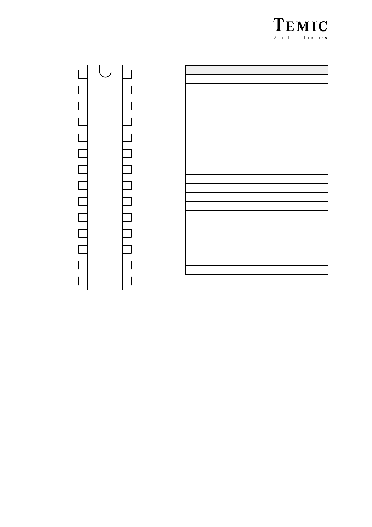
TDA4472-M
Pin Description
V
i,SIF1
V
i,SIF1
V
GND
C
V
i,VIF
V
i,VIF
C
GND
R
I
V
o,vid
NC
SW
AGC
AGC
top
tun
NC
1
2
3
4
5
6
7
8
9
10
11
12
13
14
94 8835
Figure 2. Pinning
28
27
26
25
24
23
22
21
20
19
18
17
16
15
V
i,SIF2
V
i,SIF2
R
comp
NC
V
o,FM
V
S
V
AFC
V
VCO
V
VCO
Vsw
LF
C
ref
GND
NC
Pin Symbol Function
1, 2 Vi,
3 V
SIF1 input (symmetrical)
SIF1
Input selector switch
sw
4, 9, 16 GND Ground
5 C
6, 7 V
8 C
10 R
11 I
12 V
AGC
i, VIF
AGC
top
tun
o,vid
SIF-AGC (time constant)
VIF input (symmetrical)
VIF-AGC (time constant)
Take over point, tuner AGC
Tuner AGC output current
Video output
13 NC Not connected
14 NC Not connected
15 NC Not connected
17 C
Internal reference voltage
ref
18 LF Loop filter
19 V
20, 21 V
22 V
23 V
24 VO,
VCO
AFC
AFC switch
sw
VCO circuit
AFC output
Supply voltage
S
Intercarrier output
FM
25 NC Not connected
26 R
27, 28 V
comp
i, SIF2
Offset compensation
SIF 2 input (symmetrical)
4 (14)
TELEFUNKEN Semiconductors
Rev . A2, 15-Oct-96
Preliminary Information
Page 5
Absolute Maximum Ratings
Reference point Pin 4 (9, 16), unless otherwise specified
Parameters Symbol Value Unit
Supply voltage Pin 23
SDIP28 package
SO28 package
Supply current Pin 23 I
Power dissipation SDIP28 package
SO28 package
Output currents Pins 12 and 24 I
External voltages
Pins 1, 2, 5 to 8, 10, 12, 17, 18 and 24, 26 to 28
Pins 20 and 21
Pin 11
Pins 3, 19 and 22
Junction temperature T
Storage temperature T
Electrostatic handling *) all pins V
*)
Equivalent to discharging a 200 pF capacitor trough a 0 W resistor.
V
V
V
S
S
s
P
P
out
ext
j
stg
ESD
TDA4472-M
9.0
6.0
93 mA
840
560
5 mA
+4.5
+3.5
+13.5
V
S
+125 °C
–25 to +125 °C
"
300
V
V
mW
mW
V
V
V
V
V
Operating Range
Parameters Symbol Value Unit
Supply voltage range Pin 23
SDIP28 package
SO28 package
Ambient temperature T
Thermal Resistance
Parameters Symbol Maximum Unit
Junction ambient, when soldered to PCB
SDIP28 package
SO28 package
R
R
V
V
amb
thJA
thJA
S
S
4.5 to 9.0
4.5 to 6.0
–10 to +85 °C
55
75
V
V
K/W
K/W
TELEFUNKEN Semiconductors
Rev . A2, 15-Oct-96
5 (14)
Preliminary Information
Page 6

TDA4472-M
Electrical Characteristics
VS = +5 V, T
= +25°C; reference point Pin 4 (9, 16), unless otherwise specified
amb
Parameters Test Conditions / Pins Symbol Min. Typ. Max. Unit
DC-supply Pin 23
Supply voltage – SDIP28
– SO28
Supply current I
V
S
V
S
S
4.5
4.5
5.0
5.0
9.0
5.5
V
V
85 93 mA
VIF-input Pin 6-7
Input sensitivity , (RMS value) For FPLL locked v
Input impedance See note 1 R
Input capacitance See note 1 C
in
in
in
80 120
m
1.2 k
2 pF
V
VIF-AGC Pins 8 and 15
IF gain control range G
AGC capacitor Pin 8 C
Black level capacitor Pin 15 C
Switching voltage: VCR mode See note 2 V
Switching current: VCR mode See note 2 I
v
AGC
BL
sw
sw
60 65 dB
2.2
m
100 nF
4.0 V
50
m
Tuner-AGC Pins 10 and 11 see note 3
A vailable tuner-AGC current I
Allowable output voltage V
IF slip – tuner AGC Current I
IF input signal for minimum
take over point
IF input signal for maximum
R
V)
R
top
top
: 10 to 90% ∆G
tun
= 10 kW (V
= 0, (V
top
= 0.8 V) v
top
= 4.5
v
tun
11
IF
in
in
1 2 4 mA
0.3 13.5 V
8 10 dB
4 mV
40 mV
take over point
Variation of the take over point
by temperature
∆T
= 55°C
amb
VIF-AGC: G
= 46 dB
v
∆v
in
2 3 dB
FPLL and VCO Pins 18, 20, 21 and 26 see note 4
Max. oscillator frequency For carrier generation f
Vision carrier capture range f
Oscillator drift (free running) as
function of temperature
= 38.9 MHz,
vco
C
= 8.2 pF
vco
See note 5,
∆Τ
= 55°C,
amb
C
= 8.2 pF,
vco
f
= 38.9 MHz
vco
∆f
∆f/
vco
cap
T
∆
70 MHz
±1.5 ±2 MHz
–0.3 %
Video output Pin 12
Output current – source
– sink
Output resistance See note 1 R
Video output signal Peak-to-peak value vo,
Difference of the video signals Between B/G and L ∆v
Sync. level V
Zero carrier level for neg.
modulation, ultra white level
Zero carrier level for pos.
modulation, ultra black level
V13 = V
V8 = 3 V
V13 = 0
V
= 3 V
8
S
Supply voltage influence on the
±I
sync
V
V
∆V/
12
out
vid
o,vid
DC
DC
V
5
2
3
100
mA
mA
W
1.8 2.0 2.2 Vpp
10 %
1.2 V
3.4 V
1.15 V
1 %/V
ultra white and ultra black level
Video bandwidth (–3 dB) RL ≥ 1 kW, CL ≤ 50 pF B 6 8 MHz
RMS
W
F
A
6 (14)
TELEFUNKEN Semiconductors
Rev . A2, 15-Oct-96
Preliminary Information
Page 7

TDA4472-M
UnitMax.Typ.Min.SymbolTest Conditions / PinsParameters
Video frequency response over
the AGC range
Differential gain error DG 2 5 %
Differential phase error DP 2 5 deg
Intermodulation
See note 6
1.07 MHz
Video signal to noise ratio W eighted, CCIR-567 S/
Residual vision carrier
fundamental wave 38.9 MHz
and second harmonic 77.8 MHz
Lower limiting level Below sync level ∆V
Upper limiting level Above ultra white level ∆V
Ripple rejection See note 1, Pin 23/Pin 12 RR 35 dB
AFC output Pin 22
Control slope ∆I/
Frequency drift by temperature Related to the picture
carrier frequency
Output voltage – upper limit
– lower limit
Output current I
AFC switch Pin 19
Control voltage: AFC “off”
AFC “on”
See note 7
Switching current I
SIF inputs Pin 1-2, 27-28
Input sensitivity
(RMS value)
Output signal
at Pin 24/25: –3 dB
Input impedance See note 1 R
Input capacitance See note 1 C
SIF-AGC Pin 5
IF gain control range G
AGC capacitor C
Intercarrier output-FM Pin 24 see note 8
DC output voltage V
Output resistance See note 1 R
Sound IF output voltage
vin = 10 mV v
(5.5 MHz output voltage)
Weighted signal to noise ratio:
(CCIR 468)
Ref. signal:
v
= 10 mV;
in
FM dev. = ±27 kHz
f
= 1 kHz;
mod
tested with the double
FM demod. U2860B;
B/G modulated VIF signal
Black screen: Channel 1/2
Grid pattern: Channel 1/2
Grey screen 50%: Channel
1/2
Ripple rejection See note 1, Pin 23/Pin 24 RR 35 dB
SIF input selector switch Pin 3
∆Β 2.0 dB
a
IM
N
v
res1
lim1
lim
f
∆
52 60 dB
56 60 dB
2 10 mV
400 mV
2
600 mV
0.7
m
0.25 0.6 %
V
AFC
VS–0.4
0.4
AFC
V
SW
v
AGC
S/N
S/N
S/N
SW
in
in
in
DC
out
out
0
3.5
v
60 65 dB
180 250 350 mV
±0.2 mA
0.8
V
S
±100
80 120
m
1.2 k
2 pF
10
2 V
150
60/58
54/52
60/57
A/kHz
V
V
V
V
m
A
V
RMS
W
m
W
RMS
dB
dB
dB
F
TELEFUNKEN Semiconductors
Rev . A2, 15-Oct-96
7 (14)
Preliminary Information
Page 8

TDA4472-M
Control voltage: – input 1 active
– input 2 active
Switching current I
Notes
1.)
This parameter is given as an application information and not tested during production.
2.)
In VCR mode the VIF- and SIF path is switched off.
3.)
Adjustment of turn over point (delayed tuner AGC) with external resistor R
4.)
Resonance circuit of VCO (fo = 38.9 MHz): C
Coil L
with unloaded Q-factor Qo w 60 for an oscillator voltage w 100 mV
VCO
(e.g. TOKO coil 7 KM, 292 XNS - 4051Z)
5.)
The oscillator drift is related to the picture carrier frequency, at external temperature-compensated LC circuit.
6.)
1.07) = 20 log (4.43 MHz component/1.07 MHz component); (1.07) value related to black-white signal
input signal conditions: picture carrier = 0 dB, colour carrier = –6 dB, sound carrier = –24 dB
7.)
Without control voltage at Pin 19 “AFC on” is automatically selected.
8.)
Picture carrier PC = 38.9 MHz; sound carrier SC1 = 33.4 MHz, SC
PC/SC
9.)
Without control voltage at Pin 3 the SIF input 1 is automatically selected.
=13 dB; PC/SC
1
SIF 2
Loop
comp.
See note 9 V
SW
2.0
0
SW
or external voltage V
= 8.2 – 10 pF,
VCO
= 20 dB; PC unmodulated (equivalent to sync. peak level).
2
Intercarrier
(FM/NICAM)
+V
AFC
S
2
top
= 33.16 MHz;
AFC
switch
Loop
filter
±100
at Pin 20 – 21
RMS
V
0.8
S
possible.
top
UnitMax.Typ.Min.SymbolTest Conditions / PinsParameters
V
V
A
L
VCO
10 k
NC NC
28 27 26 25 24 23 22 21 20 19
12
SIF 1
*) external L/C circuit (VCO 38.9 MHz)
with TOKO coil 7KM, 292XNS – 4051Z
354
SIF
Input switch
AGC (SIF)
6789
10 F 2.2 F
VIF
Figure 3. Test circuit
8.2 pF
AGC (VIF)
C
VCO
10 11 12 13 14
Tuner
delay
150
470 nF
18 17 16 15
10 k
Tuner
AGC
C
2.2 F
Video
Ref
94 9292
NCNC
8 (14)
TELEFUNKEN Semiconductors
Rev . A2, 15-Oct-96
Preliminary Information
Page 9

TDA4472-M
94 8721
AFC switch
AFC
+5 V
Intercarrier
(FM/NICAM)
S2
W
51 k
W
51 k
Loop
F
m
22 10 nF
Offset
filter
comp.
14
13
F
m
Ref
C
2.2
VCO
C
470 nF
NC NC
18 17 16 15
20 19
22 21
23
24
25
W
150
VCO
L
*)
8.2 pF
10 nF
W
10 k
NC NC
Video
W
10 k
Tuner
F
m
AGC (VIF)
VIF
6789101112
F
m
10 2.2
5
AGC (SIF)
34
S3
Input switch
2
Tuner
AGC
+12 V
*)
External L/C circuit (VCO: 38.9 MHz)
with TOKO coil 7KM, 292 XNS – 4051Z
SIF 2
28 27 26
SAW 2
10 nF
D/K
7
8
6
U4744B
2
1
10 nF
Figure 4. Basic application circuit
W
50
3
10 nF
in
IF
SIF 1
1
SAW 1
5
4
B/G
SAW: VIF
SAW driver
TELEFUNKEN Semiconductors
Rev . A2, 15-Oct-96
9 (14)
Preliminary Information
Page 10

TDA4472-M
Internal Pin Configuration
1, 27
2, 28
2 k
W
2 k
W
2 k
2 k
W
W
3 V
20 k
W
94 8521
Figure 5. Sound IF inputs (Pin 1-2, 27-28)
3.5 V
60 k
W
10 k
3
94 8522
Figure 6. Input selector switch (Pin 3)
W
2.3 V
4.2 V
94 8524
Figure 8. Video IF input (Pin 6-7)
94 8525
8
Figure 9. VIF-AGC time constant (Pin 8)
10 (14)
5
94 8523
Figure 7. SIF-AGC time constant (Pin 5)
Preliminary Information
3.5 V
6.5 k
W
6 k
W
94 8526
Figure 10. Tuner AGC – take over point (Pin 10)
TELEFUNKEN Semiconductors
Rev . A2, 15-Oct-96
Page 11

94 8527
TDA4472-M
Figure 11. Tuner AGC – output (Pin 11)
2.6 mA
94 8528
Figure 12. Video output (Pin 12)
2.75 V
Figure 14. Loop filter (Pin 18)
3.5 V
30 k
19
10.5 k
W
94 8533
Figure 15. AFC switch (Pin 19)
7 k
W
94 8532
W
7 k
W
3.5 V
Figure 13. Internal reference voltage (Pin 17)
TELEFUNKEN Semiconductors
Rev . A2, 15-Oct-96
94 8531
94 8534
Figure 16. VCO (Pin 20-21)
Preliminary Information
11 (14)
Page 12

TDA4472-M
94 8535
Figure 17. AFC output (Pin 22)
W
100
24
1 mA
94 8536
94 8538
10 k
Figure 19. VCO offset compensation (Pin 26)
3.5 V
10 k
W
W
Figure 18. Intercarrier output (Pin 24)
12 (14)
TELEFUNKEN Semiconductors
Rev . A2, 15-Oct-96
Preliminary Information
Page 13

Dimensions in mm
Package: SDIP28
TDA4472-M
95 10610
Package: SO28
95 10610
95 9932
TELEFUNKEN Semiconductors
Rev . A2, 15-Oct-96
13 (14)
Preliminary Information
Page 14

TDA4472-M
Ozone Depleting Substances Policy Statement
It is the policy of TEMIC TELEFUNKEN microelectronic GmbH to
1. Meet all present and future national and international statutory requirements.
2. Regularly and continuously improve the performance of our products, processes, distribution and operating systems
with respect to their impact on the health and safety of our employees and the public, as well as their impact on
the environment.
It is particular concern to control or eliminate releases of those substances into the atmosphere which are known as
ozone depleting substances (ODSs).
The Montreal Protocol ( 1987) and its London Amendments (1990) intend to severely restrict the use of ODSs and
forbid their use within the next ten years. Various national and international initiatives are pressing for an earlier ban
on these substances.
TEMIC TELEFUNKEN microelectronic GmbH semiconductor division has been able to use its policy of
continuous improvements to eliminate the use of ODSs listed in the following documents.
1. Annex A, B and list of transitional substances of the Montreal Protocol and the London Amendments respectively
2. Class I and II ozone depleting substances in the Clean Air Act Amendments of 1990 by the Environmental
Protection Agency (EPA) in the USA
3. Council Decision 88/540/EEC and 91/690/EEC Annex A, B and C (transitional substances) respectively.
TEMIC can certify that our semiconductors are not manufactured with ozone depleting substances and do not contain
such substances.
We reserve the right to make changes to improve technical design and may do so without further notice.
Parameters can vary in different applications. All operating parameters must be validated for each customer
application by the customer. Should the buyer use TEMIC products for any unintended or unauthorized
application, the buyer shall indemnify TEMIC against all claims, costs, damages, and expenses, arising out of,
directly or indirectly, any claim of personal damage, injury or death associated with such unintended or
unauthorized use.
14 (14)
TEMIC TELEFUNKEN microelectronic GmbH, P.O.B. 3535, D-74025 Heilbronn, Germany
Telephone: 49 (0)7131 67 2831, Fax number: 49 (0)7131 67 2423
TELEFUNKEN Semiconductors
Rev . A2, 15-Oct-96
Preliminary Information
 Loading...