

Page 1
Audioprocessor TDA 4390-2X
1 Overview
The TDA 4390-2X is a single-chip audio sound system.
The circuit can be partitioned into two functional
blocks.
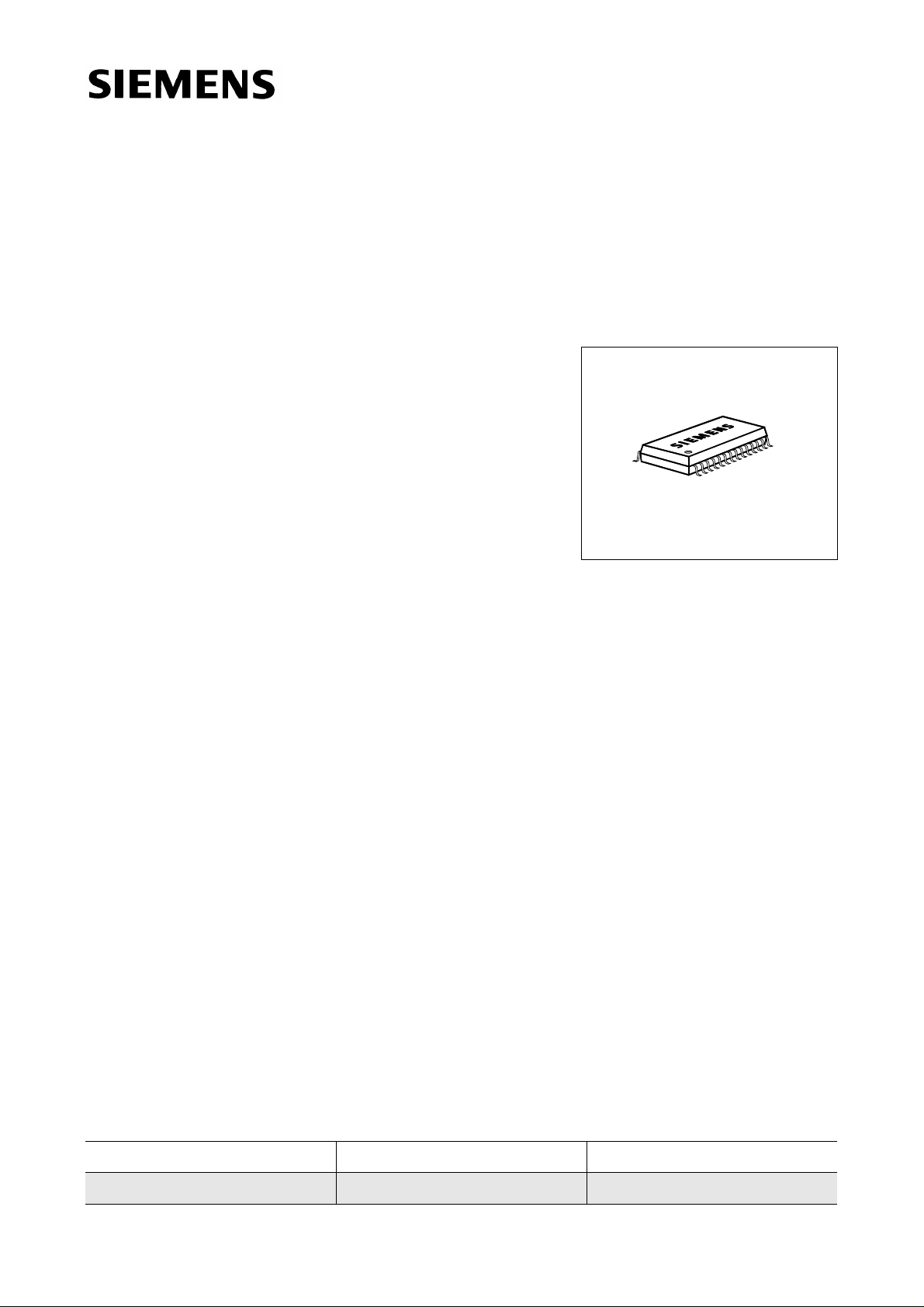
P-DSO-28-3
1.1 Features
1. Stereo sound processing
• Four stereo AF inputs
• Input/Output interface for external equalizer
• Max. gain switchable between 0 dB and 6 dB
• Bass and treble control
• Four independent attenuators for volume balance and fader control
2. Control part
2
• I
C Bus interface compatible for standard and fast mode
• Control of sound processing
Type Ordering Code Package
TDA 4390-2X Q67000-A5183 P-DSO-28-3
Semiconductor Group 1 02.96
Page 2
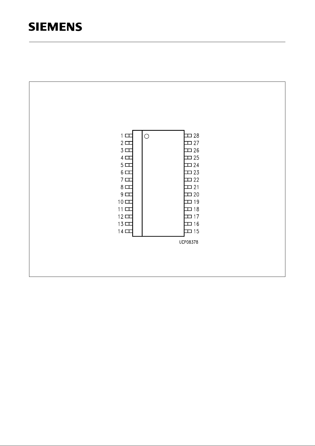
1.2 Pin Configuration
(top view)
TDA 4390-2X
P-DSO-28-3
Figure 1
Semiconductor Group 2 02.96
Page 3
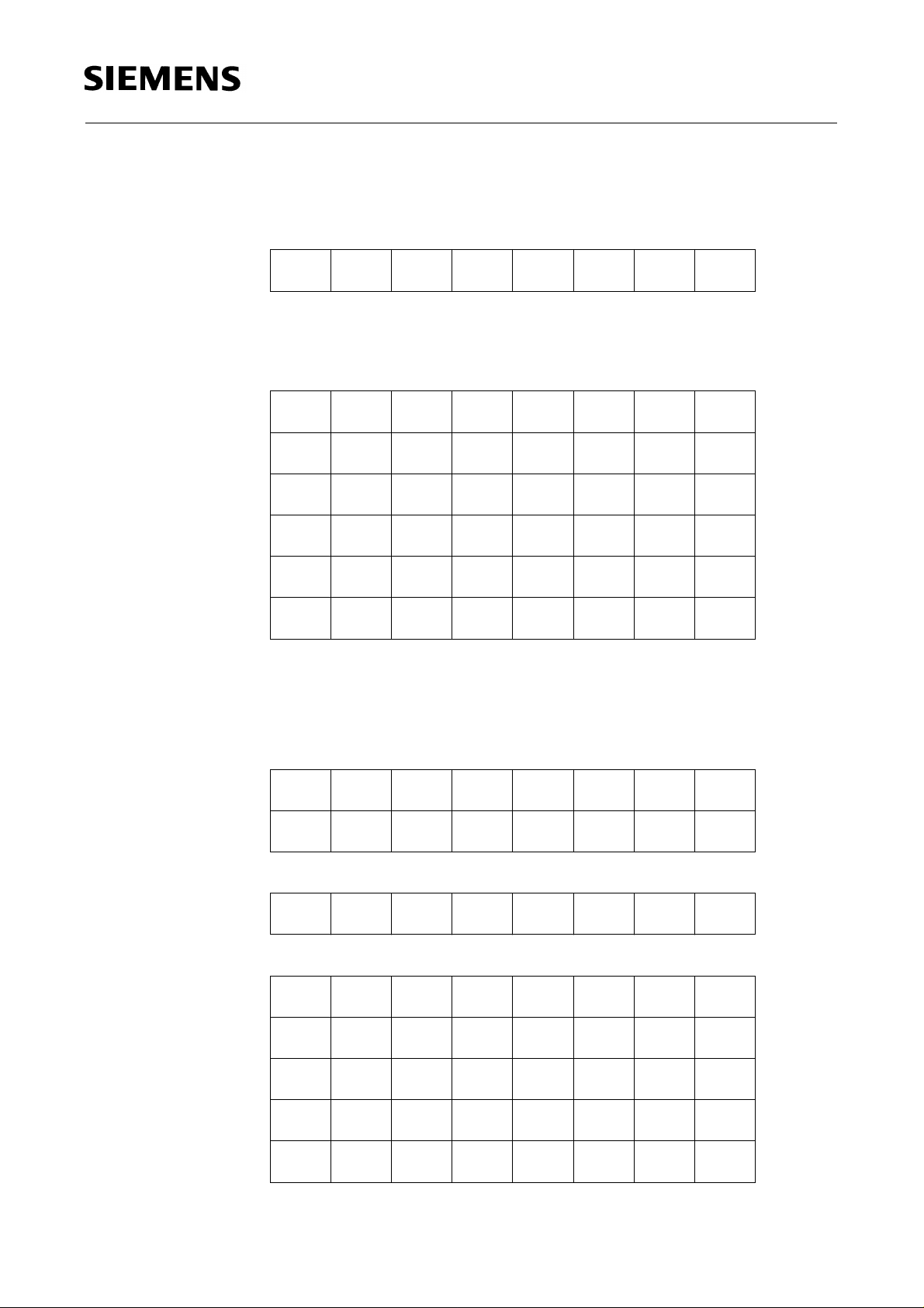
1.3 Pin Definitions and Functions
Pin No. Symbol Function
1 AF input 1 left
2 AF input 2 left
3 AF input 3 left
4 AF input 3 left
5 AF output switch left
6 AF input tone control volume left
7 Reset (all functions in power ON status)
8 I
9 I
2
C Bus SCL
2
C Bus SDA
TDA 4390-2X
10 Supply voltage
11 Corner frequency treble left
12 Corner frequency treble right
13 AF output right front
14 AF output right rear
15 AF output left rear
16 AF output left front
17 Corner frequency bass right output
18 Corner frequency bass right input
19 Corner frequency bass left output
20 Corner frequency bass left input
21 Ground
22 Blocking AF operating point
23 AF input tone control volume right
24 AF output switch right
25 AF input 4 right
26 AF input 3 right
27 AF input 2 right
28 AF input 1 right
Semiconductor Group 3 02.96
Page 4
1.3.1 Pin Description
TDA 4390-2X
Figure 2
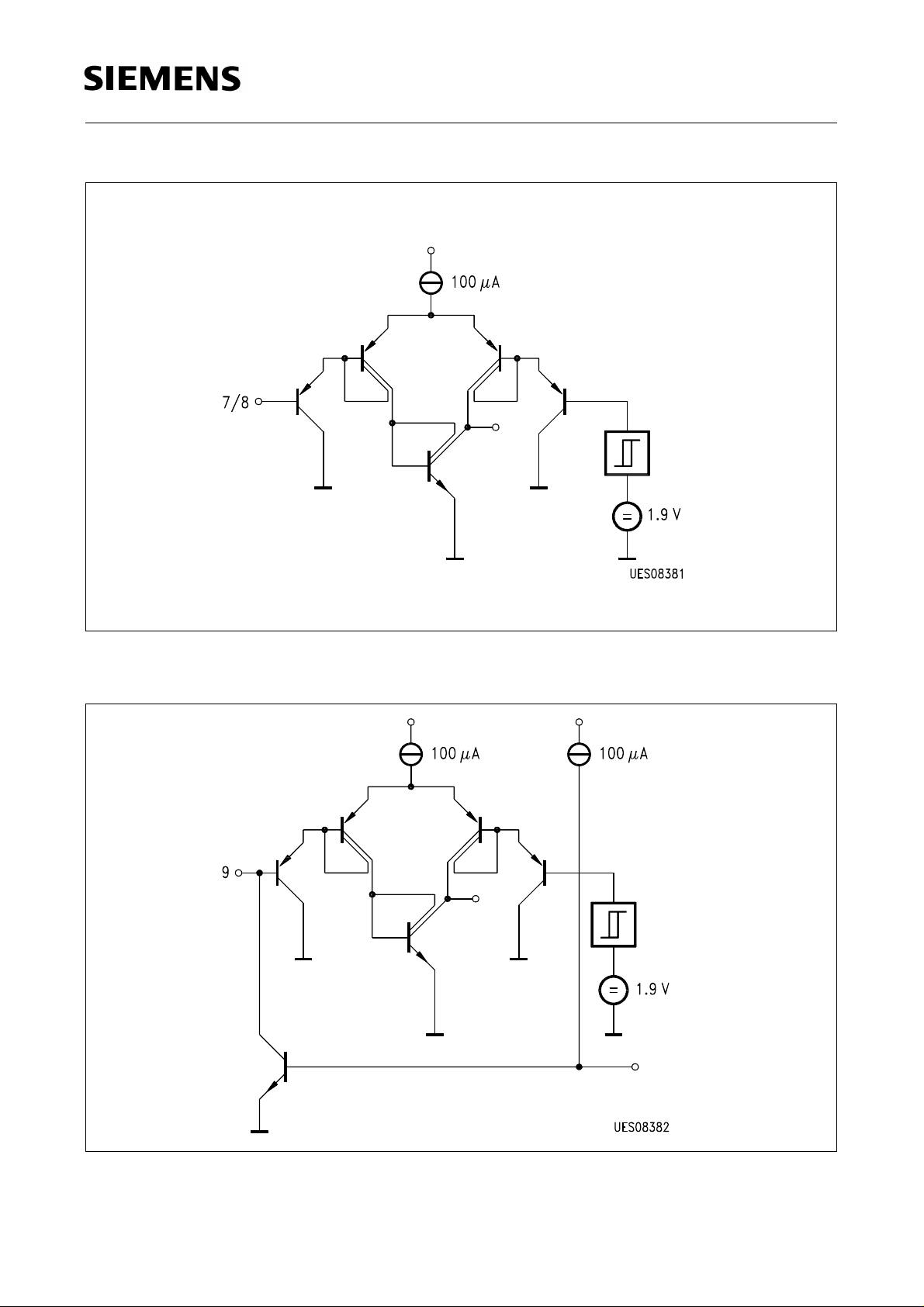
AF Inputs PIN 1/2/3/4/6/23/25/26/27/28
Figure 3
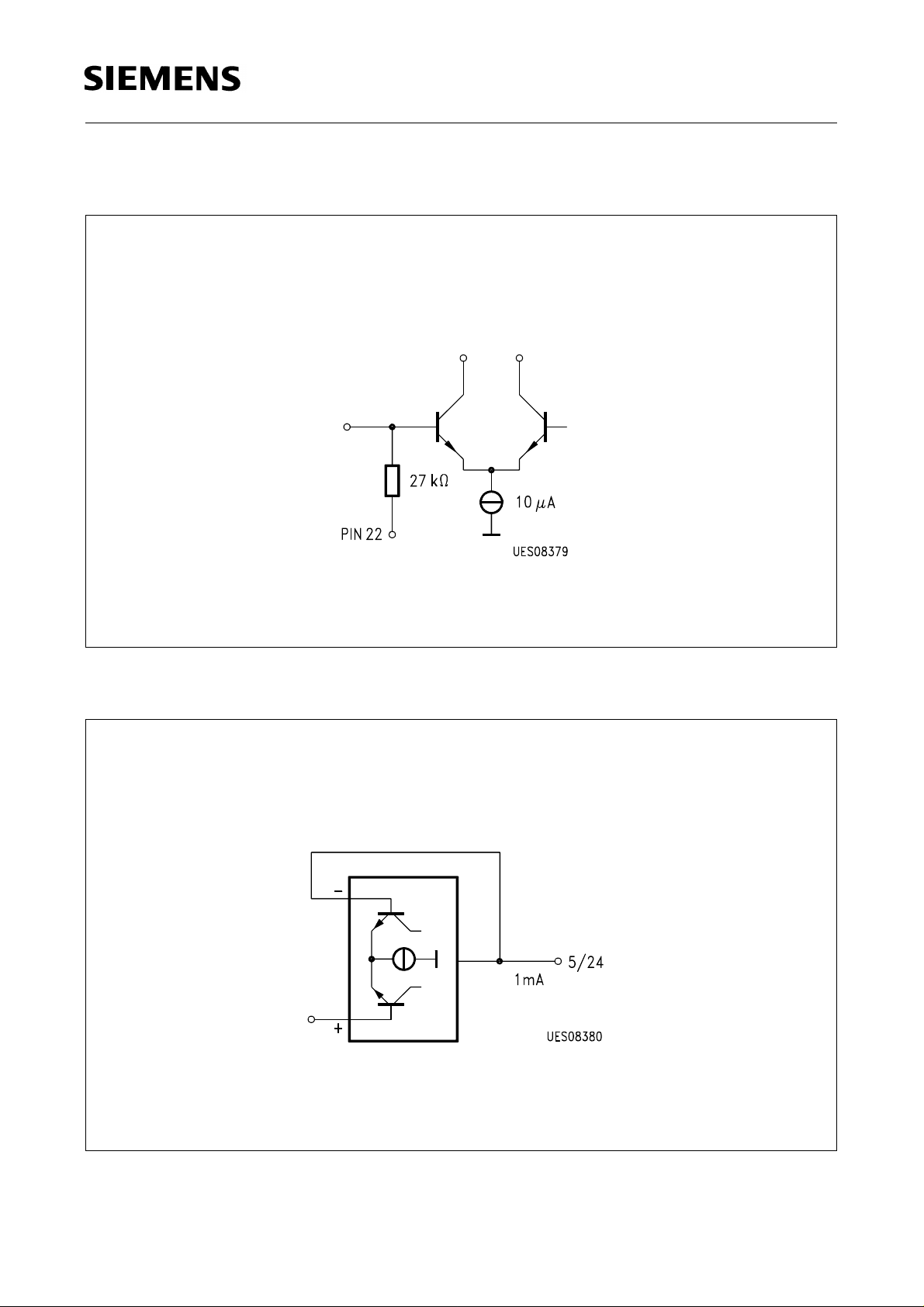
AF Outputs PIN 5/24
Semiconductor Group 4 02.96
Page 5
TDA 4390-2X
Figure 4
Reset PIN 7, I
2
C Bus SCL PIN 8
Figure 5
I2C Bus SDA PIN 9
Semiconductor Group 5 02.96
Page 6
TDA 4390-2X
Figure 6
Corner Frequency Treble PIN 11/12
Figure 7
AF Outputs PIN 13/14/15/16
Semiconductor Group 6 02.96
Page 7
TDA 4390-2X
Figure 8
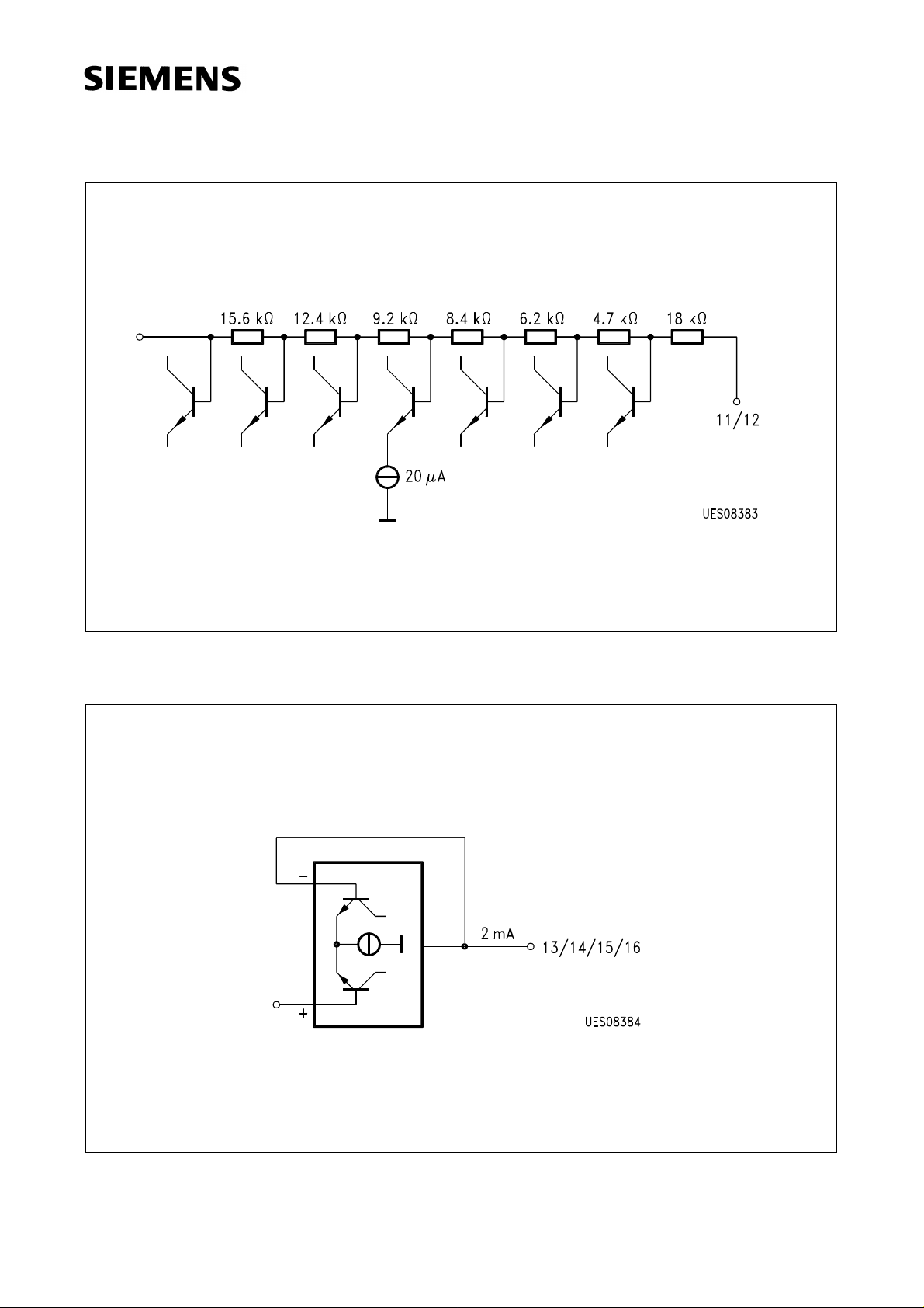
Corner Frequency Bass PIN 17/18/19/20
Figure 9
AF Operating Point PIN 22
Semiconductor Group 7 02.96
Page 8
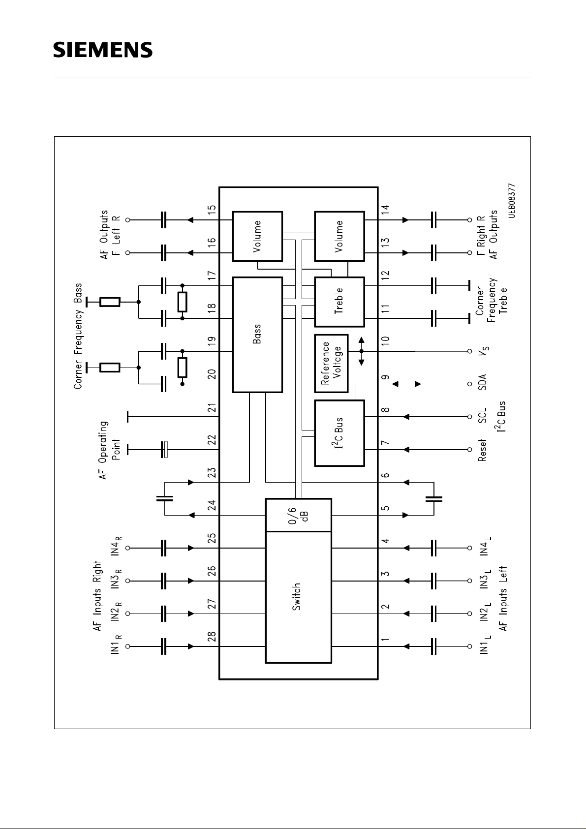
1.4 Functional Block Diagram
TDA 4390-2X
Figure 10
Block Diagram
Semiconductor Group 8 02.96
Page 9

TDA 4390-2X
2 Circuit Description
2.1 Signal Processing
1. The selection of the AF inputs happens in the input switch. There are four stereo
inputs available. An input level switch circuitry behind the input switch realizes the
adaption of different signal source levels. A gain of 0 dB or 6 dB is possible. After this
section a stereo output/input is placed for connecting external circuits like an
equalizer.
2. In the following signalpath there is tone control, consisting of bass and treble control.
Bass control offers a control range of + 18 dB to – 12 dB with a stepwidth of 2 dB.
Frequency characteristic, 1st order or 2nd order (resonance type) is fixed by external
components. Treble control offers a control range of ± 12 dB with a stepwidth of 2 dB.
The treble control corner frequency is fixed by an external capacitor. Last stage in
signalpath is volume control which can be adjusted independent for left, right, rear and
front. 57 steps with an increment of 1.25 dB give a setting range of 70 dB, the 57th
step activates muting.
2.2 Controlpart
All functions are controlled via an I
2
C Bus interface. All data is stored into a latch circuit.
The telegram structure is built as follows:
Startcondition – chipaddress – any number of databytes – stopcondition.
For the databytes the following conditions must be fulfilled:
first
Before transmitting a databyte a subaddress byte must
be placed in the data
telegram.
Semiconductor Group 9 02.96
Page 10
TDA 4390-2X
2.2.1 Chipaddress
MSB LSB
10000010
2.2.2 Subaddress bytes
MSB LSB
Volume front left ЧЧЧЧЧ000
Volume front right ЧЧЧЧЧ001
Volume rear left ЧЧЧЧЧ010
Volume rear right ЧЧЧЧЧ011
Bass/treble ЧЧЧЧЧ101
Switchbyte ЧЧЧЧЧ111
2.2.3 Controlbytes
a) Volume left, right, front, rear
MSB LSB
Max. volume ××111111
Max-1 ××111110
Max-16 ××110000
Max-55 ××001000
MUTE ××000111
MUTE ××000000
MUTE ××000×××
Power ON 0 0 0 0 0001
Semiconductor Group 10 02.96
Page 11
TDA 4390-2X
b) Treble/Bass
MSB LSB
Linear 1 0 001001
Max. treble, lin. bass 0 0 101001
Max. treble, lin. bass 0 0 0 × 1001
Min. treble, lin. bass 1 1 101001
Min. treble, lin. bass 1 1 1 × 1001
Lin. treble, max. bass 1 0 000000
Lin. treble, min. bass 1 0 001111
Max. treble, max. bass 0 0 0 × 0000
Min. treble, min. bass 1 1 1 × 1111
Power ON 0 0 000001
MSB
treble
LSB
treble
MSB
bass
LSB
bass
Semiconductor Group 11 02.96
Page 12

c) Switchbyte
TDA 4390-2X
MSB LSB
MUTE IN1 IN2 IN3 IN4 Gain ××
MUTE = 0
MUTE = 1
IN1 = 0
IN1 = 1
IN2 = 0
IN2 = 1
IN3 = 0
IN3 = 1
IN4 = 0
IN4 = 1
Gain = 0
Gain = 1
MUTE OFF; power ON
MUTE ON
Input1 OFF; power ON
Input1 ON
Input1 OFF; power ON
Input1 ON
Input1 OFF; power ON
Input1 ON
Input1 OFF; power ON
Input1 ON
Gain 0 dB; power ON
Gain 6 dB
If no signal is activated, this is interpreted as muting.
There is no mutual lockout of the inputs for multiple selections.
Semiconductor Group 12 02.96
Page 13

TDA 4390-2X
3 Electrical Characteristics
3.1 Absolute Maximum Ratings
T
= – 40 °C to 85 °C
A
Parameter Symbol Limit Values Unit Remarks
min. max.
Supply voltage
Max. DC voltage
Max. DC voltage
Max. DC voltage
Max. DC voltage
Max. DC voltage
Max. DC voltage
Max. DC voltage
Max. DC voltage
Max. DC voltage
Max. DC voltage
Max. DC voltage
Max. DC voltage
Max. DC voltage
Max. DC voltage
V
V
V
V
V
V
V
V
V
V
V
V
V
V
V
10
1
2
3
4
6
7
8
11
12
18
20
22
23
25
014V
0 V
0 V
0 V
0 V
0 V
0 V
10
10
10
10
10
10
V
V
V
V
V
V
06V
0 V
0 V
0 V
0 V
0 V
0 V
0 V
10
10
10
10
10
10
10
V
V
V
V
V
V
V
Max. DC voltage
Max. DC voltage
Max. DC voltage
Max. DC current
Max. DC current
Max. DC current
Max. DC current
Semiconductor Group 13 02.96
V
V
V
I
I
I
I
5
9
13
14
26
27
28
0 V
0 V
0 V
10
10
10
V
V
V
02mA
02mA
02mA
02mA
Page 14

TDA 4390-2X
3.1 Absolute Maximum Ratings (cont’d)
T
= – 40 °C to 85 °C
A
Parameter Symbol Limit Values Unit Remarks
min. max.
Max. DC current I
Max. DC current
Max. DC current
Max. DC current
Max. DC current
Junction temperature
Storage temperature
Thermal resistance
I
I
I
I
T
T
R
15
16
17
19
24
j
S
thSA
02mA
02mA
02mA
02mA
02mA
150 °C
– 40 125 °C
76 K/W
Note: Maximum ratings are absolute ratings; exceeding only one of these values may
cause irreversible damage to the integrated circuit.
3.2 Operating Range
Parameter Symbol Limit Values Unit
min. max.
Supply voltage
V
S
7.5 13.2 V
Ambient temperature range
Input frequency range ƒ
T
A
I
–40 85 °C
0.01 20 kHz
Note: In the operating range the functions given in the circuit description are fulfilled.
Semiconductor Group 14 02.96
Page 15

TDA 4390-2X
3.3 AC/DC Characteristics
V
= 10 V, TA = – 40 °C to 85 °C
S
Parameter Symbol Limit Values Unit Test Condition Test
min. typ. max.
Circuit
AF reference level 0 dB = 150 mV,
f
= 1 kHz, if not stated otherwise.
i
I2C Bus preset: Start – 82 – 00, 3F – 01, 3F – 02, 3F – 03, 3F – 05, 89 – 07, 40 – Stop
Chipaddr. – Vol 63 – Vol 63 – Vol 63 – Vol 63 – tone lin – IN1
The basic setting for each point in the specification is always preset; only settings which are deviate
from this, are given in the test conditions. Details in
italics
only provide explanation of the
hexadecimal code and which switch bits on the setbytes are stated.
Current
I
10
39 55 mA 1
consumption
A. Signal Section
1)
Gain
1)
Gain
1)
Gain
1)
Gain
Max. gain
Max. gain
Max. gain
Max. gain
Min. gain
Min. gain
Min. gain
Min. gain
Tracking error ∆
V
V
V
V
V
V
V
V
V
V
V
V
5-1
24-28
5-1
24-28
15-6
16-6
13-23
14-23
15-6
16-6
13-23
14-23
V
13-14
–101dB 1
–101dB 1
567dB07, 44;
567dB07, 44;
gain = 6 dB
gain = 6 dB
1
1
–202dB 1
–202dB 1
–202dB 1
–202dB 1
– 70 – 60 dB 00, 08-02, 08;
– 70 – 60 dB 00, 08-02, 08;
– 70 – 60 dB 01, 08-03, 08;
– 70 – 60 dB 01, 08-03, 08;
± 3 dB 01, 3F to 01, 24
03, 3F to 03, 24;
Vol 8
Vol 8
Vol 8
Vol 8
Vol 63-36
1
1
1
1
1
Tracking error ∆
Tracking error ∆
Tracking error ∆
1)
Same values apply for feeding in on pins 2 … 4, and 25 … 27.
V
V
V
15-16
13-16
14-15
± 3 dB 00, 3F to 00, 24
02, 3F to 02, 24;
± 3 dB 00, 3F to 00, 24
01, 3F to 01, 24;
± 3 dB 02, 3F to 02, 24
03, 3F to 03, 24;
1
Vol 63-36
1
Vol 63-36
1
Vol 63-36
Semiconductor Group 15 02.96
Page 16

TDA 4390-2X
3.3 AC/DC Characteristics (cont’d)
V
= 10 V, TA = – 40 °C to 85 °C
S
Parameter Symbol Limit Values Unit Test Condition Test
min. typ. max.
Circuit
Step width Vol
Step width Vol
Step width Vol
Step width Vol
Bass boost
Bass boost
Bass boost
Bass boost
Bass boost
13
∆V
13
0 1.25 2.5 dB 01, X-01, (X ± 1)
1
Vol X-Vol (X±1)
14
∆V
14
0 1.25 2.5 dB 03, X-03, (X ± 1)
1
Vol X-Vol (X± 1)
15
∆V
15
0 1.25 2.5 dB 02, X-02, (X ± 1)
1
Vol X-Vol (X± 1)
16
∆V
16
0 1.25 2.5 dB 02, X-02, (X ± 1)
1
Vol X-Vol (X± 1)
V
15-6
15 18 dB 05, 80; fi = 40 Hz
1
bass max, treble lin
V
16-6
15 18 dB 05, 80; fi = 40 Hz
1
bass max, treble lin
V
13-23
15 18 dB 05, 80; fi = 40 Hz
1
bass max, treble lin
V
14-23
15 18 dB 05, 80; fi = 40 Hz
1
bass max, treble lin
V
15-6
– 12 dB 05, 8F; fi = 40 Hz
1
bass min, treble lin
Bass boost
Bass boost
Bass boost
Step width bass ∆
Step width bass ∆
Step width bass ∆
Step width bass ∆
V
V
V
16-6
13-23
14-23
V
13
V
14
V
15
V
16
– 12 dB 05, 8F; fi = 40 Hz
bass min, treble lin
– 12 dB 05, 8F; fi = 40 Hz
bass min, treble lin
– 12 dB 05, 8F; fi = 40 Hz
bass min, treble lin
123dB05, 8X-05,8 (X ± 1)
bass X-bass (X±1)
123dB05, 8X-05,8 (X ± 1)
bass X-bass (X±1)
123dB05, 8X-05,8 (X ± 1)
bass X-bass (X±1)
123dB05, 8X-05,8 (X ± 1)
bass X-bass (X±1)
1
1
1
1
1
1
1
Semiconductor Group 16 02.96
Page 17

TDA 4390-2X
3.3 AC/DC Characteristics (cont’d)
V
= 10 V, TA = – 40 °C to 85 °C
S
Parameter Symbol Limit Values Unit Test Condition Test
min. typ. max.
Circuit
Treble boost V
Treble boost
Treble boost
Treble boost
Treble boost
Treble boost
Treble boost
Treble boost
Treble boost
V
V
V
V
V
V
V
V
15-6
16-6
13-23
14-23
15-6
15-6
16-6
13-23
14-23
9 12 dB 05, 09; fi = 15 kHz
treble max, bass lin
9 12 dB 05, 09; fi= 15 kHz
treble max, bass lin
9 12 dB 05, 09; fi = 15 kHz
treble max, bass lin
9 12 dB 05, 09; fi = 15 kHz
treble max, bass lin
9 12 dB 05, F9; fi = 15 kHz
treble min, bass lin
– 12 dB 05, F9; fi = 15 kHz
treble min, bass lin
– 12 dB 05, F9; fi = 15 kHz
treble min, bass lin
– 12 dB 05, F9; fi = 15 kHz
treble min, bass lin
– 12 dB 05, F9; fi = 15 kHz
treble min, bass lin
1
1
1
1
1
1
1
1
1
Step width treble ∆
Step width treble ∆
Step width treble ∆
Step width treble ∆
V
13
123dB05, X9-05, (X ± 1) 9
1
treble X-treble (X±1)
V
14
123dB05, X9-05, (X ± 1) 9
1
treble X-treble (X±1)
V
15
123dB05, X9-05, (X ± 1) 9
1
treble X-treble (X±1)
V
16
123dB05, X9-05, (X ± 1) 9
1
treble X-treble (X±1)
Semiconductor Group 17 02.96
Page 18

TDA 4390-2X
3.3 AC/DC Characteristics (cont’d)
V
= 10 V, TA = – 40 °C to 85 °C
S
Parameter Symbol Limit Values Unit Test Condition Test
min. typ. max.
Circuit
Tone linearity ∆V
13
± 3 dB 05, 89; fi = 40 Hz … 15 kHz
treble, bass lin
Tone linearity ∆
V
14
± 3 dB 05, 89; fi = 40 Hz … 15 kHz
treble, bass lin
Tone linearity ∆
V
15
± 3 dB 05, 89; fi = 40 Hz … 15 kHz
treble, bass lin
Tone linearity ∆
V
16
± 3 dB 05, 89; fi = 40 Hz … 15 kHz
treble, bass lin
Channel separation ∆
Channel separation ∆
Crosstalk of the
switch
Attenuation MUTE
Attenuation MUTE
1)
2)
2)
V
14-15
V
13-16
a
input unwanted/
output wanted
a
1-5
a
1-5
60 dB V6 or V23 = 300 mVrms 1
60 dB V6 or V23 = 300 mVrms 1
80 dB V
V
i wanted
i unwanted
= 0
= 300 mVrms
80 dB 01, 00-03, 00;
V
= 300 mVrms
1
80 dB 07, C0; V1 = 300 mVrms
MUTE active
Attenuation MUTE
a
1-5
80 dB 07, 00; V1 = 300 mVrms
2)
not select
Attenuation MUTE
Attenuation MUTE
3)
a
28-24
3)
a
28-24
80 dB 00, 00 to 03, 00;
V
= 300 mVrms;
28
80 dB 07, 00; V28 = 300 mVrms
MUTE active
Attenuation MUTE
3)
a
28-24
80 dB 07, 00; V28 = 300 mVrms
not select
1)
Same values apply for feeding in on pins 1 … 4 or 25 … 28, and measurement on pins 5 or 24.
2)
Analogous values apply for feeding in on pins 2, 3, 4.
3)
Same values apply for feeding in on pins 25, 26, 27.
1
1
1
1
1
1
; Vol 0
1
1
1
Vol 0
1
1
Semiconductor Group 18 02.96
Page 19

TDA 4390-2X
3.3 AC/DC Characteristics (cont’d)
V
= 10 V, TA = – 40 °C to 85 °C
S
Parameter Symbol Limit Values Unit Test Condition Test
Circuit
1
1
1
1
1
Max. input voltage
Max. input voltage
Max. input voltage
Max. input voltage
Max. input voltage
min. typ. max.
1)
V
1
1)
V
1
2)
V
28
2)
V
28
V
6
1.5 Vrms k
0.75 Vrms k
1.5 Vrms k
0.75 Vrms k
250 Vrms k
≤ 1%;
15, 16
R
= 2.2 kΩ
L15, 16
≤ 1 %; 07, 44
15, 16
R
= 2.2 kΩ
L15, 16
≤ 1%;
13, 14
R
= 2.2 kΩ
L13, 14
≤ 1 %; 07, 44
13, 14
R
= 2.2 kΩ
L13, 14
< 1 %; 05, XX
15, 16
any sound
Max. input voltage
Max. output voltage
Max. output voltage
Max. output voltage
Max. output voltage
Distortion
Distortion
Distortion
Distortion
Distortion
Distortion
Distortion
Distortion
Distortion
Distortion
1)
Same values apply for feeding in on pins 2, 3, 4.
2)
Same values apply for feeding in on pins 25, 26, 27.
3)
Same values apply for feeding in on pins 2 … 4 or 25 … 27.
3)
3)
3)
3)
3)
3)
3)
3)
3)
3)
V
23
V
13
V
14
V
15
V
16
k
5
k
24
k
13
k
14
k
15
k
16
k
13
k
14
k
15
k
16
250 Vrms k
2.0 Vrms k13 < 1 % 1
2.0 Vrms k14 < 1 % 1
2.0 Vrms k15 < 1 % 1
2.0 Vrms kv < 1 % 1
0.01 0.1 % V1 = 150 mVrms 1
0.01 0.1 % V28 = 150 mVrms 1
0.01 0.1 % V28 = 150 mVrms 1
0.01 0.1 % V28 = 150 mVrms 1
0.01 0.1 % V1 = 150 mVrms 1
0.01 0.1 % V1 = 150 mVrms 1
0.01 0.1 % V28 = 150 mVrms
0.01 0.1 % V28 = 150 mVrms
0.01 0.1 % V1 = 150 mVrms
0.01 0.1 % V1 = 150 mVrms
< 1 %; 05, XX
13, 14
any sound
01, 2F;
03, 2F;
02, 2F;
00, 2F;
Vol 47
Vol 47
Vol 47
Vol 47
1
1
1
1
1
Semiconductor Group 19 02.96
Page 20

TDA 4390-2X
3.3 AC/DC Characteristics (cont’d)
V
= 10 V, TA = – 40 °C to 85 °C
S
Parameter Symbol Limit Values Unit Test Condition Test
min. typ. max.
Distortion
Distortion
Distortion
Distortion
Signal/noise ratio
Signal/noise ratio
Signal/noise ratio
Signal/noise ratio
Signal/noise ratio
Signal/noise ratio
Signal/noise ratio
Signal/noise ratio
1)
Same values apply for feeding in on pins 2 … 4 or 25 … 27.
1)
1)
1)
1)
k
13
k
14
k
15
k
16
1)
a
S/N13
1)
a
S/N14
1)
a
S/N15
1)
a
S/N16
1)
a
S/N13
1)
a
S/N14
1)
a
S/N15
1)
a
S/N16
80 95 dB V
80 95 dB V
80 95 dB V
80 95 dB V
60 80 dB V
60 80 dB V
60 80 dB V
60 80 dB V
0.05 0.5 % V28 = 150 mVrms
0.05 0.5 % V28 = 150 mVrms
0.05 0.5 % V1 = 150 mVrms
0.05 0.5 % V1 = 150 mVrms
05, XX;
05, XX;
05, XX;
05, XX;
Nrms 20 Hz-20 kHz
V
28
Nrms 20 Hz-20 kHz
V
28
Nrms 20 Hz-20 kHz
V
1
Nrms 20 Hz-20 kHz
V
1
Nrms 20 Hz-20 kHz
V
28
01, 27;
Nrms 20 Hz-20 kHz
V
28
03, 27;
Nrms 20 Hz-20 kHz
V
1
Nrms 20 Hz-20 kHz
V
1
00, 27;
any sound
any sound
any sound
any sound
= 0.3 Vrms
= 0.3 Vrms
= 0.3 Vrms
= 0.3 Vrms
= 0.3 Vrms
Vol 39
= 0.3 Vrms
Vol 39
= 0.3 Vrms; 02, 27
= 0.3 Vrms
Vol 39
Circuit
1
1
1
1
1
1
1
1
1
1
1
1
Semiconductor Group 20 02.96
Page 21

TDA 4390-2X
3.3 AC/DC Characteristics (cont’d)
V
= 10 V, TA = – 40 °C to 85 °C
S
Parameter Symbol Limit Values Unit Test Condition Test
min. typ. max.
Circuit
Noise voltage V
Noise voltage V
Noise voltage V
Noise voltage V
DC jump ∆ 1 bit ∆
DC jump ∆ 1 bit ∆
DC jump ∆ 1 bit ∆
DC jump ∆ 1 bit ∆
DC jump ∆ 1 bit ∆
N13
N14
N15
N16
V
V
V
V
V
210µVrms V
210µVrms V
210µVrms V
210µVrms V
13
± 10 mV 01, X-01, (X ± 1)
Nrms 20 Hz-20 kHz
01, 00-03, 00;
Nrms 20 Hz-20 kHz
00, 00-03, 00;
Nrms 20 Hz-20 kHz
00, 00-02, 00;
Nrms 20 Hz-20 kHz
01, 00-02, 00;
Vol 0
Vol 0
Vol 0
Vol 0
1
1
1
1
1
Vol X-Vol (X± 1)
14
± 10 mV 03, X-03, (X ± 1)
1
Vol X-Vol (X± 1)
15
± 10 mV 02, X-02, (X ± 1)
1
Vol X-Vol (X± 1)
16
± 10 mV 00, X-00, (X ± 1)
1
Vol X-Vol (X± 1)
13
± 10 mV 05, X-05, (X ± 1)
1
tone X-tone (X± 1)
DC jump ∆ 1 bit ∆
DC jump ∆ 1 bit ∆
DC jump ∆ 1 bit ∆
PSRR
PSRR
PSRR
PSRR
V
V
V
A
PSRR13
A
PSRR14
A
PSRR15
A
PSRR16
14
± 10 mV 05, X-05, (X ± 1)
1
tone X-tone (X± 1)
15
± 10 mV 05, X-05, (X ± 1)
1
tone X-tone (X± 1)
16
± 10 mV 05, X-05, (X ± 1)
1
tone X-tone (X± 1)
70 dB V
f
undesired
= 1 Vrms
undesired
= 100 Hz … 20 kHz
1
70 dB input termination with 220 Ω 1
70 dB measurement rms
1
according CCIR 651
70 dB 1
Semiconductor Group 21 02.96
Page 22

TDA 4390-2X
3.3 AC/DC Characteristics (cont’d)
V
= 10 V, TA = – 40 °C to 85 °C
S
Parameter Symbol Limit Values Unit Test Condition Test
min. typ. max.
Design Hints
Circuit
Input resistance
Input resistance
Input resistance
Input resistance
Input resistance
Input resistance
Input resistance
Input resistance
Input resistance
Input resistance
Output resistance
Output resistance
Output resistance
Output resistance
Output resistance
Output resistance
R
1
R
2
R
3
R
4
R
6
R
23
R
25
R
26
R
27
R
28
R
5
R
13
R
14
R
15
R
v
R
24
22 27 kΩ
22 27 kΩ
22 27 kΩ
22 27 kΩ
24 30 kΩ
24 30 kΩ
22 27 kΩ
22 27 kΩ
22 27 kΩ
22 27 kΩ
200 Ω
200 Ω
200 Ω
200 Ω
200 Ω
200 Ω
V
= 8.5 V
s
Max. input voltage
V
6
180 mVrms k
< 5 %; 05, XX
15, 16
1
any sound
Max. input voltage
V
23
180 mVrms k
< 5 %; 05, XX
13, 14
1
any sound
Bass boost
V
15-6
10 12 dB 05,83; fi=40Hz
1
bass step 6, treble lin
Bass boost
V
16-6
10 12 dB 05,83; fi=40Hz
1
bass step 6, treble lin
Bass boost
V
13-23
10 12 dB 05,83; fi=40Hz
1
bass step 6, treble lin
Bass boost
V
14-23
10 12 dB 05,83; fi=40Hz
1
bass step 6, treble lin
Semiconductor Group 22 02.96
Page 23

TDA 4390-2X
3.3 AC/DC Characteristics (cont’d)
V
= 10 V, TA = – 40 °C to 85 °C
S
Parameter Symbol Limit Values Unit Test Condition Test
Circuit
V
= 12 V
s
min. typ. max.
Max. input voltage
Max. input voltage
2
C Bus (SCL, SDA edges)
B. I
Rise time
Fall time
V
6
V
23
t
R
t
F
Shift Register Clock Pulse SCL
Frequency
H-pulse width
L-pulse width
f
SCL
t
HIGH
t
LOW
Start
Set-up time
Hold time
t
SUSTA
t
HDSTA
300 mVrms k
300 mVrms k
300 ns
300 ns
0 400 kHz
0.6 µs
1.3 µs
0.6 µs
0.6 µs
< 1 %; 05, XX
15, 16
any sound
< 1 %; 05, XX
13, 14
any sound
1
1
Stop
Set-up time
Bus free time
t
SUSTO
t
BUF
0.6 µs
1.3 µs
Data Transfer
Set-up time t
Hold time
SUDAT
t
HDDAT
100 µs
0 0.9 µs
Semiconductor Group 23 02.96
Page 24

TDA 4390-2X
3.3 AC/DC Characteristics (cont’d)
V
= 10 V, TA = – 40 °C to 85 °C
S
Parameter Symbol Limit Values Unit Test Condition Test
min. typ. max.
Inputs SCL, SDA
Circuit
Input voltage
Hysteresis
Spike suppression
Input current
V
QH
V
QL
V
HYS
t
SP
I
QH
V
QL
3 5.5 V
1.5 V
0.2 V
50 ns
50 µA
100 µA
Output SDA (open collector)
Output voltage V
Reset inactive
Reset active
QH
V
QL
V
L
V
H
5.4 V RL = 2.5 kΩ
0.4 V IQL = 3 mA
1.5 V
3 5.5 V
Note: The listed characteristics are ensured over the operating range of the integrated
circuit. Typical characteristics specify mean values expected over the production
spread. If not otherwise specified, typical characteristics apply at
T
=25°C and
A
the given supply voltage.
Semiconductor Group 24 02.96
Page 25

TDA 4390-2X
3.4 AC/DC Characteristics
V
= 10 V, TA = 25 °C
S
Parameter Symbol Limit Values Unit Test Condition Test
min. typ. max.
Circuit
AF reference level 0 dB = 150 mV,
f
= 1 kHz, if not stated otherwise.
i
I2C Bus preset: Start – 82 – 00, 3F – 01, 3F – 02, 3F – 03, 3F – 05, 89 – 07, 40 – Stop
Chipaddr. – Vol 63 – Vol 63 – Vol 63 – Vol 63 – tone lin – IN1
The basic setting for each point in the specification is always preset; only settings which are deviate
from this, are given in the test conditions. Details in
italics
only provide explanation of the
hexadecimal code and which switch bits on the setbytes are stated.
Current
I
10
39 50 mA 1
consumption
A. Signal Section
1)
Gain
1)
Gain
1)
Gain
1)
Gain
Max. gain
Max. gain
Max. gain
Max. gain
Min. gain
Min. gain
Min. gain
Min. gain
Tracking error ∆
V
V
V
V
V
V
V
V
V
V
V
V
5-1
24-28
5-1
24-28
15-6
16-6
13-23
14-23
15-6
16-6
13-23
14-23
V
13-14
–101dB 1
–101dB 1
567dB07, 44;
567dB07, 44;
gain = 6 dB
gain = 6 dB
1
1
–202dB 1
–202dB 1
–202dB 1
–202dB 1
– 70 – 65 dB 00, 08-02, 0; 8
– 70 – 65 dB 00, 08-02, 0; 8
– 70 – 65 dB 01, 08-03, 0; 8
– 70 – 65 dB 01, 08-03, 08;
± 2 dB 01, 3F to 01, 24
03, 3F to 03, 24;
Vol 8
Vol 8
Vol 8
Vol 8
Vol 63-36
1
1
1
1
1
Tracking error ∆
Tracking error ∆
Tracking error ∆
1)
Same values apply for feeding in on pins 2 … 4, and 25 … 27.
V
V
V
15-16
13-16
14-15
± 2 dB 00, 3F to 00, 24
02, 3F to 02, 24;
± 2 dB 00, 3F to 00, 24
01, 3F to 01, 24;
± 2 dB 02, 3F to 02, 24
03, 3F to 03, 24;
1
Vol 63-36
1
Vol 63-36
1
Vol 63-36
Semiconductor Group 25 02.96
Page 26

TDA 4390-2X
3.4 AC/DC Characteristics (cont’d)
V
= 10 V, TA = 25 °C
S
Parameter Symbol Limit Values Unit Test Condition Test
min. typ. max.
Circuit
Step width Vol
Step width Vol
Step width Vol
Step width Vol
Bass boost
Bass boost
Bass boost
Bass boost
Bass boost
13
∆V
13
0 1.25 2.5 dB 01, X-01, (X ± 1)
1
Vol X-Vol (X±1)
14
∆V
14
0 1.25 2.5 dB 03, X-03, (X ± 1)
1
Vol X-Vol (X± 1)
15
∆V
15
0 1.25 2.5 dB 02, X-02, (X ± 1)
1
Vol X-Vol (X± 1)
16
∆V
16
0 1.25 2.5 dB 00, X-00, (X ± 1)
1
Vol X-Vol (X± 1)
V
15-6
16 18 dB 05, 80; fi = 40 Hz
1
bass max, treble lin
V
16-6
16 18 dB 05, 80; fi = 40 Hz
1
bass max, treble lin
V
13-23
16 18 dB 05, 80; fi = 40 Hz
1
bass max, treble lin
V
14-23
16 18 dB 05, 80; fi = 40 Hz
1
bass max, treble lin
V
15-6
– 12 dB 05, 8F; fi = 40 Hz
1
bass min, treble lin
Bass boost
Bass boost
Bass boost
Step width bass ∆
Step width bass ∆
Step width bass ∆
Step width bass ∆
V
V
V
16-6
13-23
14-23
V
13
V
14
V
15
V
16
– 12 dB 05, 8F; fi = 40 Hz
bass min, treble lin
– 12 dB 05, 8F; fi = 40 Hz
bass min, treble lin
– 12 dB 05, 8F; fi = 40 Hz
bass min, treble lin
123dB05, 8X-05, 8 (X ± 1)
bass X-bass (X±1)
123dB05, 8X-05, 8 (X ± 1)
bass X-bass (X±1)
123dB05, 8X-05, 8 (X ± 1)
bass X-bass (X±1)
123dB05, 8X-05, 8 (X ± 1)
bass X-bass (X±1)
1
1
1
1
1
1
1
Semiconductor Group 26 02.96
Page 27

TDA 4390-2X
3.4 AC/DC Characteristics (cont’d)
V
= 10 V, TA = 25 °C
S
Parameter Symbol Limit Values Unit Test Condition Test
min. typ. max.
Circuit
Treble boost V
Treble boost
Treble boost
Treble boost
Treble boost
Treble boost
Treble boost
Treble boost
Treble boost
V
V
V
V
V
V
V
V
15-6
16-6
13-23
14-23
15-6
15-6
16-6
13-23
14-23
10 12 dB 05, 09; fi = 15 kHz
treble max, bass lin
10 12 dB 05, 09; fi = 15 kHz
treble max, bass lin
10 12 dB 05, 09; fi = 15 kHz
treble max, bass lin
10 12 dB 05, 09; fi = 15 kHz
treble max, bass lin
10 12 dB 05, F9; fi = 15 kHz
treble min, bass lin
– 12 dB 05, F9; fi = 15 kHz
treble min, bass lin
– 12 dB 05, F9; fi = 15 kHz
treble min, bass lin
– 12 dB 05, F9; fi = 15 kHz
treble min, bass lin
– 12 dB 05, F9; fi = 15 kHz
treble min, bass lin
1
1
1
1
1
1
1
1
1
Step width treble ∆
Step width treble ∆
Step width treble ∆
Step width treble ∆
V
13
123dB05, X9-05, (X ± 1) 9
1
treble X-treble (X±1)
V
14
123dB05, X9-05, (X ± 1) 9
1
treble X-treble (X±1)
V
15
123dB05, X9-05, (X ± 1) 9
1
treble X-treble (X±1)
V
16
123dB05, X9-05, (X ± 1) 9
1
treble X-treble (X±1)
Semiconductor Group 27 02.96
Page 28

TDA 4390-2X
3.4 AC/DC Characteristics (cont’d)
V
= 10 V, TA = 25 °C
S
Parameter Symbol Limit Values Unit Test Condition Test
min. typ. max.
Circuit
Tone linearity ∆V
13
± 2 dB 05, 89; fi = 40 Hz … 15 kHz
treble, bass lin
Tone linearity ∆
V
14
± 2 dB 05, 89; fi = 40 Hz … 15 kHz
treble, bass lin
Tone linearity ∆
V
15
± 2 dB 05, 89; fi = 40 Hz … 15 kHz
treble, bass lin
Tone linearity ∆
V
16
± 2 dB 05, 89; fi = 40 Hz … 15 kHz
treble, bass lin
Channel separation ∆
Channel separation ∆
Crosstalk of the
switch
Attenuation MUTE
Attenuation MUTE
1)
2)
2)
V
14-15
V
13-16
a
input unwanted/
output wanted
a
1-5
a
1-5
60 dB V6 or V23 = 300 mVrms 1
60 dB V6 or V23 = 300 mVrms 1
80 dB V
V
i wanted
i unwanted
= 0
= 300 mVrms
80 dB 01, 00-03, 00;
V
= 300 mVrms;
1
80 dB 07, C0; V1 = 300 mVrms
MUTE active
Attenuation MUTE
a
1-5
80 dB 07, 00; V1 = 300 mVrms
2)
not select
Attenuation MUTE
Attenuation MUTE
a
28-24
3)
a
28-24
80 dB 00, 00 to 03, 00;
V
= 300 mVrms;
28
80 dB 07, C0; V28 = 300 mVrms
3)
MUTE active
Attenuation MUTE
a
28-24
80 dB 07, 00; V28 = 300 mVrms
3)
not select
1)
Same values apply for feeding in on pins 1 … 4 or 25 … 28, and measurement on pins 5 or 24.
2)
Analogous values apply for feeding in on pins 2, 3, 4.
3)
Same values apply for feeding in on pins 25, 26, 27.
1
1
1
1
1
1
Vol 0
1
1
1
Vol 0
1
1
Semiconductor Group 28 02.96
Page 29

TDA 4390-2X
3.4 AC/DC Characteristics (cont’d)
V
= 10 V, TA = 25 °C
S
Parameter Symbol Limit Values Unit Test Condition Test
Circuit
1
1
1
1
1
Max. input voltage
Max. input voltage
Max. input voltage
Max. input voltage
Max. input voltage
min. typ. max.
1)
V
1
1)
V
1
2)
V
28
2)
V
28
V
6
2 Vrms k
1 Vrms k
2 Vrms k
1 Vrms k
280 Vrms k
≤ 1%;
15, 16
R
= 2.2 kΩ
L15, 16
≤ 1 %; 07, 44
15, 16
R
= 2.2 kΩ
L15, 16
≤ 1%;
13, 14
R
= 2.2 kΩ
L13, 14
≤ 1 %; 07, 44
13, 14
R
= 2.2 kΩ
L13, 14
< 1 %; 05, XX
15, 16
any sound
Max. input voltage
Max. output voltage
Max. output voltage
Max. output voltage
Max. output voltage
Distortion
Distortion
Distortion
Distortion
Distortion
Distortion
Distortion
Distortion
Distortion
Distortion
1)
Same values apply for feeding in on pins 2, 3, 4.
2)
Same values apply for feeding in on pins 25, 26, 27.
3)
Same values apply for feeding in on pins 2 … 4 or 25 … 27.
3)
3)
3)
3)
3)
3)
3)
3)
3)
3)
V
23
V
13
V
14
V
15
V
16
k
5
k
24
k
13
k
14
k
15
k
16
k
13
k
14
k
15
k
16
280 Vrms k
2.2 Vrms k13 < 1 % 1
2.2 Vrms k14 < 1 % 1
2.2 Vrms k15 < 1 % 1
2.2 Vrms k16 < 1 % 1
0.01 0.05 % V1 = 150 mVrms 1
0.01 0.05 % V28 = 150 mVrms 1
0.01 0.05 % V28 = 150 mVrms 1
0.01 0.05 % V28 = 150 mVrms 1
0.01 0.05 % V1 = 150 mVrms 1
0.01 0.05 % V1 = 150 mVrms 1
0.01 0.1 % V28 = 150 mVrms
0.01 0.1 % V28 = 150 mVrms
0.01 0.1 % V1 = 150 mVrms
0.01 0.1 % V1 = 150 mVrms
< 1 %; 05, XX
13, 14
any sound
01, 2F;
03, 2F;
02, 2F;
00, 2F;
Vol 47
Vol 47
Vol 47
Vol 47
1
1
1
1
1
Semiconductor Group 29 02.96
Page 30

TDA 4390-2X
3.4 AC/DC Characteristics (cont’d)
V
= 10 V, TA = 25 °C
S
Parameter Symbol Limit Values Unit Test Condition Test
min. typ. max.
Distortion
Distortion
Distortion
Distortion
Signal/noise ratio
Signal/noise ratio
Signal/noise ratio
Signal/noise ratio
Signal/noise ratio
Signal/noise ratio
Signal/noise ratio
Signal/noise ratio
1)
Same values apply for feeding in on pins 2 … 4 or 25 … 27.
1)
1)
1)
1)
k
13
k
14
k
15
k
16
1)
a
S/N13
1)
a
S/N14
1)
a
S/N15
1)
a
S/N16
1)
a
S/N13
1)
a
S/N14
1)
a
S/N15
1)
a
S/N16
90 95 dB V
90 95 dB V
90 95 dB V
90 95 dB V
70 80 dB V
70 80 dB V
70 80 dB V
70 80 dB V
0.05 0.2 % V28 = 150 mVrms
0.05 0.2 % V28 = 150 mVrms
0.05 0.2 % V1 = 150 mVrms
0.05 0.2 % V1 = 150 mVrms
05, XX;
05, XX;
05, XX;
05, XX;
Nrms 20 Hz-20 kHz
V
28
Nrms 20 Hz-20 kHz
V
28
Nrms 20 Hz-20 kHz
any sound
any sound
any sound
any sound
= 0.3 Vrms
= 0.3 Vrms
V1 = 0.3 Vrms
Nrms 20 Hz-20 kHz
V1 = 0.3 Vrms
Nrms 20 Hz-20 kHz
V
= 0.3 Vrms
28
01, 27;
Nrms 20 Hz-20 kH
V
28
03, 27;
Nrms 20 Hz-20 kHz
V
1
Nrms 20 Hz-20 kHz
V
1
00, 27;
Vol 39
z
= 0.3 Vrms
Vol 39
= 0.3 Vrms; 02, 27
= 0.3 Vrms
Vol 39
Circuit
1
1
1
1
1
1
1
1
1
1
1
1
Semiconductor Group 30 02.96
Page 31

TDA 4390-2X
3.4 AC/DC Characteristics (cont’d)
V
= 10 V, TA = 25 °C
S
Parameter Symbol Limit Values Unit Test Condition Test
min. typ. max.
Circuit
Noise voltage V
Noise voltage
Noise voltage
Noise voltage
DC jump ∆ 1 bit ∆
DC jump ∆ 1 bit ∆
DC jump ∆ 1 bit ∆
DC jump ∆ 1 bit ∆
DC jump ∆ 1 bit ∆
N13
V
N14
V
N15
V
N16
V
13
25µVrms V
25µVrms V
25µVrms V
25µVrms V
± 10 mV 01, X-01, (X ± 1)
Nrms 20 Hz-20 kHz
01, 00-03, 00;
Nrms 20 Hz-20 kHz
01, 00-03, 00;
Nrms 20 Hz-20 kHz
00, 00-02, 00;
Nrms 20 Hz-20 kHz
00, 00-02, 00;
Vol 0
Vol 0
Vol 0
Vol 0
1
1
1
1
1
Vol X-Vol (X± 1)
V
4
1
± 10 mV 03, X-03, (X ± 1)
1
Vol X-Vol (X± 1)
V
15
± 10 mV 02, X-02, (X ± 1)
1
Vol X-Vol (X± 1)
V
16
± 10 mV 00, X-00, (X ± 1)
1
Vol X-Vol (X± 1)
V
13
± 10 mV 05, X-05, (X ± 1)
1
tone X-tone (X± 1)
DC jump ∆ 1 bit ∆
DC jump ∆ 1 bit ∆
DC jump ∆ 1 bit ∆
PSRR
PSRR
PSRR
PSRR
V
V
V
A
PSRR13
A
PSRR14
A
PSRR15
A
PSRR16
14
± 10 mV 05, X-05, (X ± 1)
1
tone X-tone (X± 1)
15
± 10 mV 05, X-05, (X ± 1)
1
tone X-tone (X± 1)
16
± 10 mV 05, X-05, (X ± 1)
1
tone X-tone (X± 1)
70 dB V
undesired
f
undesired
70 dB input termination
= 1 Vrms
= 100 Hz … 20 kHz
1
1
with 220 Ω
70 dB measurement rms
1
according CCIR 651
70 dB 1
Semiconductor Group 31 02.96
Page 32

TDA 4390-2X
3.4 AC/DC Characteristics (cont’d)
V
= 10 V, TA = 25 °C
S
Parameter Symbol Limit Values Unit Test Condition Test
min. typ. max.
Design Hints
Circuit
Input resistance
Input resistance
Input resistance
Input resistance
Input resistance
Input resistance
Input resistance
Input resistance
Input resistance
Input resistance
Output resistance
Output resistance
Output resistance
Output resistance
Output resistance
Output resistance
R
1
R
2
R
3
R
4
R
6
R
23
R
25
R
26
R
27
R
28
R
5
R
13
R
14
R
15
R
16
R
24
23 27 kΩ
23 27 kΩ
23 27 kΩ
23 27 kΩ
25.5 30 kΩ
25.5 30 kΩ
23 27 kΩ
23 27 kΩ
23 27 kΩ
23 27 kΩ
200 Ω
200 Ω
200 Ω
200 Ω
200 Ω
200 Ω
V
= 8.5 V
s
Max. input voltage
V
6
220 mVrms k
< 5 %; 05, XX
15, 16
1
any sound
Max. input voltage
V
23
220 mVrms k
< 5 %; 05, XX
13, 14
1
any sound
Bass boost
V
15-6
11 12 dB 05,83; fi=40Hz
1
bass step 6, treble lin
Bass boost
V
16-6
11 12 dB 05,83; fi=40Hz
1
bass step 6, treble lin
Bass boost
V
13-23
11 12 dB 05,83; fi=40Hz
1
bass step 6, treble lin
Bass boost
V
14-23
11 12 dB 05,83; fi=40Hz
1
bass step 6, treble lin
Semiconductor Group 32 02.96
Page 33

TDA 4390-2X
3.4 AC/DC Characteristics (cont’d)
V
= 10 V, TA = 25 °C
S
Parameter Symbol Limit Values Unit Test Condition Test
Circuit
V
= 12 V
s
min. typ. max.
Max. input voltage
Max. input voltage
2
C Bus (SCL, SDA edges)
B. I
Rise time
Fall time
V
6
V
23
t
R
t
F
Shift Register Clock Pulse SCL
Frequency f
H-pulse width
L-pulse width
SCL
t
HIGH
t
LOW
Start
Set-up time
Hold time
t
SUSTA
t
HDSTA
370 mVrms k
370 mVrms k
300 ns
300 ns
0 400 kHz
0.6 µs
1.3 µs
0.6 µs
0.6 µs
< 1 %; 05, XX
15, 16
any sound
< 1 %; 05, XX
13, 14
any sound
1
1
Stop
Set-up time
Bus free time
t
SUSTO
t
BUF
0.6 µs
1.3 µs
Data Transfer
Set-up time
Hold time
t
SUDAT
t
HDDAT
100 µs
0 0.9 µs
Semiconductor Group 33 02.96
Page 34

TDA 4390-2X
3.4 AC/DC Characteristics (cont’d)
V
= 10 V, TA = 25 °C
S
Parameter Symbol Limit Values Unit Test Condition Test
min. typ. max.
Inputs SCL, SDA
Circuit
Input voltage
Hysteresis
Spike suppression
Input current
V
QH
V
QL
V
HYS
t
SP
I
QH
V
QL
3 5.5 V
1.5 V
0.2 V
50 ns
50 µA
100 µA
Output SDA (open collector)
Output voltage
Reset inactive
Reset active
V
QH
V
QL
V
L
V
H
5.4 V RL = 2.5 kΩ
0.4 V IQL = 3 mA
1.5 V
3 5.5 V
Note: The listed characteristics are ensured over the operating range of the integrated
circuit. Typical characteristics specify mean values expected over the production
spread. If not otherwise specified, typical characteristics apply at
T
=25°C and
A
the given supply voltage.
Semiconductor Group 34 02.96
Page 35

TDA 4390-2X
Figure 11
Test Circuit
Semiconductor Group 35 02.96
Page 36

TDA 4390-2X
Figure 12
Application Circuit
Semiconductor Group 36 02.96
Page 37

TDA 4390-2X
Figure 13
Application Circuit
Semiconductor Group 37 02.96
Page 38

TDA 4390-2X
Figure 14
2
I
C Bus Timing
Semiconductor Group 38 02.96
Page 39

4 Package Outlines
P-DSO-28-3
(Plastic Dual Small Outline Package)
TDA 4390-2X
Sorts of Packing
Package outlines for tubes, trays etc. are contained in our
Data Book “Package Information”.
SMD = Surface Mounted Device
GPS05182
Dimensions in mm
Semiconductor Group 39 02.96
 Loading...